TECHNICAL PAPERS
SOLID-STATE SCIENCE AND TECHNOLOGY
A New Tungsten Gate Metal Oxide Semiconductor Capacitor
Using a Chemical Vapor Deposition Process
Wen-Kuan Yeh, Yeu-Cherng Shiau, and Mao-Chieh Chen*
Department of Electronics Engineering, National Chiao Tung University and National Nano Device Laboratory, Hsinchu, Taiwan
ABSTRACT
A new process for tungsten gate metal oxide semiconductor (MOS) capacitors has been developed using chemical vapor deposition (CVD) of tungsten on a thin poly-Si layer of appropriate thickness. The poly-Si acts as a sacrificial layer and is consumed during the CVD of tungsten (W). This process yields a nearly pure W metal gate after SiH4 reduction of WF6 at 300°C. Compared with sputtered tungsten films, the CVD tungsten film has lower resistivity and lower intrinsic film stress. In addition, the CVD tungsten metal gate MOS capacitor has a lower interface state density (D18) and a
high-er charge-to-breakdown (Q84), than sputter-deposited tungsten gate MOS capacitors.
Infroduction
Asdevice dimensions continue to decrease for higher density and improved performance in integrated circuits, there is a growing demand for more highly conductive gate and interconnection materials. The poly-Si now used for this purpose in conventional processing has certain limita-tions, due mainly to limited conductivity. In addition, it is well known that the use of p-polygates has become indis-pensable for p-channel metal oxide semiconductor field
effect transistors (MOSFET5) in the deep submicron regime. However; the penetration of boron impurities results in a shift of the threshold voltage, an increase in
subthreshold swing and leakage current, and degradation of the gate oxide reliability.1-3 Metal silicides4' have been
considered because their conductivities are higher than
that of poly-Si by one order of magnitude. Furthermore, it is expected that materials with conductivities higher than
those of silicides will be required in the future for very
high density integrated circuits. Thngsten is considered a very promising gate material candidate because it makes
gate implantation unnecessary. Furthermore, tungsten
also provides low resistivity and near midgap work func-tion.7 Tungsten gates have conventionally been prepared by sputtering,8 plasma- or laser-enhanced chemical vapor
deposition (CVD).9"° However, conventional CVD of tung-sten using silane or hydrogen reduction of WF, cannot deposit W on oxides at temperatures below 400°C.
Al-though tungsten can be forced directly onto Si02 surfaces at temperatures above 400°C, the resulting films possess 3-type structures with high resistivity'2 and tend to peel off because of poor adhesion to the Si02. In this study, we developed a new process, in which CVD of tungsten was employed to deposit W on a thin sacrificial poly-Si layer deposited on a gate oxide prior to CVD of the W itself. The
natural self-limiting Si consumption property of the
chemical vapor deposition of tungsten,'3 the so-called Si reduction reaction, will cause the thin sacrificial poly-Si layer to be consumed, so that a nearly pure W metal-gate MOS capacitor will result at the low deposition tempera-ture of 300°C. We introduce the first tungsten metal gate
Electrochemical Society Active Member.
(the poly-Si layer is completely consumed) MOS capacitor with the tungsten-gate formed by CVD process; this differs
from conventional tungsten-polycide gates'4 and
tung-sten/poly-Si gate MOS capacitors.'5 Our MOS capacitors are superior to sputter-deposited W gate capacitors with respect to MOS device applications.
Experimental
Samples were fabricated on (100) oriented p-type Si wafers. After initial RCA cleaning, 10 nm gate oxides were thermally grown in dry oxygen ambient at 92 5°C, followed by deposition of poly-Si layers of different thicknesses.
Tungsten films of 200 nm thickness were then deposited
using a CVD process via silane reduction of WF,, under the
following conditions: substrate temperature 300°C, total
gas pressure 100 mTorr, WF6 flow rate 20 sccm, SiH4 flow rate 10 sccm, and 112carrier-gasflow rate 1000 sccm. For
comparison purposes, sputtered-W-gate capacitors and conventional n-poly-Si-gate capacitors were also fabri-cated. For the sputtered-W-gate capacitors, the W gate was deposited directly on the gate oxide using dc
mag-netron sputtering in Ar ambient at a pressure of 8 mTorr and a deposition rate of 3 nm/mm. For the conventional
n-poly-Si-gate capacitors, the poly-Si gate was 300 nm
thick and was doped with POC13 at 950°C for 35 mm. The completed W-gate and polygate capacitors were treated with 60 s rapid thermal annealing (ETA) in N2 ambient at
temperatures ranging from 600 to 1000°C. The poly-Si
consumption thickness of the tungsten CVD process was
measured using cross-sectional transmission electron
microscopy (TEM). The electrical characteristics of the MOS capacitors were evaluated by C-V and I-V measure-ments. Stress in the W film was measured using a Tencor FLX-2320 thin-film stress measurement device.
Resultsand Discussion
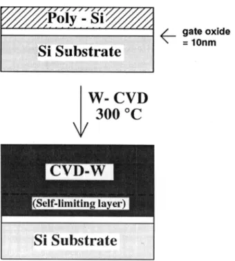
Figure1 shows the proposed process flow. The chemical vapor deposited tungsten film is easily deposited on the poly-Si surface at 3 00°C. Figure 2 shows cross-sectional TEM photographs of W gates with poly-Si layers of differ-ent thicknesses prior to CVD of tungsten: the polysilicon
layer thickness is 45 nm (a) and 25 nm (b). The poly-Si was 214 J. Electrochem. Soc., Vol. 144, No. 1, January 1997 The Electrochemical Society, Inc.
) unless CC License in place (see abstract).
ecsdl.org/site/terms_use
address. Redistribution subject to ECS terms of use (see
140.113.38.11
J. Electrochem. Soc., Vol. 144, No. 1, January 1997 The Electrochemical Society, Inc. 215
W-CVD
300 °C
gate oxide
\ =lOnm
Fig. 1. Proposed process flow for CVD-W-gate MOS capacitor
using a sacrificial poly-Si layer.
consumedat the initial stage by the tungsten CVD process
and the amount of consumption remained constant for
given a deposition condition irrespective of the deposited
W film thickness. In this study, the sacrificial poly-Si layer
was approximately 25 nm thick; thus, it nearly disap-peared from samples upon which 25 nm poly-Si was
deposited prior to the tungsten deposition.
Figure 3 shows the capacitance-voltage (C-V) character-istics of the CVD tungsten gate MOS capacitors with dif-ferent sacrificial poly-Si layer thicknesses. MOS capaci-tors with 45 nm thick sacrificial layer of poly-Si yielded a clear discrepancy between high frequency and quasi-static
C-V curves in accumulation mode, as shown in Fig. 3a; this
discrepancy is attributable to the high-resistivity undoped poly-Si layer remaining after CVD.MOScapacitors start-ed with 25 rim thick poly-Si sacrificial layers had a negli-gible discrepancy between their high frequency and quasi-static C-V curves in accumulation mode due to residual
poly-Si, as shown in Fig. 3b. Furthermore, any residual
poly-Si was later consumed by WSr formation during the subsequent thermal annealing.
Figure 4 shows the sheet resistance (R) vs. annealing
temperature for the W/poly-Si/Si02/Si samples with
dif-ferent initial poly-Si thicknesses. Samples with 45 or 30 nm thick initial poly-Si layers showed increased R,
after annealing at 600°C, presumbly due to transformation
of W into the WSi phase (1 <
x
< 2). The WSi phaseformed at temperatures up to 600°C has a hexagonal
struc-ture; however, this changes to a lower resistivity
tetra-gonal structure at temperatures above 600°C. 16Thus,the sheet resistance of the samples decreased after annealing at temperatures above 600°C. Since samples with 45 nm
thick initial poly-Si layers presumably consumed more tungsten during WSi, formation than those with 30 nm
thick initial poly-Si layers, the samples with 45 nm thick poly-Si layers showed higher R, values. Samples with ini-tial poly-Si layer 25 rim thick had no poly-Si remaining after CVD of tungsten and pure tungsten gate MOS struc-tures were obtained. Annealing of these samples therefore
Fig. 2. Cross-sectional TEM photo9raphs of CVD-W films
deposit-ed on (a) 45 nm Si/lO nm Si02/Si and (b) 25 nm
poly-Si/i 0 nm Si02/Si substrates.
W(200nm)/PoIy(25nm)/Ox(1 Onm)/Sl
I I I
0
Vg (Volts)
Fig. 3. Capacitance-voltage characteristics of the CVD-Wgate
MOS capacitors with initial poly-Si sacrificial layer of (a) 45 and (b) 25 nm thickness prior to CVD of W.
POIy
-Si
Substrate
c)
L) 0 L) L) 1.5 1 0.5 0 1.5 1 0.5 0 I—-\LIIE
-3 3) unless CC License in place (see abstract).
ecsdl.org/site/terms_use
address. Redistribution subject to ECS terms of use (see
140.113.38.11
216 J. Electrochem. Soc., Vol. 144, No. 1, January 1997 The Electrochemical Society, Inc.
200 300 400 500 600 700 800 9001000
Anneal
Temperature (°C)
Fig.4. Sheet resistance vs. annealing temperature for
W/(poly-Si) /5i02/Si samples with various initial poly-Si thicknesses.
involvedno W suicide formation, and the sheet resistance
correlation to the annealing temperature differed from
samples that had thicker initial poly-Si layers. The x-ray
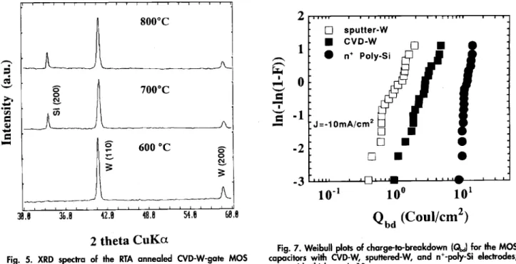
diffraction (XRD) spectra of these samples after RTA
annealing at 600, 700, and 800°C are shown in Fig. 5. The (110) and (200) W signals indicate that the samples were low resistivity a-W phase and remained unchanged even after annealing at the temperature of 800°C. No WSi, sig-nal was detected for these samples.
Dielectric strength of the W gate MOS capacitors was also investigated. Figure 6 shows the distribution of the dielectric breakdown fields for the CVD tungsten-gate and
the sputtered-tungsten-gate MOS capacitors, as well as
the n-poly-Si-gate capacitors. It can be seen that the
average breakdown field of the CVD-tungsten-gate MOS capacitors is comparable with those of the
sputtered-W-gate and n-po1y-Si sputtered-W-gate MOS capacitors. Charge-to-breakdown (Qbd) was measured using constant-current
stress on the 100 x100p.m capacitors at a current density
of 10 mA/cm2. Figure 7 shows the Weibull plots of
charge-.— 1,j —
1 0
'—. 8060
40
20 0(b)
I I IE sputter-W
gate No. of sample • =4opointsIIIn.
-__
Breakdown Field (MV/cm)
Fig. 6. Dielectric breakdown Field distribution for the MOS
capac-itors with CVD-W, sputtered-W, and n-poly-Si electrodes; gate
oxide thickness is 10 nm. l2 4 3
2
1 0..-•--- poly-Si
= 45nm
—Li
-poly-Si
= 3Onm• poly-Si =
25nm 100(a)
°—' 80S
60
40
20 lb1 0
CVD-W gate.ii,
'—' 80
60
I. 2010 11 12 13 14 15 16 17
2
U sputter-W
1U •
I
:,::0m:!:,,
101
100 101bd
(Coul/cm2)
Fig.7. Weibull plots of charge-to-breakdown (Q) for the MOS capacitors with CVD-W, sputtered-W, and n-poly-Si electrodes;
gate oxide thickness is 10 nm.
2 theta CuKa
Fig. 5. XRD spectra of the RTA annealed CVD-W-gate MOS
capacitors.
) unless CC License in place (see abstract).
ecsdl.org/site/terms_use
address. Redistribution subject to ECS terms of use (see
140.113.38.11
J. Electrochem. Soc., Vol. 144, No.1, January 1997 The Electrochemical Society, Inc. 217 to-breakdown (Qbd) for the CVD-tungsten-,
sputtered-tungsten-, and n-poly-Si-gate MOS capacitors. Although the Qbdofthe CVD-tungsten-gate capacitor is lower than that of the conventional n-poly-Si-gate capacitors, it is
much larger than that of the sputtered-tungsten gate
capacitors. This is presumably due to the large film stress of the sputtered-W-gate, which was found to be 1 X 10¹⁰
dyn/cm2.Large stress tends to induce a high interface state
charge density (Q10) and fixed-oxide charge density (Q1).'7
Thus, in order to maintain a constant current injection, the
gate voltage must be increased,which leads to earlier
breakdown of the oxide dielectric.
Figure 8 shows the flatband voltage (V0) plotted against annealing temperature for the CVD-tungsten-, sputtered-tungsten-, and n-poly-Si-gate MOS capacitors. The VFB of the CVD-tungsten-gate capacitor was —0.32 V (after post-metallization sintering at 400°C), and only a slight
change of 0.12 V in VE. occurred over a wide range of annealing temperatures up to 1000°C. The slight difference
in flatband voltage (VFB) between the CVD-tungsten-gate
and sputtered-tungsten-gate MOS capacitors was
pre-sumably due to the discrepancy of work function between the CVD and sputtered tungsten. Table I gives a compari-son of characteristics between the CVD-tungsten-gate and sputtered-tungsten-gate MOS capacitors. The
CVD-tung-sten films showed an ct-type structure, as revealed by x-ray diffraction analysis, and had a low resistivity of 12.5 pSI cm, compared with a resistivity of more than 46 1jfl
cm for the sputtered-tungsten films. The initial stress of the CVD-tungsten film was tensile, and lower than that of
the sputtered-tungsten film, which was compressively
stressed. The midgap interface state density (D11) of the CVD-tungsten-gate MOS capacitor was found to be about 1010 eV cm2, which was lower than that of the sputtered-tungsten-gate MOS by one order of magnitude. The large
film stress of the sputtered-tungsten-gate capacitor
ap-parently induced a large number of interface trap states.
Flatband voltage variations of the CVD-tungsten-gate
capacitors and the sputtered-tungsten-gate capacitors are comparable over a wide range of annealing temperatures
up to 1000°C.
Conclusion
Anew CVD-tungsten-gate MOS process has been pro-posed. After an appropriate thickness of sacrificial poly-Si
layer has been deposited on the gate oxide, W film can
eas-ily be deposited using the CVD process at low tempera-tures. The chemical vapor deposition of tungsten results in complete consumption of the sacrifical poly-Si layer,
lead-C
-0..
Anneal Temperature (°C)
Fig. 8. Flatband voltage vs. annealing temperature for the MOS capacitors with CVD-W, sputtered-W, and n-poly Si electrodes;
gate oxide thickness is 10 nm.
Table I. Characteristics of MOS capacitors with chemical-vapor deposited-W and sputtered-W electrodes; gate oxide
thickness is 10 nm.
CVD-W-gate
MOS Sputtered-W-gateMOS W film resistivity (pAl cm) Wfilm stress 12.5 5.4 x 10' 46.7 x 10¹⁰ (dyne/cm2) Ili, (eV cm2)' (tensile) )<
10
(compressive)2 >< 1011 z\V 0.12 0.09 (V) Gate oxide =10nm. D,,: interface state density.AV,,: flathand voltage variation after anneal at temperatures up to 1000°C.
ing to a nearly pure tungsten-gate MOS. Compared with
sputtered-tungsten-gate MOS capacitors, the proposed
MOS capacitor has a lower resistivity gate, lower intrinsic tungsten film stress, lower interface state density (D1j, and higher charge-to-breakdown (Qbd). These basic
character-istics indicate that the proposed MOS capacitors show
great promise for future VLSI application. Acknowledgments
This work was supported by National Science Council
(ROC) under Contract No. NSC84-2622-E009-007-1.
Manuscript submitted Nov. 1, 1995; revised manuscript
received Sept. 14, 1996.
National Chiao Tang University assisted in meeting the publcation costs of this article.
REFERENCE
1. G. J. Hu and R. H. Bruce, IEEE Trans. Electron
De-vices, ED-32, 584 (1985).
2. J. Y.-C. Sun, C. Wong, Y. Taur, and C.-H. Hsu, in Digest of Technical Papers, 1989 Symposium on VLSI Tech-nology, p. 17, Japan Society of Applied Physics, Kyoto, Japan (1989).
3. J. R. Pfiester, F. K. Baker, T. C. Mele, H-H. Tseng, P. J.
Tobin, J. D. Hayden, J. M. Miller, C. D. Gunderson,
and L. C. Parrillo, IEEE Trans. Electron Devices, ED-37, 2312 (1990).
4. M. Ishihara, T. Matsumoto, S. Shimizu, K. Mitsusada, and K. Shimohigashi, in Digest of Technical Papers, 1982 IEEE International Solid-State Circuits
Con-ference, p. 74, IEEE, Piscataway, NJ (1982).
5. F Mohammadi and K. C. Saraswat, IEEE Electron Device Lett., EDL-2, 24 (1981).
6. T. Mochizuki, T. Tsumimaru, M. Kashiwagi, and Y. Nishi, IEEE Trans. Electron Devices, ED-27, 1431 (1980).
7. N.Yamamoto, H. Kume, S. Iwata, K. Yagi, N. Koba-yashi, N. Mori, and H. Miyazaki, This Journal, 133,
401 (1986).
8. N. Kobayashi, S. Iwata, N. Yamamoto, and N. Hara, in Workshop on Tungsten and Other Refractory Metals for VLSI Application, p. 159, MRS, Pittsburgh, PA
(1987).
9. J. S. Hong, Y. T. Kim, and S. K. Mm, J. Appl. Phys., 70, 2366 (1991).
10. H. Matsuhashi S. Nishikawa and S. Ohno, Jpn. J.
Appl. Phys., 7, L2161 (1988.
11. M. L. Green and R. V. Levy, This Journal, 132, 1243 (19853.
12. T. I. Kamins, D. R. Broadbury, T. R. Cass, S. S.
Laderman and G. A. Reid ibid. 133, 2555 (1986). 13. F. K. Broadhent and C. L. itamiller, ibid., 131, 1427
(1984).
14. B. L. Crowder in Workshop on Tungsten and Other
Refractory Metals for VLSI Application, p. 3, MRS,
Pittsburgh, PA (1988).
15. J. G. Black, D. J. Ehrlish, J. H. C. Sedlacek, A. D.
Feinerman, and H. H. Busta, IEEE Electron Device Left. EDL-7, 422 (1986).
16. F M. cl'Heurle F K. Leoues, R. Joshi and I. Suni Appl. Phys. Lett., 48, 332 (1986).
17. H. Matsuhashi, S. Nishikawa, and S. Ohno, Jpn. J.
Appl. Phys., 28, I2309 (1989).
1
400 500 600 700 800 900 1000
) unless CC License in place (see abstract).
ecsdl.org/site/terms_use
address. Redistribution subject to ECS terms of use (see
140.113.38.11