國
立
交
通
大
學
電子工程學系 電子研究所
博 士 論 文
單軸應變矽奈米尺寸金氧半場效電晶體對於載子
遷移率之各種散射機制的實驗性研究
Experimental Investigation of Carrier Mobility
considering Various Scattering Mechanisms for Uniaxial
Strained MOSFETs
研 究 生:陳柏年
單軸應變矽奈米尺寸金氧半場效電晶體對於載子
遷移率之各種散射機制的實驗性研究
Experimental Investigation of Carrier Mobility
considering Various Scattering Mechanisms for Uniaxial
Strained MOSFETs
研 究 生: 陳柏年 Student:William Po Nien Chen
指導教授:蘇彬 博士 Advisor:Dr. Pin Su
國 立 交 通 大 學
電子工程學系 電子研究所
博 士 論 文
A Dissertation
Submitted to Department of Electronics Engineering and Institute of Electronics
College of Electrical and Computer Engineering National Chiao Tung University
in partial Fulfillment of the Requirements for the Degree of
Doctor of Philosophy in
單軸應變矽奈米尺寸金氧半場效電晶體對於載子遷移率
之各種散射機制的實驗性研究
研究生:陳柏年 指導教授:蘇彬 博士
國立交通大學 電子工程學系 電子研究所
摘要
此研究針對單軸應變對於載子遷移率中不同散射機制的影響做一個全面性 的探討。首先,我們引進一個以柏克萊短通道 IGFET 模型(BSIM)的寄生電阻萃取 方法。這個方法比傳統的通道電阻法還有偏移比例法(Shift & Ratio Method)還 要準確,因為它考慮了因為單軸應變跟水平方向非均勻通道摻雜所導致的遷移率 變化.我們利用了各種不同的製程條件來驗證這個方法而且跟實驗數據都能夠一 致性的吻合。這個以柏克萊短通道 IGFET 模型為基礎的寄生電阻萃取方法也透過 半導體工藝模擬以及器件模擬工具(Technology Computer Aided Design)得到驗 證。制。 除此之外,透過低溫系統量測,我們也探討了單軸應變對於 P 型金氧半場效 電晶體表面粗糙散射遷移率的影響。我們更進一步比較了應力對於表面粗糙散射 遷移率跟聲子散射遷移率的敏感度。我們量測數據指出應力很明顯的提升表面粗 糙散射遷移率,同時表面粗糙散射遷移率的敏感度比聲子散射遷移率的敏感度還 要高。我們的實驗結果證實了之前發表過的模擬結果。除此之外,本文也從波函 數穿透的觀點來解釋應力改變表面粗糙散射遷移率的可能原因。 此外, 我們在奈米尺寸 P 型金氧半場效電晶體實驗性地評估單軸應變對於 載子遷移率的溫度效應。研究結果指出電洞遷移率對於應力的改變量隨著溫度增 加而減少,這個結果跟之前利用單軸機械彎曲實驗研究結果一致.此現象是因為溫 度增加的時候,更少的電洞會聚集在能使等效載子質量變輕的能帶邊緣,進而使 得應力效率降低。同時,藉由低溫量測系統分開萃取表面粗糙散射遷移率跟聲子 散射遷移率,我們更進一步在 P 型金氧半場效電晶體探討應力對於聲子散射遷移率 的溫度效應。而從萃取出的表面粗糙散射遷移率跟聲子散射遷移率數據中,它們 跟垂直電場以及溫度的關係跟已經發表文獻的數據也是一致的。而聲子散射遷移 率跟溫度的關係會因為壓縮單軸應力的增加而變強,其原因是因為壓縮單軸應力 增加會使得光熱子能量增加,進而增加了聲子散射遷移率對於溫度的敏感度,而 這新發現也可以解釋為何汲極電流的溫度效應在單軸應變金氧半場效電晶體會變 的更加敏感。
Experimental Investigation of Carrier Mobility
considering Various Scattering Mechanisms for Uniaxial
Strained MOSFETs
Student:William Po Nien Chen Advisor:Dr. Pin Su
Department of Electronics Engineering and
Institute of Electronics
National Chiao Tung University
Abstract
This dissertation provides a comprehensive study on the impact of process-induced uniaxial strain on the carrier mobility considering various scattering mechanisms. First, we introduce a BSIM-based method for the Rsd extraction. This
BISM-based method is more accurate than the conventional Channel-Resistance and Shift & Ratio method because it considers the gate-length dependence of mobility caused by local uniaxial stress and laterally non-uniform channel doping. This method was verified using samples with different process conditions and good agreement with experimental data has been obtained. The accuracy of BSIM R extraction method has
temperatures. Our study indicates that the stress sensitivity of the Coulomb mobility shows strong temperature dependence. It is due to the competition result of the stress sensitivity between bulk charge scattering and interface charge (Nit) scattering.
Therefore, in order to optimize the strain efficiency on Coulomb mobility, it is necessary to suppress the formation of Nit.
Besides, through He-based low temperature measurement, the uniaxial strain dependence on surface roughness mobility (SR) of pMOSFETs is also studied.
Moreover, we compare the strain sensitivity between PH and SR. Our measured data
indicates that SR can be significantly enhanced by the uniaxial compressive strain.
Furthermore, the SR has higher strain dependence PH. Our experimental results
confirm the previously reported simulation results. In addition, a wavefunction penetration perspective is proposed to explain the possible physical origin of the uniaxial strain dependence of SR.
Moreover, we experimentally assess the impact of process-induced uniaxial strain on the temperature dependency of carrier mobility in nanoscale pMOSFETs. Our study indicates that the strain sensitivity of hole mobility becomes less with increasing temperature and it is consistent with previous uniaxial mechanical bending result. It is because the less hole repopulations at energy band edge induce less strain sensitivity as temperature increases. Furthermore, through decoupling SR andPH, we investigate the
impact of uniaxial strain on the temperature dependence of phonon-scattering limited mobility in nanoscale PMOSFETs. The vertical electric field dependence (EEFF) and
explain the higher temperature sensitivity of drain current presented in uniaxial strain PMOSFETs.
Keywords: MOSFET, Uniaxial strain, Coulomb, Surface roughness, Phonon, External
誌 謝
本論文的完成,首先要感謝我的指導教授蘇彬教授。在個人研
究一路上走來,教授總是在關鍵時刻指引出明確方向,藉由討
論激發出許多獨特的觀點,讓我的研究工作能夠順利的進行。
另外我也要感謝台積電的後藤賢一經理,還有 Carlos 處長,
莊學理處長,,楊美基處長,黃煥宗學長.因為他們的啟迪,讓個
人學習到了不少實用的半導體分析與萃取技巧,更學習到一位
工程師面對事情本質該有的態度與觀點。
還有,我也要感謝實驗室的學長學弟妹李維、王生圳、郭俊延、
吳育昇、胡璧合、范銘隆、呂昆諺,由於有他們的幫助,讓我
在研究上能更順利。
另外,我也要感謝我的家人,岳父岳母以及李爸爸李媽媽,有
他們的支持,才能讓我持續走下去。最後特別感謝我的老婆玲
怡,在忙碌的個人工作跟準備博士論文之餘,幫忙分擔家計,
讓我無後顧之憂,於精神生活上全力支持我完成這份論文。
謹以此論文獻給我的親人與朋友,還有我的老婆以及即將出生
的小寶貝。
Contents
Abstract (Chinese) ……… i
Abstract (English) ……….……… iii
Acknowledgement (Chinese) ……….………... vi
Contents ……….……….……... vii
Table Captions ……….……….…….…. … ix
Figure Captions ……….……….……… x
Chapter 1 Introduction
1.1 Background and motivation ………... 11.2 Organization ……….……….. 4
Chapter 2 A New Series Resistance Extraction Method for
Nanoscale MOSFETs
2.1 Introduction ……… 122.2 Devices and Experimental Setup……… 13
2.3 Methodology and Discussion……… 13
2.4 Verification by TCAD Simulation……… 17
2.5 Conclusion ………. 18
Chapter 3 Investigation of Coulomb Mobility in Nanoscale
Strained MOFFETs
3.1 Introduction……… 343.2 Devices and Experimental……… 35
3.3 Mobility Extraction……… 36
3.4 Stress Simulation……… 39
3.5 Results and Discussion 3.5.1 NMOSFETs……… 41
3.5.2 PMOSFETs……… 44
3.6 Conclusion ……… 47
Chapter 4 Impact of Uniaxial Strain on the Surface Roughness
Scattering Limited Mobility in Nanoscale p-MOSFETs
4.1 Introduction ……… 835.2 Experimental Setup……… 112
5.3 Results and Discussion……… 113
5.4 Conclusion……… 117
Chapter 6 Conclusion
……… 134Vita (Chinese) ……… 138
Table Captions
Chapter 2
Table 2.1 Definition table of key parameters……….22
Chapter 3
Table 3.1 Summary table of stress dependence of Coulomb mobility limited by different mechanisms and scattering sources: (a) Coulomb degradation due
to higher effective mass (m*) (b) Coulomb enhancement due to thicker
inversion layer thickness (Zinv) (c) Coulomb degradation due to lower
electron density (d) Minor stress sensitivity on Coulomb due to
Quantization effect caused by high Na ………73
Chapter 4
Table 4.1 Summary of stress sensitivity to out-of-plane effective mass (mz), barrier
height (Φb), electron attenuation length (λ) and surface roughness
Figure Captions
Chapter 1
Fig. 1.1 The flowchart of the short channel mobility extraction. ………..………11
Chapter 2
Fig. 2.1 Flow chart of the BSIM-based Rsd & eff extraction method.………...…21
Fig. 2.2 Schematic profile of MOSFET. Leff can be obtained by (LTEM – 2*Lov)..23 Fig. 2.3 The measured CV curves in NMOS with various LTEM. Cgc & Cov are
extracted at VG equal to 1.0V and -0.5V respectively. ………24
Fig. 2.4 Plot of Cgc & Cov versus various LTEM. Lov and Leff can be obtained from
the intercept points from Cgc & Cov. ………25
Fig. 2.5 The objective function, min, versus Rsd‟. Optimized Rsd (165 *m) can
be obtained from the minimum of min ………26
Fig. 2.6 Id-Vg modeling results using various Rsd values. The three groups of
curves correspond to different gate length ranging from 50nm to 83nm. If the Rsd value in the model is not accurate (e.g., Rsd = 110 *m), the
drain current ratio of devices with different LTEM will not be correct. …27
Fig. 2.7 Rsd sensitivity plot with different key parameters. ...………28
Fig. 2.8 Relationship between Rsd and overlap capacitance (Cov). ………29
Fig. 2.9 Lov (Extension overlap distance under poly) versus LG from Tsuprem4
structure simulation. The Lov is subtracted by a positive value for adjusted
purpose……….... ……….………30 Fig. 2.10 eff(LTEM) for NMOS devices with halo implants and various stressors
(Tensile/0 stress/Compressive). The mobility is subtracted by a positive constant for normalization purpose. ……….………31 Fig. 2.11 I -V modeling results for a wide range of L using the extracted
Chapter 3
Fig. 3.1 MOSFET schematic with neutral and compressive stressor.………52 Fig. 3.2 (a) NFET (b) PFET Ion-Ioff characteristic with neutral and compressive stressor. ……….………53 Fig. 3.3 Capacitance calibrated with inter-metal parasitic capacitance. …………54 Fig. 3.4 Direct overlap capacitance (Cov) and outer fringing capacitance (Cof) .
These parasitic capacitance needs to be calibrated for Qinv extraction.…55
Fig. 3.5 (a) Direct overlap capacitance (Cov) and outer fringing capacitance (Cof).
These parasitic capacitance needs to be calibrated for Qinv extraction. (b)
Cgc characteristic after Cov/Cof calibrations. Cinov shows strong Vg
dependence, consistent with [14]. ………56 Fig. 3.6 Qinv and Qb are obtained by integrating the whole Cgc and Cgg curve from
flat-band voltage. ……….57 Fig. 3.7 Extracted Qinv and Qb and Qtotal(=Qinv+ Qb) versus gate bias. ………….58
Fig. 3.8 The drain current versus gate voltage with Rsd calibrations. It shows the
Rsd is crucial to extract intrinsic drain current. ………59
Fig. 3.9 The drain current enhancement vs Lg by considering Rsd calibrations. It
shows that the drain current enhancement can be underestimated if Rsd
effect was not calibrated. ……….60 Fig. 3.10 The LOV and LEFF can be extracted from Cgc curve with different Lg.…61
Fig. 3.11 Extracted mobility by considering spatial distributions of Qinv. (Inset:
Spatial distribution due to VD) ……….62
Fig. 3.12 Stress contours by TCAD simulation: (a) Neutral CESL (b) Compressive CESL. The gate length equals 54nm. Average stress levels along the channel direction are –0.153 GPa and –0.662 GPa for (a) and (b) respectively. ……….…………63
Fig. 3.16 We have varied the UMC (Universal Mobility Curve) by ±10% to verify the accuracy of our extracted Coulomb mobility. ………67 Fig. 3.17 NFET Coulomb mobility for short-channel devices with different
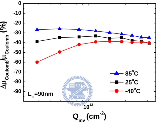
stressors under various temperatures. ………..…68 Fig. 3.18 The stress sensitivity of Coulomb mobility under various temperatures.
The Coulomb represents Coulomb_strain- Coulomb_neutral. ……….69
Fig. 3.19 Coulomb mobility versus Qinv with different bulk concentrations. It shows
model fits well with published data [23]. Both screened and unscreened Coulomb scattering effects are included in this model. ………..70 Fig. 3.20 Screened and unscreened Coulomb enhancement after 20% m* reduction.
The prior one shows +13% better than the latter one because of better screening effect by strain. ………71 Fig. 3.21 Coulomb mobility versus Qinv. 10% higher Qinv improves 13% Coulomb
due to better bulk screening effect. (Inset: Strain caused thinner inversion layer and then higher Qinv) ………..…72
Fig. 3.22 PFET low field mobility versus the vertical electric field at different LEFF
with neutral stressor. ………74 Fig. 3.23 Vertical field mobility sensitivity to temperature (EEFF=0.8MV/cm) versus
LEFF in PMOS. It shows that Coulomb mobility plays an important role in
the short channel region. When temperature is increased, the thermal velocity of carriers becomes faster. It means Coulomb scattering probability becomes lower and causes higher Coulomb mobility. ……..75 Fig. 3.24 Coulomb mobility data versus model in PMOS for long and short channel
regions. Coulomb mobility becomes smaller as LEFF shrinks because of
higher Na. A is a constant, α and β are both equal to 1, Na is extracted
from NCSU fitting programs. ………..76 Fig. 3.25 (a) PFET long channel mobility (LEFF=950nm) with neutral and
compressive CESL stressors. The mobility model matches with silicon data very well. Since the uniaxial stressor is only effective for short channel devices, the long channel mobility is almost the same under different neutral and compressive stressors. (b) PFET short channel mobility (LEFF=45nm) with neutral and compressive CESL stressors. The
room temperature.) ………..……78 Fig. 3.27 PFET total mobility versus EEFF after applying 230Mpa compressive
bending stress on devices with different LEFF. Unlike the behavior of local
stressors, significant mobility improvement can be observed from long to short channel devices in the high vertical field region because of global stress effect. (Inset: The schematic of the mechanical bending tool) ...79 Fig. 3. 28 PFET total mobility enhancement versus Qinv by applying compressive
mechanical stress on the devices with different LEFF. ……….80
Fig. 3.29 PFET Coulomb mobility versus Qinv by applying compressive mechanical
stress on the devices with different LEFF. No stress dependence is
observed for both long and short channel Coulomb mobility, which is consistent with the findings from local stressors. (Inset: Sxx represents the stress along the channel, Syy represents the stress vertical to the Si channel) ………81 Fig. 3. 30 PFET Coulomb mobility for short-channel devices with different stressors under various temperatures. ……….………82
Chapter 4
Fig. 4.1 Drain current with constant overdrive 1V with 21 samples for PFET. …94 Fig. 4.2 Drain current versus gate voltage at various temperatures for PFET with neutral stressor. ………95 Fig. 4.3 The characteristic of capacitance versus VG with various temperatures.
The CV curves are almost independent of temperature. ………..…96 Fig. 4.4 Extracted carrier mobility versus vertical electric field under various temperatures. ………97 Fig. 4.5 Extracted carrier mobility at EEFF=1.6MV/cm with various stressors. SR
dominates the total mobility for temperature <60K. ………98 Fig. 4.6 Mobility enhancement percentage () versus temperature with
scattering. ………..…………102 Fig. 4.10. SR/SR by biaxial strain extracted from the literature [3,4,28]. ……103
Fig. 4.11 NFET energy band diagram and electron repopulations showing that most electrons repopulate into 2 valley under biaxial tensile stress. It may result in higherΦb [24-27],heavier mz [24-27], shorterλand thus larger
SR . ………104
Fig. 4.12 NFET energy band diagram and electron repopulations showing that most electrons repopulate into 4‟ and 4‟‟ valley under uniaxial tensile stress. It may result in higherΦb,heavier mz, shorterλand thus larger SR ....105
Fig. 4.13 Hole subband versus different stress levels [2,24]. Uniaxial compressive and biaxial tensile have different subband splitting behavior. Zero energy represents the band edge of valence band. ………106 Fig. 4.14 PFET energy band diagram and hole repopulations with uniaxial
compressive stress and biaxial tensile stress. Subband energy levels are engineered with different stress types and most of hole carriers repopulate into the lower subband. (a) Uniaxial compressive stress increases mz and
Φb. Both factors improveλand then SR. (b) In the case of biaxial tensile
stress, when the Ge percentage is increased, the λ is initially increased by lighter mz but soon recovered due to higher Φb at high stress
levels...………107 Fig. 4.15 Wavefunction penetration into gate dielectric. ………..109 Fig. 4.16 Higher Φb and heavier mz show lower fraction f of carrier penetration
from 1D QM simulations. It is consistent with uniaxial-Tensile NFET in Table 4.1. ………110
Chapter 5
Fig. 5.1 Drain current versus gate voltage at various temperatures for PFETs with various stressors. The drain bias (VDS) is –5mV. The temperature
dependence of drain current shows strong correlation with stressor types. ………..……123 Fig. 5.2 The extracted carrier mobility shows significant dependence on the
Fig. 5.5 The measured total mobility with temperature ranging from 20K to 60K for neutral and compressive uniaxial stressors. The surface roughness mobility (SR) tends to dominate as EEFF>1.3MV/cm and is independent
of temperature. ………...127 Fig. 5.6 The extracted phonon scattering limited mobility for neutral and
compressive stressors at T=225K, 250K and 300K, respectively. …….128 Fig. 5.7 The EEFF dependence of SR. The extracted SR is proportional to
1.3 EFF
E .………129 Fig. 5.8 The EEFF dependence of PH. The extracted PH is proportional to
0.3 EFF
E .………130 Fig. 5.9 Temperature dependence of PH (T-α) for neutral and compressive
stressors.The α of neutral stressor is close to 1.75 [17], while the compressive stressor may further enhance the α value to around 2.3.…131 Fig. 5.10 Phonon temperature sensitivity should range from –1.5 to –3.13 for NFET and from –1.5 to –3.25 for PFET from empirical number [19]. Optical Phonon mobility dominates in the total phonon mobility at room temperature. ………132 Fig. 5.11 Schematic plot of E-k energy band diagram under uniaxial compressive stressor in PFET. Optical phonon energy (o) may increase when
Chapter 1
Introduction
1.1 Background and Motivation
For the past 50 years, the geometry scaling of silicon complementary metal-oxide semiconductor (CMOS) continues keep Moore‟s law effective by increasing in circuit integration density and also boosting transistor performance. In order to maintain Moore‟s law in nanoscale regime, the optimizations on the parasitic external resistance reduction and carrier mobility enhancement becomes more critical for the transistor design. For the past 25 years, global biaxial tensile strain technology has been widely developed to boost transistor mobility for both NMOSFET and PMOSFET [1]. This global biaxial strain technology is using a wafer-based approach of a thin strained Si layer on a thick relaxed Silicon-Gemanium (SiGe) virtual substrate. It is known that strain can improve phonon scattering limited mobility (PH) by reducing inter-valley
phonon scatterings and effective conduction mass [2]. However, the benefits of mobility enhancement only occur at low electric field and high stress level by this global strain [2]. Furthermore, the junction leakage induced by the lattice mismatch from silicon (Si) and gemanium (Ge) is also a barrier to implement the technique into mass production.
Recently, local uniaxial strained-Si technology becomes the preferred method to boost transistor mobility in nanoscale CMOS development and has been considered as a key process knob beyond 90nm technology [2-4]. The uniaxial strain process has the
significant mobility enhancement at both high field and low field region. (d) The uniaxial strain results in significantly smaller stress-induced threshold shift due to less bandgap narrowing. (e) Uniaxial strain provides better mobility enhancement than biaxial strain due to different band engineering mechanism and high stress levels.
Nevertheless, since the series resistance (Rsd) may counteract the actual mobility
enhancement in these strained devices, an accurate Rsd value has to be used in the
extraction of intrinsic effective mobility (eff). The most popular methods in the
determination of Rsd are the conventional Channel-Resistance method [5] and Shift &
Ratio method [6]. However, both methods are no longer suitable to nano-scale strained-silicon MOSFETs with halo implants because the laterally non-uniform halo doping as well as the uniaxial stress may result in a total resistance (Rtot) which does not
scale linearly with gate length [7,8]. It is difficult to determine Rsd accurately from the
non-linear Rtot vs. gate length characteristics. Therefore, an adequate method that may
accurately determine Rsd for nano-scale strained-silicon MOSFETs with halo implants is
sorely necessary.
It is known that uniaxial strain can improve phonon scattering limited mobility (PH) from band engineering and carrier repopulations [2]. However, because Coulomb
mobility (Coulomb) and surface roughness mobility (SR) dominate at low and high
vertical electric field (EEFF) respectively, whether uniaxial strain can improve Coulomb
enhanced in long-channel strained devices (L=10m). These findings seem to be inconsistent for biaxial strained MOSFETs, and further examination on Coulomb is
needed, especially for state of the art uniaxial strained MOSFETs.
Recently, the biaxial strain dependence of SR has been examined by Bonno et al.
[13] and Zhao et al. [14]. These studies show SR has strong strain sensitivity for both
nMOSFETs and pMOSFETs with biaxial strain. However, the observed SR data by
Zhao et al. [14] showed opposite trend between NFET and PFET and cannot be easily explained by the micro-roughness of Si/SiO2 interface. Furthermore, the uniaxial strain
dependence of SR has not been studied until now.
Besides, the temperature effect on strain-enhanced mobility is of special importance because it may provide insights for the underlying mechanisms responsible for the performance enhancement. Several studies have investigated the temperature effect on strain-enhanced mobility in the past [15-18]. For NMOS, the temperature effect of process-induced biaxial strain [15,16], uniaxial strain [15] and mechanical uniaxial strain [17] applied on devices has been experimentally studied. The results all indicated less strain sensitivity in carrier mobility with decreasing temperature due to less contribution of the intra valley scatterings in the 4-fold valleys. For PMOS, the temperature effect of process-induced biaxial strain [16] and mechanical uniaxial strain [18] has also been investigated. The results showed higher strain sensitivity in carrier mobility with decreasing temperature due to lighter effective conduction mass, i.e., the
finding in this work [19], the strain-enhanced temperature sensitivity of PH, has
unveiled the underlying mechanism responsible for these observations.
1.2 Organization
This dissertation includes six chapters.
In Chapter 1, the background and the motivation of this thesis are discussed. In Chapter 2, we introduce the BSIM-based method for the Rsd extraction [20].
Using this method, Rsd can be well extracted in nano-scale strained devices. We have
verified this method using samples with different process conditions and good agreement with experimental data has been obtained. This BSIM-based method is also verified by TCAD simulated current-voltage (IV) characteristics [21]. The extracted Rsd
will be used in the following chapters for the extraction of carrier mobility.
In Chapter 3, by using the split-CV method [22], the channel mobility in the short channel devices can be extracted by calibrating the extracted Rsd values from Chapter 2,
as a shown in Fig. 1.1. Then we assessed the impact of process-induced uniaxial strain on Coulomb mobility in short-channel nMOSFETs and pMOSFETs under various temperatures [23,24]. We also utilized the four-point mechanical bending technique on both short and long channel devices in PMOSFETs. Our study indicates that the stress sensitivity of the Coulomb mobility shows strong temperature dependence due to the competition result of the stress sensitivity between bulk charge scattering and interface
Furthermore, the SR has higher strain dependence than the phonon scattering limited
mobility (PH). Our experimental results confirm the previously reported results based
on simulations [27,28] In addition, a wavefunction penetration perspective [29,30] is proposed to explain the possible physical origin of the uniaxial strain dependence of SR.
In Chapter 5, we conduct an experimental assessment for the impact of process-induced uniaxial strain on the temperature dependency of carrier mobility in nanoscale pMOSFETs [31]. Furthermore, through cryogenic temperature measurement from Chapter 4, we investigate the impact of uniaxial strain on the temperature dependence of phonon-scattering limited mobility in nanoscale PMOSFETs [19]. The EEFF and temperature dependence of the extracted SR and PH will be discussed and
benchmarked with published data [32,33]. Our study indicates that the strain sensitivity of hole mobility becomes less with increasing temperature and it is consistent with previous uniaxial mechanical bending result [18]. The temperature sensitivity of phonon mobility becomes higher when compressive strain is applied. It can be explained by the higher optical phonon energy induced by uniaxially-compressive strain. Our new findings also explain the higher temperature sensitivity of drain current presented in uniaxial strain PMOSFETs.
In Chapter 6, we summarize the key research results and the contribution of this thesis.
References
[1] M. V. Fischetti, and S. E. Laux, “Band structure, deformation potentials, and carrier mobility in strained Si, Ge, and SiGe alloys,” J. Appl. Phys., vol. 80(4), pp. 2234-2252, August 1996.
[2] Scott E. Thompson, Guangyu Sun, Youn Sung Choi and Toshikazu Nishida, “Uniaxial-Process-Induced Strained-Si: Extending the CMOS Roadmap,” IEEE
Transactions on Electron Devices vol. 53(5), pp. 1010-1020, May 2006.
[3] Z. Luo, N. Rovedo, S. Ong, B. Phoong, M. Eller, H. Utomo, C. Ryou, H. Wang, R. Stierstorfer, L. Clevenger, S. Kim, J. Toomey, D. Sciacca, J. Li, W. Wille, L. Zhao, L. Teo, T. Dyer, S. Fang, J. Yan, O. Kwon, D. Park, J. Holt, J. Han, V. Chan, J. Yuan, T. Kebede, H. Lee, S. Kim, S. Lee, a. Vayshenker, Z. Yang, C. Tian, H. Ng, H. Shang, M. Hierlemann, J. Ku, J. Sudijono, M. Ieong, “High Performance Transistors Featured in an Aggressively Scaled 45nm Bulk CMOS Technology,” Symp. VLSI Tech., pp. 16-17, June 2007.
[4] S. E. Thompson, M. Armstrong, C. Auth, M. Alavi, M. Buehler, R. Chau, S. Cea, T. Ghani, G. Glass, T. Hoffman, C. H. Jan, C. Kenyon, J. Klaus, K. Kuhn, Z. Ma, B. Mcintyre, K. Mistry, A. Murthy, B. Obradovic, R. Nagisetty, P. Nguyen, S. Sivakumar, R. Shaheed, L. Shifren, B. Tufts, S. Tyagi, M. Bohr, and Y. E. Mansy, “A 90-nm Logic Technology Featuring Strained-Silicon,” IEEE Transactions on Electron Devices vol. 51(11), pp. 1790-1797, November 2004.
[7] D. Esseni, H. Iwai, M. Saito, and B. Ricco, “Nonscaling of MOSFET‟s Linear Resistance in the Deep Submicrometer Regime,” IEEE Electron Device Letter, vol. 19(4), pp. 131-133, April 1998.
[8] Hans van Meer, Kirklen Henson, Jeong-Ho Lyu, Maarten Rosmeulen, Stefan Kubicek, Nadine Collaert, and Kristin De Meyer, "Limitations of Shift-and Ratio Based Leff Extraction Techniques for MOS Transistors with Halo or Pocket Implants,” IEEE
Electron Device Letters, vol. 21(3), pp. 133-136, March 2000.
[9] Olivier Weber, and Shin-ichi Takagi, “New Findings on Coulomb Scattering Mobility in Strained-Si nFETs and its Physical Understanding,” Symp. VLSI Tech., pp. 130-131, June 2007.
[10] Hasan M. Nayfeh, Christopher W. Leitz, Arthur J. Pitera, Eugene A. Fitzgerald, Judy L. Hoyt, and Dimitri A. Antoniadis, “Influence of High Channel Doping on the Inversion Layer Electron Mobility in Strained Silicon n-MOSFETs,” IEEE Electron
Device Letters, vol. 24(4), pp. 248-250, April 2003.
[11] F. Gamiz, J. B. Roldan, J.A. Lopez-Villanueva, and P. Cartujo, “Coulomb scattering in strained-silicon inversion layers on Si1-xGex substrates,” Appl. Phys. Lett.,
vol. 69(6), pp. 797-799, August 1996.
[12] Antoine Cros, Krunoslav Romanjek, Dominique Fleury, Samuel Harrison, Robin Cerutti, Philippe Coronel, Benjamin Dumont, Arnaud Pouydebasque, Romain Wacquez, Blandine Duriez, Romain Gwoziecki, Frederic Boeuf, Hugues Brut, Gerard Ghibaudo, Thomas Skotnicki, “Unexpected mobility degradation for very short devices: A new
Morphology,” Symp. VLSI Tech., pp. 134-135, June 2007.
[14] Y. Zhao, H. Matsumoto, T. Sato, S. Koyama, M. Takenaka and S. Takagi, “A Novel Characterization Scheme of Si/SiO2 Interface Roughness for Surface Roughness Scattering-Limited Mobilities of Electrons and Holes in Unstrained- and Strained-Si MOSFETs,” IEEE Transactions on Electron Devices, vol. 57(9), pp. 2057-2066, September 2010.
[15] F. Lime, F. Andrieu, J. Derix, G. Ghibaudo, F. Boeuf, and T. Skotnicki, “Low temperature characterization of effective mobility in uniaxially and biaxially strained nMOSFETs,” Solid-State Electronics, vol. 50(4), pp. 644-649, April 2006.
[16] Nobuyuki Sugii and Katsuyoshi Washio, “Low-Temperature Electrical Characteristics of Strained-Si MOSFETs,” Jpn. J. Appl. Phys., Part 1, vol. 42, pp. 1924-1927, 2003.
[17] M. N. Tsai, T. C. Chang, P. T. Liu, O. Cheng, and C. T. Huang, “Temperature Effects of n-MOSFET Devices with Uniaxial Mechanical Strains,” Electrochemical and
Solid-State Letters, vol. 9(8), pp. 276-278, June 2006.
[18] Xiaodong Yang, Srivatsan Parthasarathy, Yongke Sun, Andrew Koehler, Toshikazu Nishida, and Scott E. Thompson, “Temperature dependence of enhanced hole mobility in uniaxial strained p-channel metal-oxide-semiconductor field-effect transistors and insight into the physical mechanisms,” Applied Physics Letter vol. 93(24), pp. 243503-243503-3, December 2008.
Extraction Method in Nanoscale MOSFETs,” Journal of The Electrochemical Society, vol. 156(1), H34-H38, 2009.
[22] K. Romanjek, F. Andrieu, T. Ernst, and G. Ghibaudo, “Improved Split C-V Method for Effective Mobility Extraction in sub-0.1-m Si MOSFETs,” IEEE Electron
Device Letters, vol. 25(8), pp. 583-585, August 2004.
[23] William P.-N. Chen, P. Su, K. Goto, “Investigation of Coulomb Mobility in Nanoscale Strained PMOSFETs,” IEEE Transactions on Nanotechnology, vol. 7(5), pp. 538-543, September 2008.
[24] William P.-N. Chen, P. Su, K. Goto, “Impact of Process-Induced Strain on Coulomb Scattering Mobility in Short-Channel n-MOSFETs,” IEEE Electron Device
Letters, vol. 29(7), pp. 468-470, July 2008.
[25] Kenneth Chain, Jian-Hui Huang, Jon Duster, Pin K Ko and Chenming Hu, “A MOSFET electron mobility model of wide temperature range (77-400K) for IC simulation,” Semiconductor Science Technology, vol. 12(4), pp. 355-358, 1997.
[26] William P.N. Chen, Jack J.-Y. Kuo, and Pin Su, “Experimental Investigation of Surface Roughness Limited Mobility in Uniaxial Strained pMOSFETs,” IEEE Electron
Device Letters, in press.
[27] M. V. Fischetti, F. Gamiz, and W. Hansch, “On the enhanced electron mobility in strained-silicon inversion layers,” J. Appl. Phys., vol. 92(12), pp. 7320-7324, December 2002.
[29] I. Polishchuk and C. Hu, “Electron Wavefunction Penetration into Gate Dielectric and Interface Scattering- An Alternative to Surface Roughness Scattering Model”, Symp.
VLSI Tech, pp. 51-52, June 2001.
[30] William P.N. Chen, Jack J.-Y. Kuo, Barney K-.Y. Lu and Pin Su, “Experimental Investigation and Modeling for Surface Roughness Limited Mobility in Strained pMOSFETs”, Extended Abstracts of the 2010International Conference on Solid State
Devices and Materials (SSDM), Tokyo, Japan, pp. 49-50, September 2010.
[31] William P.N. Chen, Jack J.-Y. Kuo, and Pin Su, “Impact of Process-Induced Uniaxial Strain on the Temperature Dependence of Carrier Mobility in Nanoscale pMOSFETs,” IEEE Electron Device Letters, vol. 31(5), pp. 414-416, May 2010.
[32] Shin-ichi Takagi, Akira Toriumi, Masao Iwasw, and Hiroyuki Tango, “On the Universality of Inversion Layer Mobility in Si MOSFET‟s: Part II – Effects of Surface Orientation,” IEEE Transactions on Electron Devices, vol. 41(12), pp. 2363-2368, December 1994.
[33] Kwyro Lee, Joo-Sun Choi, Sang-Pil Sim and Choong-Ki Kim, “Physical Understanding of Low-Field Carrier Mobility in Silicon MOSFET Inversion Layer,”
CV measurement with Covcalibration
Id-VG measurement
Rsd& ideal drain current Inversion charge &
bulk charge Channel mobility BSIM
CdV
Q
ds inv effV
Q
L
W
I
L
L
L
eff
TEM
CV measurement with Covcalibration Id-VG measurementRsd& ideal drain current Inversion charge &
bulk charge Channel mobility BSIM
CdV
Q
ds inv effV
Q
L
W
I
L
L
L
eff
TEM
Chapter 2
A New Series Resistance Extraction Method for
Nanoscale MOSFETs
2.1 Introduction
As strained-silicon and USJ (Ultra Shallow Junction) techniques are widely used to optimize the carrier velocity and parasitic resistances in the MOSFET, an accurate determination of the parasitic source/drain series resistance (Rsd) for these nano-scale
MOSFETs becomes a crucial issue. Since the series resistance may counteract the mobility enhancement in these strained devices, an accurate Rsd value has to be used in
the extraction of intrinsic effective mobility (eff) during process development.
Furthermore, the Rsd parameter is critical to evaluate the performance of USJ
engineering works.
Among several studies regarding the Rsd extraction in the past [1]-[4], Kim et al. [1]
proposed an integrated methodology to separate Rsd components and utilized the
conventional Channel-Resistance method in the determination of Rsd. Although the
Channel-Resistance method has been widely used [1]-[2], it is no longer suitable to nano-scale strained-silicon MOSFETs with halo implants because the laterally non-uniform channel doping as well as the uniaxial stress may result in a total resistance
devices [6]. Therefore, an adequate method that may accurately determine Rsd for
nano-scale strained-silicon MOSFETs with halo implants is sorely needed.
In this work, we tackle this problem by a BSIM-based method [7]. Using this method, Rsd can be well extracted in nano-scale strained devices. The extracted Rsd will
be used in the following chapters for the extraction of carrier mobility.
2.2 Devices and Experimental Setup
The devices used in this experiment were fabricated by state-of-the art IC manufacturing technology [10], which provides transistors with gate lengths ranging from 4m down to 41nm with same channel width (W = 1m) on 300mm bulk substrate. A 1.2nm nitrided gate oxide was used as a gate dielectric. Processes with ultra low HDE (Highly Doped Extension) energy and unique Spike Rapid Thermal Annealing condition were used to maintain good SCE (Short Channel Effect) control and high activation rate simultaneously. In this study, devices with different extension dosage and various stressors (Tensile/Compressive/Neutral) in NMOS were adopted to verify this extraction methodology. The testkeys constituted by the transistor arrays and calibration patterns are designed for CV measurement. Transistor arrays with Source/Drain tied together can provide enough area to characterize the capacitance in nano-scale devices. Moreover, we have used a high frequency probing system to improve the accuracy and stability of CV characterization results.
2.3 Methodology and Discussion
the channel. This effect is so called bulk charge effect. Abulk is very close to 1 if the
channel length is short. Since the effective channel length (Leff) plays a crucial role in
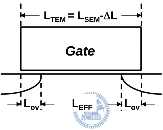
the extraction of Rsd, it needs to be adequately determined first. Leff can be calculated by
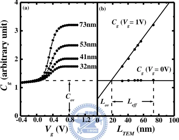
(LTEM - 2Lov) as depicted in Fig. 2.2 LTEM may be obtained from the in-line SEM
(Scanning Electron Microscopy) measurement (with accuracy within ± 2nm) at poly patterned stage and the etching-induced length bias(L). Lov represents the overlap
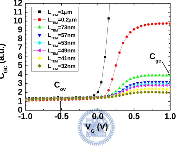
distance between source/drain and gate and can be extracted from CV (Capacitance-Voltage) measurement [11,12]. Fig. 2.3 shows the CV curves of different LTEM in NMOS. Cgc and Cov can be extracted at gate bias equal to 1.0V and –0.5V
respectively [11]. The gate length dependency of extracted Cgc and Cov is shown in Fig.
2.4. Lov can be easily obtained from the intercept of Cgc and Cov [11,12].
Since the conventional Rsd extraction methods, which do not consider the gate
length dependency of eff, need to conduct the Rsd extraction using devices with gate
length ranging from short to long channel, their extraction errors are significant. Therefore, in this work, we carried out the Rsd extraction based on the nano-scale
devices with LTEM from 50nm to 83nm.
For these short-channel devices, the impact of Rsd on the drain current (Id) in the
0 0 1 E Eeff eff
nm L TEM sd sd TEM TEM Si sd TEM Id L E R R E L Id L Id R E 83 ~ 50 model 0 0 0 0 model 0 0 min ' , ' , ' , ' , ' , ' , ' , ' , ) ( ) ' , ' , ' , ' ( Note that Eq. (1) can be derived from the BSIM drain current model [7] under the assumption that the carrier velocity saturation and the bulk-charge effect are negligible.
The effective mobility (eff) in Eq. (1) can be modeled by [7]
(2)
where 0, E0 and are model fitting parameters. Eeff represents the average electric field
experienced by the carriers in the inversion layer and is given by (Vg + Vth) / 6Tox for an
NMOS transistor with n-type poly-silicon gate.
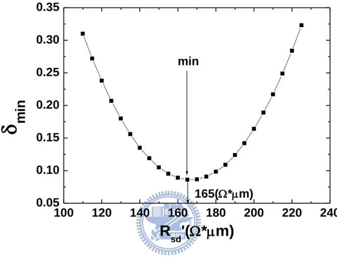
Since the accuracy of Eq. (1) in fitting the experimental data strongly depends on Rsd, we propose to determine Rsd by the following objective function:
(3)
where Idsi and Idmodel represent the measured drain current and the calculated Id by Eq.
(1), respectively. 0 ‟
, E0 ‟
and υ‟ are the optimized model parameters that may result in a minimum model-hardware discrepancy (δmin) for a given Rsd‟. The correlation of δ min and Rsd‟ shown in Fig. 2.5 indicates thatδmin is sensitive to the change in Rsd‟ and we
Note that if the Rsd value is not accurate, the drain current ratio of devices with different
LTEM will not be correct, as shown in Fig. 2.6. Fig. 2.7 provides the Rsd sensitivity with
variations on different key parameters, where Rsd is the most sensitive to Leff but this
can be overcome by careful in-line measurement. It is worth noting that the variation in eff has to be limited to within ± 5% if ± 4% Rsd variation is the maximum tolerance
level. In this work, we carried out the Rsd extraction based on the devices with LTEM
from 50nm to 83nm, where the variation of eff is within ± 5%.
To test our Rsd extraction methodology, NMOS and PMOS transistors with various
extension conditions have been used. Fig. 2.8 shows the relationship between Rsd and
the measured overlap capacitance (Cov) for these devices. It can be seen that when we
increase the extension dose and hence the overlap distance (Lov), the extracted Rsd
indeed decreases as Cov increases. Rsd values of PMOS are around two times of NMOS.
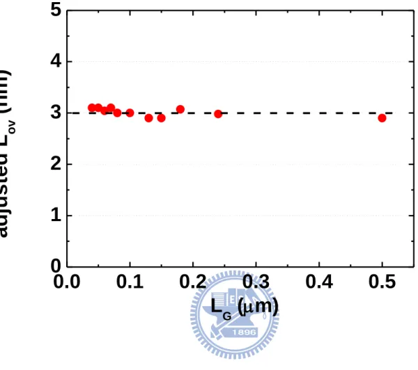
We assume Rsd is independent of LTEM due to the following observations: (i) In Fig.
2.8, Rsd is very sensitive to overlap capacitance (Cov). However, Fig. 2.4 shows that Cov
is independent of LTEM. (ii) Based on our Tsuprem4 simulation results incorporated with
halo implants, the Lov (Extension overlap distance under the poly) is independent on
LTEM, as shown in Fig. 2.9.
Once Rsd is accurately determined, the intrinsic eff may be obtained using Eq. (1).
Several explanations regarding the mobility degradation behavior in the short channel regime were proposed in the past, including halo implants and quasi-ballistic transport characteristics performed in these nano-scale devices [2,14,15]. This issue, nevertheless, deserves further study in the future. Using the extracted eff (LTEM) in Eq. (1), good
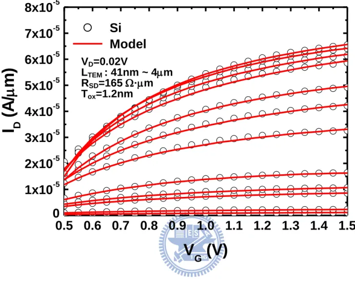
agreement with the silicon data over a wide range of LTEM (41nm to 4m) can be seen,
as shown in Fig. 2.11.
Please note eff extracted here is based on the charge density (Qinv) approximated
by Cox×(Vg-Vth). However, some channel charge still exists in the sub-threshold region.
The better approach to obtain the Qinv result is a direct measurement of Qinv (split-CV
method) from capacitance measurement, with the mobile channel charge density determined from the gate-to-channel capacitance (Cgc), as shown in Eq. (4):
gs V V gc inv
C
dV
Q
gs fb
(4)We will leave it for the detail discussions in chapter 3.
2.4 Verification by TCAD Simulation
To verify the proposed BSIM Rsd extraction method, we extract Rsd from simulated
Id-Vg curves by Medici simulator [16] and compare with Rsd obtained from the ohmic
drop in the source region of the simulated device structures. The drain bias condition is set to 50mV. Three values of specific resistivity (7x10⁻⁸, 1x10⁻⁷ and 1.3x10⁻⁷*cm2) are input to modify Rsd values and then the related Id-Vg characteristics are generated for
extracted directly. Rsd here is defined as Rsd (c)- Rsd (c=1x10⁻⁷*cm2). As shown in
Fig. 2.12, Rsd extracted from potential contour with different specific resistivity values
shows the consistent trend with Rsd extracted by BSIM fitting method. It indicates that
the proposed BSIM method can accurately quantify the difference of Rsd and be a
suitable monitor tool for USJ (Ultra Shallow Junction) and strained process development.
2.5 Conclusion
We have proposed a BSIM-based method for Rsd and eff extraction which applies
to nano-scale strained-silicon MOSFETs with halo implants. This Rsd extraction method
may serve as a suitable process monitor tool for USJ (Ultra Shallow Junction) and strained process development. This method is more accurate than the conventional Channel-Resistance and Shift & Ratio method because it considers the gate-length dependence of mobility caused by local uniaxial stress and laterally non-uniform channel doping. We have verified this method using samples with different stressor/doping conditions and good agreement with experimental data has been obtained. Significant mobility degradation in short channel regime has been observed for various uniaxial stressors. The accuracy of BSIM Rsd extraction method is also
verified by simulated IV characteristics with different external resistant values in short channel region. Therefore, this method may serve as a suitable process monitor tool for
References
[1] S.D. Kim, S. Narasimha, K. Rim, “An Integrated Methodology for Accurate Extraction of S/D Series Resistance Components in Nanoscale MOSFETs,” IEDM Tech.
Dig., pp. 149-152, December, 2005.
[2] K. Romanjek, F. Andrieu, T. Ernst, G. Ghibaudo, “Characterization of the effective mobility by split C(V) technique in sub 0.1 m Si and SiGe PMOSFETs,” Solid-State
Electronics, vol. 49(5), pp. 721-726, May 2005.
[3] Yuan Taur, “MOSFET Channel Length: Extraction and Interpretation,” IEEE
Transactions Electron Devices, vol. 47(1), pp. 160-170, January 2010.
[4] Abhisek Dixit, Anil Kottantharayil, Nadine Collaert, Mike Goodwin, Malgorzata Jurczak, Kristin De Meyer, “Analysis of the Parasitic S/D Resistance in Multiple-Gate FETs,” IEEE Transactions Electron Devices, vol. 52(6), pp. 1132-1140, June 2005. [5] D. Esseni, H. Iwai, M. Saito, and B. Ricco, “Nonscaling of MOSFET‟s Linear Resistance in the Deep Submicrometer Regime,” IEEE Electron Device Letter, vol. 19(4), pp. 131-133, April 1998.
[6] Hans van Meer, Kirklen Henson, Jeong-Ho Lyu, Maarten Rosmeulen, Stefan Kubicek, Nadine Collaert, and Kristin De Meyer, "Limitations of Shift-and Ratio Based Leff Extraction Techniques for MOS Transistors with Halo or Pocket Implants,” IEEE
Electron Device Letters, vol. 21(3), pp. 133-136, March 2000.
[7] Y. Cheng and C. Hu, “MOSFET Modeling & BSIM3 User‟s Guide,” KAP (1999) [8] William P.N. Chen, Pin Su, K. Goto, C. Diaz, “Series Resistance and Mobility
Nano-Scale MOSFETs”, VLSI-TSA-Tech, pp.143-144, April 2006.
[10] Samuel K. H. Fung et al., “65nm CMOS High Speed, General Purpose and Low Power Transistor Technology for High Volume Foundry Application,” Symp. VLSI
Tech., pp. 92-93, June 2004.
[11] K. Romanjek, F. Andrieu, T. Ernst, and G. Ghibaudo, “Improved Split C-V Method for Effective Mobility Extraction in sub-0.1-m Si MOSFETs,” IEEE Electron
Device Letters, vol. 25(8), pp. 583-585, August 2004.
[12] Dieter K. Schroder, “ Semiconductor Material and Device Characterization,” 3rd edition, A John Wiley & Sons, INC., Publication (2006).
[13] http://www.itrs.net/Links/2006Update/2006UpdateFinal.htm, ITRS 2006 Update,
Process Integration, Devices, and Structures, p.9 (2006)
[14] Chu Hao, B. Cabon-Till, S. Cristoloveanu, G. Ghibaudo, “Experimental Determination of Short-Channel MOSFET Parameters,” Solid-State Electronics, vol. 28(10), pp. 1025-1030, October 1985.
[15] Antoine Cros, Krunoslav Romanjek, Dominique Fleury, Samuel Harrison, Robin Cerutti, Philippe Coronel, Benjamin Dumont, Arnaud Pouydebasque, Romain Wacquez, Blandine Duriez, Romain Gwoziecki, Frederic Boeuf, Hugues Brut, Gerard Ghibaudo, Thomas Skotnicki, “Unexpected mobility degradation for very short devices: A new challenge for CMOS scaling,” IEDM Tech. Dig., pp. 1-4, December 2006.
Characterization
(Linear I
DV
G, t
ox, V
th)
Input Initial R
sdOptimized R
sd&
eff(
0,E
0,
)? [Fig.5]
N
Unique R
sdobtained
[Fig.6]
Y
Fit I
DV
Gin small range of L
Gby
tuning
eff(
0,E
0,
)
L
Gdependency of intrinsic
eff(
0,E
0,
) obtained [Fig.10]
Adjust
R
sdL
EFFExtraction
Characterization
(Linear I
DV
G, t
ox, V
th)
Input Initial R
sdOptimized R
sd&
eff(
0,E
0,
)? [Fig.5]
N
Unique R
sdobtained
[Fig.6]
Y
Fit I
DV
Gin small range of L
Gby
tuning
eff(
0,E
0,
)
L
Gdependency of intrinsic
eff(
0,E
0,
) obtained [Fig.10]
Adjust
R
sdParameter Table Symbol Definition ID Drain current in linear region
Cgc Gate oxide capacitance
Lov Gate-extension overlap distance; extracted from Cgc and Cov LTEM
Obtained from LSEM- L. LSEM is from in-line measurement.
L is a constant offset between LTEM and LSEM Leff LTEM-2*Lov
eff Effective mobility; Need to calibrate with Rsd by iterations Vth Threshold voltage from measurement
Abulk Bulk charge parameter; Abulk~1 in short channel region
Esat Saturation electrical field; Set Esat~
so that Vds/Esat*Leff<<10
E0
Rsd Source/Drain series resistance
Input Parameter
Mobility fitting parameter
Fitting Parameter
L
TEM
= L
SEM
-
L
L
EFF
L
ov
Gate
L
ov
L
TEM
= L
SEM
-
L
L
EFF
L
ov
L
ov
Gate
L
ov
L
ov
-1.0
-0.5
0.0
0.5
1.0
0
1
2
3
4
5
6
7
8
9
10
11
12
C
gcC
ovC
GC(
a
.u
.)
V
G(V)
L TEM=1m L TEM=0.2m L TEM=73nm L TEM=57nm L TEM=53nm L TEM=49nm L TEM=41nm L TEM=32nmFigure 2.3. The measured CV curves in NMOS with various LTEM. Cgc & Cov are
0
20
40
60
80
100
0
1
2
3
4
5
L
eff2*L
ovC
ovC
gcC
gc&
C
ov(
a.
u
.)
L
TEM(nm)
Figure 2.4. Plot of Cgc & Cov versus various LTEM. Lov and Leff can be obtained
100
120
140
160
180
200
220
240
0.05
0.10
0.15
0.20
0.25
0.30
0.35
min
165(
*
m)
m
in
R
sd'(
*
m)
Figure 2.5. The objective function, min, versus Rsd‟. Optimized Rsd (165 *m)
0.5 0.6 0.7 0.8 0.9 1.0 1.1 1.2 1.3 1.4 1.5
0
1x10
-52x10
-53x10
-54x10
-55x10
-56x10
-57x10
-58x10
-5I
D
(
A
/
m)
V
G(V)
Si
Model(R
sd:165
*
m)
Model(R
sd:110
*
m)
V
D= 0.02V
L
TEM= 50nm~83nm
R
sd=165
·
m
Figure 2.6. Id-Vg modeling results using various Rsd values. The three groups of
curves correspond to different gate length ranging from 50nm to 83nm. If the Rsd
value in the model is not accurate (e.g., Rsd = 110 *m), the drain current ratio
0
1
2
3
4
5
6
7
8
9
10
-15
-10
-5
0
5
10
15
L
GV
thC
ovt
ox
R
sd
v
a
ri
a
ti
o
n
(
%
)
Parameter variation (%)
0.20
0.25
0.30
0.35
0.40
0
100
200
300
400
500
600
R
sd(o
h
m
/
m)
C
ov(fF/
m)
NMOS
PMOS
0.0
0.1
0.2
0.3
0.4
0.5
0
1
2
3
4
5
adj
usted
L
ov(n
m)
L
G(
m)
Figure 2.9. Lov (Extension overlap distance under poly) versus LG from Tsuprem4
0.01
0.1
1
10
-80
-60
-40
-20
0
20
40
60
NMOS
189
-
m
195
-
m
185
-
m
n
o
rm
a
li
z
e
d
eff(
c
m
2/V
-s
)
L
TEM(
m)
Tensile
Compress
Control
V
D=0.02V
E
eff=1.8MV/cm
L
TEM: 41nm ~ 4
m
T
ox=1.2nm
Figure 2.10. eff(LTEM) for NMOS devices with halo implants and various stressors
(Tensile/0 stress/Compressive). The mobility is subtracted by a positive constant for normalization purpose.
0.5 0.6 0.7 0.8 0.9 1.0 1.1 1.2 1.3 1.4 1.5
0
1x10
-52x10
-53x10
-54x10
-55x10
-56x10
-57x10
-58x10
-5Si
Model
I
D(
A
/
m)
V
G(V)
V
D=0.02V
L
TEM: 41nm ~ 4
m
R
SD=165
·
m
T
ox=1.2nm
Figure 2.11. Id-Vg modeling results for a wide range of LTEM using the extracted
Figure 2.12. A comparison plot of Rsd versus c (specific resistivity) with two Rsd
extraction methods - BSIM fitting method and Medici potential contour method. Rsd equals to Rsd (c)- Rsd (c=1x10⁻⁷*cm2). (Inset: potential contour of
simulation MOSFET profile, Rsd is extracted by Ohm‟s law: (VA-VB)/Id).
6.0x10
-88.0x10
-81.0x10
-71.2x10
-71.4x10
-71.6x10
-7-40
-30
-20
-10
0
10
20
30
40
R
sd(o
hms)
c(ohms*cm
2)
Potential Drop BSIM Method VA V B Source Silicide P o ly VA V B Source Silicide P o ly NMOS VD=0.05V LTEM=80,90,100nmChapter 3
Investigation of Coulomb Mobility in Nanoscale
Strained MOSFETs
3.1 Introduction
Uniaxial strained-Si technology is critical to transistor performance in nanoscale CMOS development [1-2]. The improvement of current drive shows strong correlation with the low-field mobility enhancement by uniaxial strain [3]. However, in order to suppress the short channel effect for device scaling, halo implantation is widely used. With shrinking gate length, halo profiles begin to merge and result in higher effective bulk concentration. Recently, several studies [4-9] reported degraded carrier mobility for short channel devices and pointed out the increasing importance of Coulomb scatterings. Whether or not the Coulomb scattering mobility can be enhanced by process-induced strain is crucial to device design and merits investigation.
Although Gamiz et al. [6] and Nayfeh et al. [5] have shown that Coulomb mobility is not enhanced in strained-Si nMOSFETs, Weber and Takagi [4] have demonstrated that the mobility limited by substrate impurity scattering is still enhanced in long-channel strained devices (L=10m). These findings seem to be inconsistent, and further examination on Coulomb mobility is needed. Furthermore, similar studies have
nMOSFETs and pMOSFETs. The Coulomb mobility in the short channel region under compressive and neutral uniaxial local stress conditions is carefully characterized by split C-V (Capacitance-Voltage) method and Matthiessen‟s rule. In order to further verify our experimental results, we have also utilized the four-point mechanical bending technique on both short and long channel devices in PMOSFETs.
3.2 Devices and Experimental
For comparison purpose, N-channel and P-channel MOSFETs with channel direction <110> with neutral and compressive uniaxial Contact Etch Stop Layer (CESL) were manufactured based on state-of-the-art CMOS technology on 300mm (100) silicon substrate, as shown in Fig. 3.1. The compressive film may transfer significant compressive stress to the channel region, modulating silicon subbands and carrier populations, and altering carrier mobility [14]. In Fig. 3.2 (a) and (b), the device on-off performance is boosted –36% and +35% by compressive uniaxial stressors in the short channel region for NMOSFETs & PMOSFETs, respectively.
The devices with neutral and compressive CESL films were implanted by the same pocket conditions. Shallow Trench Isolation (STI) was patterned to define the active region. Then an ultra thin oxide was grown on the surface of wafer. The poly gate was implanted with heavily doped N/P type species after poly deposition and post annealed to increase gate activation rates. Then ultra shallow HDD (Highly Doped Drain) implant, spacer formation, source and drain implant, post implantation annealing, and back-end process were implemented sequentially.