國 立 交 通 大 學
電 機 與 控 制 工 程 學 系
博 士 論 文
具輸入電流修飾與柔性切換特性的單級交流-直流轉換器
Single-Stage AC-DC Converters with Input Current Shaping and
Soft-Switching Features
研
究 生 : 劉 晏 銘
指 導 教 授 : 張 隆 國
博 士
具輸入電流修飾與柔性切換特性的單級交流-直流轉換器
Single-Stage AC-DC Converters with Input Current Shaping and Soft-Switching Features
研 究 生 : 劉 晏 銘 Student: Yen-Ming Liu
指 導 教 授 : 張 隆 國 Advisor: Lon-Kou Chang
國 立 交 通 大 學
電 機 與 控 制 工 程 學 系 博 士 論 文
A Dissertation
Submitted to Department of Electrical and Control Engineering College of Electrical Engineering
National Chiao Tung University in Partial Fulfillment of the Requirements
for the Degree of Doctor of Philosophy
in
Electrical and Control Engineering August 2007
Hsinchu, Taiwan, Republic of China.
具輸入電流修飾與柔性切換特性的單級交流-直流轉換器
研究生:劉晏銘
指導教授:張隆國 博士
國立交通大學電機與控制工程學系
摘要
本論文旨在發展出具新穎性的單級交流-直流轉換電路以提升整體效能
並符合成本效益,這些設計都是基於減低諧波污染的前提下所設計的,並
可滿足如
IEC 61000-3-2 等電流諧波標準規範。
一般使用升壓型輸入電流修飾設計的的單級交流-直流轉換器常見的問
題包括:開關電流應力過大並帶來額外的開關功率損失,以及使用電壓隨
耦功因修正技術造成的輸入線電流失真。我們除了使用主動箝位的電路設
計外,較新穎部分的解決策略分別為:改讓升壓電感在開關截止時做充磁
以減緩開關導通時的電流應力和功率損耗;以及,輸入電流修飾子電路配
合輸入線電壓的瞬間值自動調整其充磁時間,使得升壓電感的充磁電流得
以補償放磁電流所造成的非線性失真,以此設計,輸入側的電流-電壓曲線
可得到近乎線性的關係。
另一個需要面對的關鍵問題則是儲能電容電壓應力過大。本論文對此
提出一個新型的單級交流-直流轉換器,此架構使用一反馳式與順向式整合
型電路作為直流-直流輸出調整器。在此架構中,反馳式與順向式子轉換器
分別被操作在連續導通模式與非連續導通模式之下。因此,在輕載的情況
下,藉由抑止反馳式並維持順向式的正常運作即可利用非連續導通模式的
輸出特性有效地抑制儲能電容電壓,並能保證在各種工作情況下都低於一
般電容的最大電壓容忍值
450 V。
本文中所提出的技術皆已在泛用型輸入電源(90–260 Vrms)的測試條
件下實證過,實驗結果證明本文所提出的設計可有效地解決電流應力過
大、電壓應力過大與轉換效率不佳的問題。
Single-Stage AC-DC Converters with Input Current Shaping
and Soft-Switching Features
Student: Yen-Ming Liu
Advisor: Dr. Lon-Kou Chang
Department of Electrical and Control Engineering
National Chaio Tung University
Abstract
This dissertation presents innovative techniques and solutions to simultaneously improve the performance and satisfy the cost-effective consideration for the single-stage input current shaping (S2ICS) AC-DC converters. These designs are based on the consideration for limiting the line current harmonics, especially for meeting the stringent current harmonic regulations, such as IEC 61000-3-2.
For general S2ICS converters employing boost-type input current shaping (ICS) cells, these circuits usually suffer from the relatively high switch current stress and line current waveform distortion caused by the voltage-follower control. To remedy these drawbacks, this dissertation presents a novel ICS technique for S2ICS converters. Unlike the conventional single-stage designs, the proposed ICS scheme is intentionally arranged to be charged in the duty-off time. With this design, the switch current stress in the duty-on time is significantly mitigated and accordingly the power loss is reduced. Moreover, this design produces AC modulation effect on the charging time of the ICS cell so that the waveforms of the average charging current and average discharging current of the boost inductor can compensate each other automatically. Consequently, the input i-v curve has nearly linear relationship.
Another key issue of the S2ICS technique is the high bulk capacitor voltage stress. This dissertation also presents a novel S2ICS converter employing flyback-forward topology as the downstream DC-DC cell. In the proposed topology, the flyback and forward sub-converters are operated in CCM and DCM, respectively. Thus, by deactivating the flyback sub-converter and keeping the forward sub-converter supplying the output power, the bulk capacitor voltage at light load condition can be effectively suppressed and reliably maintained below the 450 V tolerance of commercially available electrolytic capacitors.
All the proposed techniques have been verified by prototype circuits under universal line voltage condition (90–260 Vrms). Experimental results show that the proposed designs can effectively address the main issues including high current stress, high voltage stress, and low conversion efficiency.
誌 謝
本論文能順利完成,首先要感謝我的指導教授張隆國博士,在這六年的研究生涯 裡,由於他細心的教導及指引,方使本論文得以順利的完成。張老師在邏輯思考與論文 寫作的教學上對我下了不少苦心,使我獲益良多,在此謹致最深忱的謝意與敬意。另外 要感謝口試委員潘晴財教授、林君明教授、廖德誠教授及陳鴻祺教授給予本論文的批評 指正以及寶貴的建議,使得本論文更加地完整。 在這六年的博士生涯裡,要特別感謝興富學長,在我研究初期給予的引導和協助, 使我得以快速地步上研究軌道。感謝昌吉與基漳所提供的實務經驗與協助。感謝平修與 志偉兩位學弟協助完成國科會計畫。感謝815 實驗室的歷屆學長、同學及學弟,以及阿 暉、恆毅、如璇、宗仁,在研究上所提供的建議與協助,還有許多生活上的幫忙,由於 諸位的幫忙,使我能克服研究中所遇到的種種問題,並順利地度過這段最艱辛的時光。 感謝819 實驗室的憲正、權毅、適達,以及其他實驗室諸位博士班的伙伴:文敬、建峰、 世孟、益成學長、士程學長等,多虧你們在精神上的鼓勵及論文寫作上的建議,在此一 併感謝。 最後要感謝我的家人,尤其是我所敬愛的雙親,由於他們的支持與鼓勵,使我能全 心全意的專注於功課與研究工作上。特別要感謝小妹與妹夫對雙親的照顧,讓我無後顧 之憂地在交大完成博士學位。謹將此研究成果與榮耀獻給我的家人以及所有關心我的親 朋好友! 劉晏銘 2007 年夏天 于新竹交大Contents
Abstract (Chinese) ...i
Abstract (English)...ii
Acknowledgements (Chinese)...iii
Contents...iv
List of Tables ...vi
List of Figures ...vii
CHAPTER 1. INTRODUCTION... 1
1.1 Background...1
1.1.1 Two-Stage AC-DC Conversion Techniques...3
1.1.2 Single-Stage AC-DC Conversion Techniques ...5
1.1.3 Standards Regulating Line Current Harmonics ...9
1.2 Motivation and Objectives ...10
1.3 Dissertation Outline... 11
CHAPTER 2. REVIEW OF EXISTING SINGLE-STAGE AC-DC CONVERTERS ....12
2.1 Familiar Single-Stage Single-Switch Input Current Shaping (S2ICS) Converters...12
2.1.1 S2ICS Converters with Cascade or Parallel Power Processing Structure .14 2.1.2 S2ICS Converters with Two-Terminal or Three-Terminal ICS Cells...16
2.1.3 S2ICS Converters with DCM or CCM ICS Cells ...19
2.1.4 S2ICS Converters with Current-Source or Voltage-Source ICS Cells ...20
2.2 Main Issues of Single-Stage AC-DC Scheme ...21
2.3 Several Familiar Schemes to Alleviate Bulk Capacitor Voltage Stress...21
2.3.1 Variable-Frequency Control...22
2.3.2 Bulk Capacitor Voltage Feed back Concept ...23
2.3.3 Parallel Power Processing...23
2.3.4 Both Functional Blocks Operate in the Same Mode...24
2.4 Trend and Challenges ...25
2.5 Concluding Remarks ...26
CHAPTER 3. ANALYSIS OF THE PROPOSED ICS TECHNIQUES AND THE APPLICAIONS TO FLYBACK CONVERTERS... 28 3.1 Analysis of the Proposed Converter ...30
3.1.2 Principle of Operation...32
3.1.3 Steady-State Analysis...40
3.2 Design Considerations...42
3.3 Analysis of the Line Current Waveform...45
3.4 Designing the ICS Cell to Meet IEC 61000-3-2 Requirements ...47
3.5 Experimental Results...49
3.6 Topology Refinement ...53
3.6.1 Proposed Circuit and Operating Principles...53
3.6.2 Steady-State Analysis...56
3.6.3 Analysis of the Line Current Waveform ...57
3.6.4 Experimental Results ...58
3.7 Comparison of the Two Proposed AC-DC Flyback Converters...60
3.8 Concluding Remarks ...61
CHAPTER 4. ANALYSIS AND PERFORMANCE OF THE PROPOSED AC-DC FLYBACK-FORWARD CONVERTER...63
4.1 Analysis of the Proposed Converter ...63
4.1.1 Circuit Derivation ...63
4.1.2 Circuit Configuration...64
4.1.3 Principle of Operation...66
4.1.4 Steady-State Analysis...72
4.2 Design Considerations...74
4.3 Mechanism for Suppressing Bulk Capacitor Voltage Stress ...79
4.4 Analysis of the Line Current Waveform...81
4.5 Experimental Results...83
4.6 Concluding Remarks ...86
CHAPTER 5. CONCLUSIONS AND SUGGESTIONS FOR FURTHUR WORK ... 87
5.1 Conclusions ...87
5.2 Suggestions for Further Work...89
REFERENCES ... 90
APPENDIX A. DERIVATION OF EQUATIONS (3.12) AND (3.13)...96
APPENDIX B. DERIVATION OF EQUATION (3.15) ...98
APPENDIX C. DERIVATION OF EQUATIONS (3.19) AND (3.20)...100
APPENDIX D. DERIVATION OF EQUATION (3.25)...101
List of Tables
Table 1.1 Limits for Class D equipment in standard IEC 61000-3-2 ...10
Table 2.1 Classification of the representative reported S2ICS converters...27
Table 3.1 Component values for the prototype circuit ...50
List of Figures
Fig. 1.1 Conventional diode-bridge rectifier: (a) circuit diagram and (b) key waveforms in a half line cycle...2 Fig. 1.2 Example circuit of the two-stage AC-DC converter ...4 Fig. 1.3 Combining a DCM boost PFC front-end and a PWM DC-DC converter to obtain
a S2ICS AC-DC converter ...6 Fig. 1.4 Functional block diagram of a typical single-stage AC-DC converter ...8 Fig. 1.5 Relationship between the average input power, average output power, and duty
ratio for DCM ICS + CCM DC-DC ...8 Fig. 2.1 Isolated S2ICS technique using a two-output dual-control converter [18]...13 Fig. 2.2 General structure of “dither-rectifier” and its waveforms [19]: (a) Circuit
diagram, (b) conceptual waveforms ...14 Fig. 2.3 S2ICS converter with cascade power processing structure: (a) example
circuit [15] and (b) power transfer block diagram...15 Fig. 2.4 S2ICS converter with parallel power processing structure: (a) example
circuit [25] and (b) power transfer block diagram...16 Fig. 2.5 Single-stage AC-DC converters with ICS cell of (a) two-terminal and
(b) three-terminal...17 Fig. 2.6 Example circuits of S2ICS converter with two-terminal ICS cell: (a) the
charging and discharging paths use the same branch [20] and (b) the charging and discharging paths use the different branches [29]...18 Fig. 2.7 Boost inductor current and its corresponding line current waveforms generated
by (a) DCM ICS cell and (b) CCM ICS cell ...19 Fig. 2.8 Current-source S2ICS Converters with ICS cell of (a) two-terminal and
(b) three-terminal...20 Fig. 2.9 Voltage-source S2ICS Converters with ICS cell of (a) two-terminal and
(b) three-terminal...20 Fig. 2.10 BIFRED converter with bulk capacitor voltage feedback [33]...23 Fig. 2.11 Example circuit with parallel power processing [24]...24 Fig. 2.12 Relationship between the average input power, average output power, and duty
Fig. 3.1 The line current distortion caused by the modulation effect of the boost inductor discharging time, where M = Vb/Vac(pk) and the dead angle of the line
current is considered: (a) the input i-v characteristic curves and (b) the
corresponding line current waveforms ...29
Fig. 3.2 Comparison of switch current stress: (a) PWM control signal of the switch, (b) switching current waveforms of the conventional ICS scheme and (c) switching current waveforms of the proposed ICS scheme ...30
Fig. 3.3 Proposed single-stage soft-switching AC-DC converter...32
Fig. 3.4 Operation modes in a half line cycle...33
Fig. 3.5 Topological states of the proposed converter based on flyback topology: (a) State 1, (b) State 2, (c) State 3 for mode M1, (d) State 3 for mode M2, (e) State 4, and (f) State 5. ...33
Fig. 3.6 Steady-state waveforms of the proposed converter in (a) mode M1 and (b) mode M2...34
Fig. 3.7 The maximum boost inductance Lb,max versus turns ratio n1/n3...44
Fig. 3.8 Comparison of iLb,ch(ave), iLb,dis(ave), and |iac| drawn by the proposed converter in a half line cycle at 110 Vrms: (a) the currents as a function of instantaneous line voltage and (b) the current waveforms as a function of line angle...46
Fig. 3.9
(
1−D)
and Ds5 versus line angle for 110 Vrms in a half line cycle...47Fig.3.10 The maximum boundary angles of 3rd–11th harmonics complying with IEC 61000-3-2 Class D specifications ...48
Fig. 3.11 Measured waveforms during a switching cycle: (a) waveforms in mode M1: vGS1 (10 V/div); iLr (5 A/div); iS1 (3.2 A/div); vDS1 (100 V/div), (b) waveforms in mode M2: vGS1 (10 V/div); iLr (10 A/div); iS1 (3.2 A/div); vDS1 (100 V/div), (c) waveforms in mode M1: vGS2 (10 V/div); iLb (2 A/div); iN3 (100 V/div), and (d) waveforms in mode M2: vGS2 (10 V/div); iLb (5 A/div); iN3 (100 V/div). Time scale: 2 μs/div...51
Fig. 3.12 Measured line voltage and current waveforms at Vac = 110 Vrms and full load...52
Fig. 3.13 Measured line current harmonics comparison at full load ...52
Fig. 3.14 Conversion efficiency versus input voltage ...52
Fig. 3.15 Bulk capacitor voltage versus input voltage ...53
Fig. 3.16 Proposed single-stage soft-switching AC-DC converter...54
Fig. 3.17 Comparison of iN1,ch(ave), iN1,dis(ave), and |iac| drawn by the proposed converter in a half line cycle at 110 Vrms: (a) the currents as a function of instantaneous line voltage and (b) the current waveforms as a function of the line angle...58
Fig. 3.18 Measured line voltage and current waveforms at Vac = 110 Vrms and
48 V/100 W output ...59
Fig. 3.19 Measured line current harmonics distribution at full load ...59
Fig. 3.20 Conversion efficiency versus input voltage ...60
Fig. 3.21 Bulk capacitor voltage versus input voltage ...60
Fig. 3.22 Comparison of the performance of two proposed flyback converters: (a) bulk capacitor voltage and (b) conversion efficiency ...61
Fig. 4.1 Basic flyback-forward converter [52] ...64
Fig. 4.2 Proposed single-stage soft-switching AC-DC converter...65
Fig. 4.3 Operation modes in a half line cycle...67
Fig. 4.4 Topological states of the proposed converter: (a) State 1 for mode M1, (b) State 1 for mode M2, (c) State 2, (d) State 3, (e) State 4, (f) State 5 for mode M1, (g) State 5 for mode M2, (h) State 6 for mode M1, (i) State 6 for mode M2, (j) State 7 for mode M1, (k) State 7 for mode M2, and (l) State 8 ...67
Fig. 4.5 Steady-state waveforms of the proposed converter in (a) mode M1 and (b) mode M2...68
Fig. 4.6 The gate voltage of S1 and the boost inductor current for different loads...80
Fig. 4.7 The variations of instantaneous input power for different loads...81
Fig. 4.8 Comparison of iLb,ch(ave), iLb,dis(ave), and |iac| drawn by the proposed converter in a half line cycle at 110 Vrms: (a) the currents as a function of instantaneous line voltage and (b) the current waveforms as a function of line angle...83
Fig. 4.9
(
1−D)
and Ds8 versus line angle for 110 Vrms in a half line cycle...83Fig. 4.10 Measured line voltage and current waveforms at Vac = 110 Vrms and full load...84
Fig. 4.11 Measured line current harmonics comparison at full load ...85
Fig. 4.12 Conversion efficiency versus input voltage ...85
Fig. 4.13 Bulk capacitor voltage versus input voltage ...85
CHAPTER 1
INTRODUCTION
1.1 Background
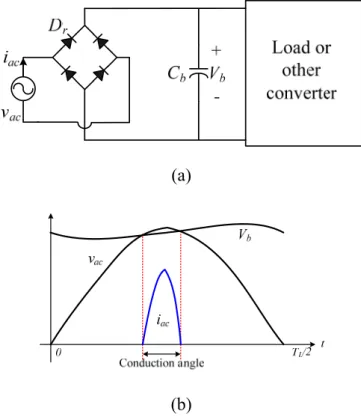
Conventionally, most of the power conversion equipment employs either diode rectifier or thyristor rectifier with a bulk capacitor to converter AC voltage to DC voltage before proc-essing it. For example, Fig. 1.1(a) shows the circuit diagram of a diode-bridge rectifier. The diode bridge Dr rectifies the AC input voltage and the capacitor Vb smoothes out the resulting
voltage to make it an almost pure DC waveform. The current drawn from the AC utility source, however, has a pulse-like non-sinusoidal waveform because the bridge diodes conduct current only when the rectified input voltage is equal to or greater than the bulk capacitor voltage. As a result, the input current waveform has narrow conduction angle and strong dis-tortion, as shown in Fig. 1.1(b).
For any electrical equipment drawing power from the utility, power factor (PF) is a widely used term to evaluate the quality of input power accomplished. Obviously, the di-ode-bridge rectifier shown in Fig. 1 has a poor PF because of the non-sinusoidal input current. This current has a pulsating shape and thus contains large harmonic components that are in-jected into the utility supply. If vast numbers of such converters are used in industry, the har-monics injected in the utility will be so large that they will create a need for increasing volt-ampere ratings of utility equipment (i.e., transformers, transmission lines, and generators) and distort the utility voltage.
(a)
(b)
Fig. 1.1 Conventional diode-bridge rectifier: (a) circuit diagram and (b) key waveforms in a half line cycle.
Since a severely distorted AC utility voltage can damage sensitive electrical equipment, regulatory agencies around the world have established standards on the current harmonic content produced by electrical equipment [1]-[4]. Stricter regulatory agency standards on harmonic content have resulted in the demise in popularity of the simple diode-bridge rectifier as the front-end converter in electrical equipment. Meanwhile, more and more electrical equipment manufacturers are forced to improve or correct the input PF of products supplied by an AC utility source. To comply with the line harmonics standards, a variety of passive and active power factor correction (PFC) techniques have been proposed [5], [6]. The passive techniques normally use a simple line-frequency LC filter to both extend the current conduc-tion angle and reduce the total harmonic distorconduc-tion (THD) of the input current of the di-ode-bridge rectifier. Due to its simplicity, the passive LC filter could be the high efficiency and low cost PFC solution to meet the line current harmonics specifications in the low power
range [7]. However, the passive LC filter has a major drawback which is its heavy and bulky low-frequency filter inductor.
To reduce overall size and weight and increase the power quality further, the active PFC techniques have been introduced. In an active PFC converter, the filter inductor is operated at the switching frequency, which is normally in the 10 kHz to hundreds of kHz range. There-fore, the size and weight of the power converter can be significantly reduced by using a high-frequency inductor. The cost of the active PFC approach can also be lower than that of the passive filter approach if the conversion power increases. In general, the single-phase ac-tive PFC techniques can be divided into two categories: the two-stage approach and the sin-gle-stage approach [8], [9]. These two approaches are introduced in the following.
1.1.1 Two-Stage AC-DC Conversion Technique
The most popular implementation of active PFC is two-stage approach. In this method, an active PFC stage is adopted as the front-end to force the line current to track the line age, therefore achieving unity input PF. The PFC front-end stage converts the AC input volt-age into DC voltvolt-age on a bulky energy-storvolt-age capacitor. Then a conventional DC-DC con-verter is used as the second stage to provide isolation and regulated output voltage.
Figure 1.2 shows an example circuit of the two-stage AC-DC converter. The first PFC stage can be a boost, buck-boost or flyback converter. Generally, the boost converter is the most popular topology. In the PFC stage, there is an independent PFC controller, which con-trols the PFC switch S1 in order to achieve sinusoidal input current waveform [10].
Mean-while, the PFC front-end stage also provides a loosely regulated high DC bus voltage Vb with
small double line-frequency ripples. In general, Vb is loosely regulated around 380–400 V,
even the line input voltage changes from 90 to 260 Vrms for the universal-line applications.
pro-vides a tightly regulated low output voltage Vo with a high bandwidth feedback control loop.
Fig. 1.2 Example circuit of the two-stage AC-DC converter.
The boost inductor in the PFC stage can be operated in several different conduction modes, such as discontinuous conduction mode (DCM), variable-frequency critical (boundary) conduction mode, and continuous conduction mode (CCM). In terms of control implementa-tion, the DCM PFC approach requires the simplest control. The PFC switch S1 is operated
with a constant duty ratio and fixed switching frequency during a half line cycle, without sensing the input voltage or current [11], [12]. This provides a low cost solution for low power applications. The drawback of the DCM boost rectifier is its high input inductor cur-rent ripple, which causes high curcur-rent stress on the semiconductor switch and requires a large electromagnetic-interference (EMI) filter. To reduce the input current ripple, the critical mode PFC provides an alternative solution with a slightly more complicated control circuit, for in-put power of up to 500–600 W. In the critical mode PFC, the boost switch is operated with a variable switching frequency in a half line cycle [13], which keeps the boost inductor operat-ing at the boundary of DCM and CCM. The boost inductor current ripple has a peak value of twice that of the average input current. The variable frequency control also spreads the noise spectrum in the wide frequency range, which can further reduce the EMI filter size [14].
How-ever, the wide switching frequency range causes difficulty in the optimal design of filter. Be-sides, the input current ripple is still large. To further reduce the current ripple and EMI filter size, the CCM PFC approach is widely adopted in the power range from hundreds of watts to several kilowatts. The CCM PFC performs very well, but it requires the most complicated control implementation [10].
In summary, the active two-stage PFC converter has good input PF and can be used in wide ranges of input voltage and output power. This technique is mature and the converter has good performance. However, it requires additional PFC power stage and PFC controller, so the component count, the circuit size and weight, and the total cost are increased.
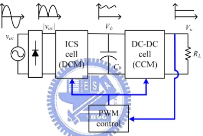
1.1.2 Single-Stage AC-DC Conversion Technique
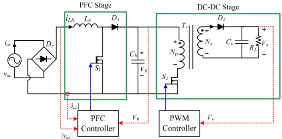
For low power applications, such as computer electronic products, the development trend is to rigorously pursue the reduction of size, weight, and cost. Thus, to reduce the added com-ponent count and cost of the PFC stage in the two-stage approach, cost-effective alternatives attempt to integrate the active PFC input stage with the isolated DC-DC converter. A number of single-stage PFC techniques have been proposed in recent years [15]-[41]. The main objec-tive of this method is really input current shaping (ICS); thus, these circuits are also named as single-stage ICS (S2ICS) converters.
In the S2ICS converter, the PFC inductor is still necessary, but neither the PFC switch nor its controller is needed. The remaining controller is the pulse-width-modulation (PWM) controller, which focuses on the tight regulation of the DC output voltage. Meanwhile, the input PFC function can be automatically achieved. Fig. 1.3 shows how to integrate a boost PFC rectifier with a flyback DC-DC converter to obtain a S2ICS AC-DC converter. When the DC-DC converter is operated in the steady state, the duty ratio of the PWM switch is almost constant during a half line cycle. Moreover, the line current can automatically track the line
voltage by operating the boost inductor in DCM and constant duty ratio, as mentioned in sub-section 1.1.1. This design concept is namely the voltage-follower PFC technique [11] or the self-PFC property [12]. Since the DCM boost switch S1 and the DC-DC converter switch S2
are both operated with constant duty ratio, these two switches can be integrated into one switch by using the same duty ratio and switching frequency [15]. Thus, it is possible to inte-grate a DCM boost PFC rectifier with a flyback DC-DC converter to get a S2ICS AC-DC con-verter without the PFC switch and its controller.
Cb S2 D2 Co RL iLb Vb Vo Np Ns vac Tr Dr iac Lb D1 PFC Stage S1 PWM Controller PFC Controller Vo Vb DC-DC Stage S D3 Co RL Vo Np Ns Tr PWM Controller Vo Cb Vb iLb Lb D2 S2ICS Converter vac Dr iac D1 DC-DC cell ICS cell
Fig. 1.3 Combining a DCM boost PFC front-end and a PWM DC-DC converter to obtain a S2ICS AC-DC converter.
harmonics are small enough to meet the current harmonic constraints, such as the IEC 61000-3-2 Class D. Since instantaneous AC input power always varies, an internal bulk ca-pacitor Cb is needed to buffer the instantaneous difference between the varying input power
and a constant output power such that the output voltage is regulated tightly and free of line frequency ripple. Unlike in the two-stage PFC converter, the bulk capacitor voltage Vb in the
S2ICS converter is no longer regulated and varies with the line voltage and load current since the control freedoms are reduced by integrating the PFC and DC-DC switches into one switch.
Moreover, the design of control circuit and power stage of the DC-DC cell is the same as that of a conventional switching-mode power supply. For the DC–DC regulator circuit, work-ing in the CCM is usually the preferred mode of operation, due to the lower turn-off loss and smaller current stress on the semiconductor devices. Therefore, the combination of a DCM ICS cell and a CCM DC-DC cell is deemed to be ideal for S2ICS converters. A general block diagram of S2ICS converters is shown in Fig. 1.4. However, this approach has an undesirable feature: high bulk capacitor voltage stress at light load. It should be noted that this issue may become severe and critical while the situation with high line and light load occurs [33]. To ex-plain why the bulk capacitor voltage arises while the load becomes light, Fig. 1.5 is given as follows. This figure shows the relationship between the average input power over a half line cycle Pin(ave) and the duty ratio in the ICS cell, and between the average output power over a
half line cycle Po(ave) and the duty ratio in the DC-DC cell.
Assume that the original value of the average input power and average output power is
P1. Since the DC-DC cell operates in CCM, the duty ratio will not change when the output
power suddenly drops from P1 to P2. As shown by the solid curves of Fig. 1.5, it can be seen
that the input power still stays in the original power P1 due to the unchanged duty ratio D1.
Since P1 is greater than P2, the fact that the excess input energy will be stored in the bulk
curves. Under constant output voltage control, the duty ratio will decrease from D1 to D2.
Fi-nally, new balance arrives, where Pin(ave) = Po(ave) = P2 and Vb = Vb2 > Vb1. Consequently, the
power balance at light load is reached at the penalty of significant bulk capacitor voltage stress. In the high line and light load condition for universal line applications, the generated bulk capacitor voltage could be as high as over 1000 V such that selection of switches and capacitors is limited and very costly [33], [49]. Thus, this drawback makes the single-stage designs impractical for the applications that require a universal input voltage of 90–260 Vrms and a wide range of load variation.
Fig. 1.4 Functional block diagram of a typical single-stage AC-DC converter.
Po(ave) Pin(ave) D D ICS cell DC-DC cell CCM CCM DCM DCM Vb1 Vb2 Vb1< Vb2 D1 D2 P1 P1 P2
1.1.3 Standards Regulating Line Current Harmonics
In the international society, some standards for the harmonic content of the line current of a power converter are published. As early as 1982, the International Electrotechnical Committee (IEC) published its standard IEC 555-2 [1], which was also adopted in 1987 as European standard EN 60555-2, by the European Committee for Electrotechnical Standardi-zation (CENELEC). In 1995, standard IEC 555-2 has been replaced by standard IEC 1000-3-2 [2], and also adopted by CENELEC as European standard EN 61000-3-2.
Standard IEC 1000-3-2 applies to equipment with a rated current up to and including 16 Arms per phase which is to be connected to 50 Hz or 60 Hz, 220–240 Vrms single-phase, or 380–415 Vrms three-phase mains. The standard has been revised several times and a second edition was published in 2000 [3] with an amendment in 2001 [4]. Meanwhile, the standard was renamed as IEC 61000-3-2, which has become the most important and popular standard regulating line current harmonics. It should be noted that the limits do not apply for equip-ment with rated powers of 75W or less (it may be reduced to 50W in the future), other than lighting equipment.
The standard divides electrical equipment into four classes: A, B, C and D. The four classes include electrical equipment as follows:
Class A: Balanced three-phase equipment, household appliances (excluding equipment identified as class D), tools (excluding portable tools), dimmers for incandescent lamps and audio equipment. Equipment not specified in one of the other three classes should be consid-ered as Class A equipment.
Class B: portable tools and arc welding equipment which is not professional equipment. Class C: lighting equipment, including dimming device.
(active input power equal or less than 600 W).
The converters proposed in this dissertation shall be applied in modern electronic prod-ucts, such as personal computers, computer peripherals, and television receivers. All these electronic products’ input power is less than 600W. Therefore, the experimental results will be criticized by employing the standard Class D. The current harmonics limits for Class D are shown in Table 1.1.
Table 1.1 Limits for Class D equipment in standard IEC 61000-3-2 Harmonic wave
Order n
Maximum permissible har-monic current per watt (mA/W)
Maximum permissible har-monic current (A)
3 3.4 2.30 5 1.9 1.14 7 1.0 0.77 9 0.5 0.40 11 0.35 0.33 13 0.21 15 n 39≦ ≦ 3.85/n 0.15×(15/n)
1.2 Motivation and Objectives
Theoretically, changing the two-stage scheme to single-stage scheme can substantially mitigate the cost and complexity of PFC AC-DC converter. However, the concept of sin-gle-stage design still has not been extensively adopted in today’s power products. This is be-cause there are still some of the existing technical challenges with respect to the development of viable S2ICS AC-DC converters, such as high voltage stress, high current stress and low conversion efficiency, etc.
With the enforcement of newly issued international regulations, the cost-effective sin-gle-stage AC-DC conversion has become one of the hottest research areas in power electron-ics. This dissertation is intended to address the major technical issues in existing single-stage
1.3 Dissertation Outline
This dissertation is composed of five chapters. The content of each chapter is briefly de-scribed as follows:
Chapter 1 introduces the background regarding the present power factor correction tech-niques and line current harmonics standard. It then lists the research motivations and objec-tives.
Chapter 2 offers a review for proposed techniques for the single-stage AC-DC converters and discusses various issues, trend and challenges.
Chapter 3 first introduces the mechanism of the proposed ICS technique. Then, a new flyback converter employing the proposed ICS scheme is presented. The content in this chap-ter contains circuit description, operation principle, circuit design procedure, and prototype experiment results. In addition, an extended circuit based on topology refinement is proposed for specific applications.
Chapter 4 deals with the problem regarding high bulk capacitor voltage stress at light load. A new flyback-forward converter with the modified ICS scheme proposed in Chapter 3 is presented. The mechanism and performance of the proposed approach for suppressing bulk capacitor voltage stress are discussed in detail. The content also covers several segments which are the same as in Chapter 3.
Chapter 5 summarizes the conclusions of this work and presents suggestions for further work in related research directions.
CHAPTER 2
REVIEW OF EXISTING SINGLE-STAGE AC-DC
CONVERTERS
In the last decade, the heat wave of studying single-stage ICS AC-DC converters has re-sulted in hundreds of published papers. For single-stage AC-DC converters, the performance measures, such as efficiency, component count and circuit complexity, component voltage and current stresses, input current quality, etc., are largely dependent on the circuit topology. Thus, the main objective of this chapter is to present a topological study of the representative S2ICS converters and find a topological relationship among various converters. This study can be used to topologically explain the main drawbacks of current S2ICS converters and pursue po-tential topology variations to overcome the barriers that limit the application of S2ICS con-verters.
2.1 Familiar Single-Stage Input Current Shaping (S
2ICS) Converters
The concept for S2ICS AC-DC converters can be traced back to some early work pre-sented in 1991 [18], [19]. In article [18], Kherulawa et al. proposed a single power stage with dual outputs, including the desired DC output and a boosting supply in series with the input, as shown in Fig. 2.1. Without active control of the boost supply, a reasonably good input cur-rent shape can be obtained due to the natural characteristics of the boost resonant circuit. This circuit is original but the component count is high. Takahashi et al. proposed another way to realize S2ICS AC-DC converters, which cascades a boost ICS circuit with a DC-DC converter using one switch [19]. As shown in Fig. 2.2(a), a high frequency “dither source” is inserted between the input boost inductor L and the bulk energy-storage capacitor C . Since the dither
source introduces high-frequency pulsating voltage on Lb during one line cycle, the rectifier
diode can conduct current even while the instantaneous input line voltage is much lower than the capacitor voltage Vb, as shown in Fig. 2.2(b). As a result, the input current conduction
an-gle is significantly enlarged and the input current harmonics are reduced. This circuit presents an early form of the single-stage PFC method that integrates a boost PFC rectifier with a DC-DC converter in a cascade fashion.
So far, many papers have been presented about integrated single-stage AC-DC conver-sion techniques. In order to systematically understand the basic structure and specific per-formance of various converters, it is necessary to categorize the representative circuits pub-lished in recent years. Our survey will focus on the single-stage designs with boost-type ICS cells. From several points of view, including power flow paths, topology structures, and input current shapes, these circuits can be divided into the following categories as introduced in subsections 2.1.1–2.1.4.
(a)
(b)
Fig. 2.2 General structure of “dither-rectifier” and its waveforms [19]: (a) Circuit diagram, (b) conceptual waveforms.
2.1.1 S2ICS Converters with Cascade or Parallel Power Processing Structure
Conventional single-stage AC-DC converters were derived from two-stage scheme and thus synthesized with a cascade method [15]. As shown in Fig. 2.3(a), the single-stage AC-DC converters have the dominant configuration integrating two circuit parts. The first
is a DC-DC circuit with a bulk capacitor Cb placed between this circuit and the ICS cell. The
downstream DC-DC cell is used to realize fine output regulation, isolation, and fast dynamic response. In terms of power transfer, the AC input power in such a design must first be trans-ferred into the intermediate bulk capacitor Cb; this process is completed by the ICS cell. Then
the power stored on the bulk capacitor Cb is processed again by the DC-DC cell to reach final
output. The block diagram for explaining power transfer is shown in Fig. 2.3(b). This double power processing results in low conversion efficiency, which is the product of the efficiency of each functional cell.
(a)
(b)
Fig. 2.3 S2ICS converter with cascade power processing structure: (a) example circuit [15] and (b) power transfer block diagram.
In order to improve conversion efficiency, some new power transfer approaches have been proposed in [22]–[28] which allow a part of the input power to be processed only once and let the remaining input power to be processed twice while still achieving both high PF and tight output regulation. Those power transfer approaches provide a new way to achieve more efficient and higher power rating S2ICS converters than the conventional double power
processing approach shown in Fig. 2.3. An example circuit of the direct power transfer ap-proach is shown in Fig. 2.4(a) and its power transfer block diagram is shown in Fig. 2.4(b).
(a)
(b)
Fig. 2.4 S2ICS converter with parallel power processing structure: (a) example circuit [25] and (b) power transfer block diagram.
2.1.2 S2ICS Converters with Two-Terminal or Three-Terminal ICS Cells
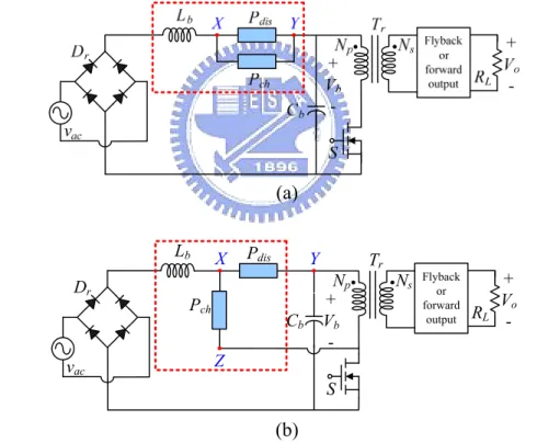
With the consideration of ICS realization mechanism, the ICS circuits can be symbolized as two- or three-terminal cells [16], [17]. Each ICS cell contains a boost inductor Lb and two
branches, as shown in the dotted rectangle in Fig. 2.5. The charging path Pch is used to charge
the boost inductor when the switch S is on. The discharging path Pdis is used to discharge the
boost inductor and transfer the energy from the boost inductor to bulk capacitor or output when the switch S is off. The two paths are usually composed of diodes, capacitors, inductors, and extra windings of the transformer or their combinations.
Lb are connected in parallel and inserted between the full-bridge rectifier Dr and the bulk
ca-pacitor Cb, as shown in Fig. 2.5(a). Notice that one winding coupled to the transformer of a
DC-DC converter is contained in the charging path. The polarity arrangement of the addi-tional winding intends the voltage across it being in opposition to the bulk capacitor voltage
Vb during the duty-on time of switch S. Therefore, when the switch is on, the voltage across
the winding can cancel the capacitor voltage Vb, so that the charging voltage of the boost
in-ductor only includes the input voltage. The well-known magnetic-switch (MS) topology pro-posed in [20] is an example circuit, as shown in Fig. 2.6(a). In this converter, the charging and discharging paths use the same branch, namely, MS winding. Contrarily, in the example cir-cuit shown in Fig. 2.6(b), the charging and discharging paths use the different branches [29].
(a) Tr RL + Vo -S Lb vac Pch Np Ns Dr Cb + Vb -X Flyback or forward output Pdis Y Z (b)
Fig. 2.5 Single-stage AC-DC converters with ICS cell of (a) two-terminal and (b) three-terminal.
(a)
(b)
Fig. 2.6 Example circuits of S2ICS converter with two-terminal ICS cell: (a) the charging and discharging paths use the same branch [20] and (b) the charging and discharging paths use the different branches [29].
In the implementation of the three-terminal ICS cell, the boost inductor Lb is connected
to the full-bridge rectifier Dr; the discharging path is connected to the bulk capacitor Cb; and
the charging path is connected to switch S, as shown in Fig. 2.5(b). Therefore, the circuit con-figuration is named three-terminal. Similar to the two-terminal ICS cell, the boost inductor is charged by the input voltage when the switch is on, and discharged through the discharging path. The converter shown in Fig. 2.3(a) is an example circuit.
It is found that the two S2ICS families are functionally equivalent and exhibit very simi-lar performance although they are topologically different [16], [17]. For example, the con-verter shown in Fig. 2.6(b) is functionally equivalent to the one shown in Fig. 2.3(a) when the turns ratio of winding N1 is the same as that of winding Np.
2.1.3 S2ICS Converters with DCM or CCM ICS Cells
In most of the existing S2ICS converters, the ICS cells are operated in DCM to auto-matically achieve input PFC function. The mechanism is explained as follows. Since instan-taneous AC input power always varies, a bulky capacitor is needed to buffer the instaninstan-taneous difference between the varying input power and a constant output power such that the output voltage is regulated tightly and free of line frequency ripple. Because the bulk capacitor is sufficiently large, the bulk capacitor voltage Vb can keep in the condition with small ripple.
Thus, the switch duty cycle is almost constant during one line cycle in the steady-state, and the line current can automatically track the line voltage by operating the boost inductor in DCM, as shown in Fig. 2.7(a).
Although the concept of the basic DCM S2ICS is very simple, it will introduce higher input inductor current ripple and more power loss due to the relatively high current stress. To reduce EMI filter size and improve conversion efficiency, several new CCM ICS techniques have been proposed in resent years [36]-[41]. Most of these methods are implemented by in-creasing the boost inductance or adding extra passive components to the DCM ICS cell. The corresponding input current waveforms are shown in Fig. 2.7(b). Although the line current generated by the CCM ICS cell is slightly deformed as compared to sinusoid, it has low har-monic components and can meet IEC 61000-3-2 Class D requirements.
i
Lb|i
ac|
t
(a) (b) Fig. 2.7 Boost inductor current and its corresponding line current waveforms generated by
2.1.4 S2ICS Converters with Current-Source or Voltage-Source ICS Cells
To achieve CCM boost inductor current, several CCM S2ICS techniques have already been proposed in recent years [38]-[41]. Among them, there are two typical CCM S2ICS techniques. Fig. 2.8 shows one type of CCM S2ICS technique that incorporates an additional high-frequency inductor L1. Fig. 2.9 shows another CCM S2ICS technique with an additional
high-frequency capacitor C1. Since the inductor L1 is comparable to a high-frequency current
source, the circuits in Fig. 2.8 are named as current-source S2ICS (CS-S2ICS) converters. Similarly, since the capacitor C1 is comparable to a high-frequency voltage source, the circuits
in Fig. 2.9 are named as the voltage-source S2ICS (VS-S2ICS) converters. As shown in Figs. 2.8 and 2.9, each circuit utilizes an additional passive component, L1 or C1, on the original
DCM S2ICS to get continuous inductor current.
Tr RL + Vo -S Lb vac Np Ns Dr Cb + Vb -Flyback or forward output D1 D2 L1 N1 Tr RL + Vo -S Lb vac Np Ns Dr Cb + Vb -Flyback or forward output D1 D2 L1 (a) (b) Fig. 2.8 Current-source S2ICS Converters with ICS cell of (a) two-terminal and (b)
three-terminal. Tr RL + Vo -S Lb vac Np Ns Dr Cb + Vb -Flyback or forward output D1 D2 C1 N1 Tr RL + Vo -S Lb vac Np Ns Dr Cb + Vb -Flyback or forward output D1 D2 C1 (a) (b) Fig. 2.9 Voltage-source S2ICS Converters with ICS cell of (a) two-terminal and (b)
2.2 Main Issues of Single-Stage AC-DC Scheme
The underlining strategy of the single-stage AC-DC scheme is to design the converter that allows its PFC and DC-DC conversion circuits to share the same power switch with the same controller. From the above existing research efforts, we found that this kind of arrange-ment results in several main issues.
The first issue is the high current stress on the power switch since it handles current from both the AC mains and the bulk capacitor synchronously. Moreover, the ICS cell in a S2ICS AC-DC converter normally operates in DCM to utilize its inherent current shaping capability; therefore, this issue becomes more deteriorated. Obviously, when compared with the conven-tional two-stage schemes, S2ICS AC-DC converters have relatively high switch current stress. High current stress not only causes low conversion efficiency and high temperature rise, but also brings about annoying EMI issues.
The second issue is that the bulk capacitor voltage stress is critical since it is no longer regulated and increases while the input line voltage increases or load current decreases. This is because only a single control loop for the output voltage regulation, and the bulk capacitor voltage is determined by the input to output average power balance [33]. The high bulk ca-pacitor voltage stress generally exists for most of S2ICS converters, and this issue is more se-vere under high line and light load condition [49]. Thus, it is difficult to use S2ICS converters for the applications that require a universal input voltage of 90–260 Vrms. Moreover, a high bulk capacitor voltage means high component rating, high cost and low conversion efficiency. For the commercial consideration, the maximum bulk capacitor voltage must be held below 450 V, so that a commercially available 450 V-rated electrolytic capacitor can be used safely.
2.3 Several Familiar Schemes to Alleviate Bulk Capacitor Voltage Stress
Many off-line power supplies must be able to have a universal-line input, which meansthe power converter may be operated with the international utility voltage. For example, in the United States, the single-phase input voltage is in the 90–135 Vrms range, while the input voltage is in the 180–260 Vrms range in Europe. A wide line voltage range may pose an enormous challenge to designing S2ICS converters, especially in alleviating bulk capacitor voltage stress. To suppress high bulk capacitor voltage stress, numerous methods have been presented [50]. In this section, four representative schemes to suppress bus capacitor voltage stress are analyzed and discussed. Through understanding the approaches of alleviating bus capacitor voltage stress, it is helpful to derive and develop new topologies of S2ICS convert-ers.
2.3.1 Variable-Frequency Control
The variable-frequency control was proposed in [49]. Since the voltage gain of the CCM DC-DC cell depends only on the duty ratio, and the voltage gain of the DCM boost-type ICS cell depends on the switching frequency rather than the duty ratio, it is possible to regulate the bulk capacitor voltage by a variable-frequency control. Clearly speaking, for the ICS cell op-erating in DCM with a constant duty ratio, the average input power is inversely proportional to the switching frequency, and the unbalanced power between the input and output decreases with the increase of switching frequency. The drawback of this approach is that large load variation range results in large range of variation in switching frequency. For a load change from 10% to full load, the switching frequency has to be 10 times that of the full load to re-main the same bulk capacitor voltage. Such wide switching frequency variation has problems such as low conversion efficiency and difficulty in the optimal design of transformers and in-ductors.
2.3.2 Bulk Capacitor Voltage Feedback Concept
Fig 2.10 shows the modified BIFRED (Boost Integrated with Flyback Rectifier/Energy Storage/DC-DC converter) converter with the bulk capacitor voltage feedback [33]. In the modified scheme, an additional transformer winding N1 is inserted in series with the boost
inductor. The winding can feedback the bulk capacitor voltage when the boost inductor is charged, and the feedback depth depends on the bulk capacitor voltage level. The feedback depth will increase when the bulk capacitor voltage has an increasing trend. Thus, the input power can be automatically reduced to guarantee the balance between input and output aver-age power. As a result, the bulk capacitor voltaver-age is limited within a proper range.
Fig. 2.10 BIFRED converter with bulk capacitor voltage feedback [33].
2.3.3 Parallel Power Processing
To reduce extra bulk capacitor voltage stress and extra switch current stress, a parallel power factor correction (PPFC) approach has been proposed [22]-[28]. The main advantage of this type of design is the clamped or slightly boosted bulk capacitor voltage since partial input power is processed only once and directly delivered to the output load rather than stored in Cb.
The configuration shown in Fig. 2.11 is an example circuit [24], in which the additional fly-back transformer Tr1 is used to replace most functions of the boost inductor in a conventional
S2ICS AC-DC scheme and provide a path for direct power transfer. This scheme can be ap-plicable to converters with wide input voltage and load ranges. However, the two transformers (Tr1 and Tr2) with similar size and complex circuit structure make this topology less attractive
in low power applications, for which cost and size are often the dominant concerns.
Fig. 2.11 Example circuit with parallel power processing [24].
2.3.4 Both Functional Blocks Operate in the Same Mode
As discussed in subsection 1.1.2, power imbalance between the input and the output in the operation combination of DCM ICS + CCM DC-DC will cause high voltage stress on the intermediate bulk capacitor. However, there is no high bulk capacitor voltage stress problem in the combinations with the same operating mode, either in DCM or in CCM for the two cells [33]. Taking the example of DCM ICS + DCM DC-DC, the duty ratio will automatically decrease while the load becomes light, as shown in Fig. 2.12. As a result, the average input power also decreases due to the decrease of duty ratio. The excess input energy reduces ac-cordingly and the bulk capacitor voltage can be suppressed [51].
The technique of operating both functional blocks in the same mode is a practical and useful solution. However, the combination of DCM ICS + DCM DC-DC causes a low effi-ciency because of higher conduction loss and turn-off switching loss; the combination of CCM ICS + CCM DC-DC has relatively lower PF and higher distortion in input current as well as the larger boost inductor.
Fig. 2.12 Relationship between the average input power, average output power, and duty ratio for DCM ICS + DCM DC-DC [33].
2.4 Trend and Challenges
For AC-DC conversion, although unity PF is the ideal objective, it is not necessary to meet today’s regulations with unity PF. For example, both IEC 555 and IEC 61000-3-2 allow the presence of harmonics in the line current [1]-[4]. This fact opens the door for the com-promise techniques between quality and cost, which are capable of overcoming the above is-sues. Thus, to sum up briefly, the design optimization of a S2ICS circuit needs to meet the following objectives:
(1) The input current harmonics must meet the IEC 61000-3-2 Class D specifications; (2) The S2ICS converter should have low bulk capacitor voltage stress in order to
mini-mize the component ratings;
(3) The circuit structure should be simple to maintain lower cost for this converter than it is with the two-stage approach;
(4) The converter should have low switch current stress and good efficiency as well as keep Vb below 450 V in a wide line voltage range.
har-monic specifications, limiting bulk capacitor voltage stress, reducing switch current stress, dealing with the universal-line input voltage range, all with minimum additional cost. How to understand, analyze, optimize and improve these S2ICS converters has been a very interesting topic in recent power electronics research.
2.5 Concluding Remarks
A review of existing S2ICS AC-DC converters is given in this chapter. For further com-paring the system configuration and characteristics of the familiar S2ICS converters, we summarize the classification of the representative reported single-stage circuits as shown in Table 2.1.
In addition, main issues such as high current stress, high voltage stress and low conver-sion efficiency in current S2ICS AC-DC approaches are also presented and discussed in this chapter. To alleviate switch current stress, a new ICS technique is presented in Chapter 3. The proposed ICS scheme not only alleviates switch current stress in the duty-on time, but also provides a well current shaping function. Moreover, to suppress bulk capacitor voltage stress, a hybrid operated DC-DC converter is adopted in Chapter 4. This circuit can simultaneously achieve two functions including bulk capacitor voltage suppression while light load and high conversion efficiency while heavy load.
Table 2.1 Classification of the representative reported S2ICS converters Basis of classification Category Representative Circuits
Cascade [15], [31], [32] Power processing structure
Parallel [22]-[28] 2-terminal [20], [29], [30] Topology configuration of ICS cell 3-terminal [21], [23]-[28], [31]-[41] DCM [15], [21]-[23], [25]-[35], [51] Input boost inductor current
waveform
CCM [24], [36]-[41]
CS-S2ICS [36]-[39] Topology configuration of
CHAPTER 3
ANALYSIS OF THE PROPOSED ICS TECHNIQUE AND THE
APPLICAION TO FLYBACK CONVERTERS
For the single-stage designs with boost-type ICS cells, the line current actually being the average (or filtered) boost inductor current is composed of two components. The average charging current of the boost inductor has linear relation to the instantaneous line voltage, while the average discharging current of the boost inductor primarily has a quadratic charac-teristic against the instantaneous line voltage. Thus, the resultant input i-v characcharac-teristic curves are nonlinear as shown in Fig. 3.1(a) and the corresponding line currents have the de-formed shapes as shown in Fig. 3.1(b), where M represents the ratio of the bulk capacitor volt-age Vb to the peak line voltage Vac(pk). To improve this drawback, it is found that Vb should be
designed to be as high as possible [11]. However, this will produce high voltage stress on the switch and the bulk capacitor. To remedy the problems described above, the charging time of the boost inductor in the proposed converter is designed to be inversely modulated by the line voltage, so that the i-v curve of the average charging current presents an opposite deformation characteristic to that presented by the i-v curve of the average discharging current. Conse-quently, the line current has the waveform analogous to the line voltage waveform.
In addition, since the ICS cell and DC-DC cell are driven by one common switch, both the boost inductor current and the transformer current simultaneously flow through the switch in the duty-on time, as shown in Fig. 3.2(b). As a result, the switch current stress is relatively high when compared with the conventional two-stage scheme. High current stress not only accompanies with increased power loss, but also brings about annoying EMI issues. To over-come this drawback, we adopt the concept of “interleaved operation” in the design of
sin-gle-stage AC-DC converters. Unlike the conventional sinsin-gle-stage designs, the proposed ICS scheme is intentionally arranged to be charged in the duty-off time, as shown in Fig. 3.2(c). With this design, the switch current stress in the duty-on time can be significantly reduced and correspondingly conduction loss can be relieved. This special ICS function can be imple-mented by using the technique of multi-winding of power transformer.
0 0.2 0.4 0.6 0.8 1 0 0.1 0.2 0.3 0.4 0.5 0.6 0.7 0.8 0.9 1 N or m al iz ed l ine cur rent am pl it ude
Normalized line voltage amplitude
0 0.5 1 1.5 2 2.5 3 0 0.1 0.2 0.3 0.4 0.5 0.6 0.7 0.8 0.9 1 N or m al iz ed l ine cur rent am pl it ude
Line angle (rad)
(a) (b) Fig. 3.1 The line current distortion caused by the modulation effect of the boost inductor
discharging time, where M = Vb/Vac(pk) and the dead angle of the line current is considered: (a)
the input i-v characteristic curves and (b) the corresponding line current waveforms.
On the other hand, the common drawback of using the single-stage circuits is that the switching components often suffer from the relatively high voltage and current stress during switching, which increases the component rating and introduces more switching loss too. To further improve the performance of the proposed single-stage AC-DC converter, an ac-tive-clamp circuit with zero-voltage-switching (ZVS) function is added to the adopted con-verter. This circuit can lead to noticeable improvement on voltage spikes across the switches and significant reduction of electromagnetic noise generation [42]-[48].
Fig. 3.2 Comparison of switch current stress: (a) PWM control signal of the switch, (b) switching current waveforms of the conventional ICS scheme and (c) switching current wave-forms of the proposed ICS scheme.
3.1 Analysis of the Proposed Converter
3.1.1 Circuit Derivation and Configuration
Fig. 3.3 shows the circuit configuration of the proposed single-stage AC-DC converter. The proposed converter is based on a conventional active-clamp DC-DC converter with skilled modification in order to satisfy harmonic regulations and cost-effective consideration. In this converter, a multi-winding transformer Tr is employed. It includes three windings N1, N2, and N3 with turns number n1, n2, and n3, respectively, and the primary magnetizing
induc-tance Lm. As shown in Fig. 3.3, the converter contains an ICS cell, mainly composed of the
rectifier diode D1, boost inductor Lb, winding N1, and resonant inductor Lr. The diode D1 is
used to provide fast rectification and prevent the filter capacitor Cin from being charged by the
de-sign in which the undotted end of winding N1 is intentionally connected to node X instead of
node Y. There are two objectives for this design: charging the boost inductor in the duty-off time and reducing the size of the boost inductor. Through the winding N1 with enough large
turns, the voltage vN1 can force to charge Lb during the duty-off time since vN1 turns to
nega-tive. Therefore, only the transformer current flows through the main switch S1 in the duty-on
time and correspondingly the switch current stress can be reduced. Meanwhile, the resonant inductor Lr is arranged in the charging path of Lb so that Lr and Lb can provide the
volt-age-boost function together. Consequently, a small inductance for Lb is sufficient to achieve
the DCM operation and it can be implemented by either an external inductor or leakage in-ductance of the transformer.
The ICS cell is then followed by an active-clamp DC-DC circuit which provides isolation and post-regulation function, as defined by the dotted-line box in Fig. 3.3. The DC-DC cell is designed to operate in CCM and can be implemented by a flyback or forward circuit. Cr
represents the sum of the parasitic capacitances of main switch S1 and auxiliary switch S2. Lr
represents an external inductor, which forms a series resonant circuit with Cr to enable
soft-switching function. The resonant inductor Lr, the clamping capacitor Cc, and the auxiliary
switch S2 form the main part of the active-clamp circuit for limiting the turn-off voltage spike
of S1.
The control circuit can be implemented by a simple control loop, a common PWM con-troller, and a driver circuit. Moreover, main and auxiliary switches are driven complementary with small dead time in between to allow for ZVS.
Fig. 3.3 Proposed single-stage soft-switching AC-DC converter.
3.1.2 Principle of Operation
In this subsection, the detailed operation of a flyback-type implementation with the pro-posed ICS scheme is introduced. To simplify the analysis, the following assumptions are made:
(i) The switching and conduction losses of the components are neglected;
(ii) The rectified line voltage |vac| is considered constant during a switching period;
(iii) The bulk capacitor voltage Vb and the output capacitor voltage Vo are ripple-free DC
in each half of a line cycle;
(iv) The leakage inductances of the transformer are neglected; (v) An external inductor is employed for Lb.
According to the instantaneous magnitude of the rectified line voltage |vac|, the operation
of the converter can be divided into two modes during a half line cycle, as shown in Fig. 3.4. When |vac| is smaller than the boundary voltage VBD, the converter operates in mode M1, and
during the remaining time it operates in mode M2. Fig. 3.5 illustrates that five topological
states exist in a switching period. Referring to the symbol definitions, topological states, and key waveforms shown in Figs. 3.3, 3.5, and 3.6, respectively, the detailed operation is
ex-plained as follows.
Fig. 3.4 Operation modes in a half line cycle.
(a) (b) (c)
(d) (e) (f)
Fig. 3.5 Topological states of the proposed converter based on flyback topology:
(a) State 1, (b) State 2, (c) State 3 for mode M1, (d) State 3 for mode M2, (e) State 4, and (f)
v
GS1v
GS2v
DS1i
N3i
N1i
Lr t0 t1 t2 t3t4 M1 M2 t5 1 State 2 3 4 5i
S1v
DS2v
ci
Lmv
GS1v
GS2v
DS1i
N3i
N1i
Lr 1 State 2 3 4 5i
S1v
DS2v
ci
Lm 1 Ds5Ts DTs DTs Ds5Ts t0 t1 t2 t3t4 t5v
N2v
N2 (a) (b)Fig. 3.6 Steady-state waveforms of the proposed converter in (a) mode M1 and (b) mode M2.
State 1 [Fig. 3.5(a), t0≤t<t1]:
At t0, S1 is on and S2 is off. The output rectifier D2 is reverse biased. Both Lm and Lr are
( )
( )
( )
( )
0(
t t0 L L V t i t i t i t i m r b Lr Lm Lr P = = = + + ⋅ −)
. (3.1)Thus, ip(t1) can be obtained by
( )
( )
(
s s m r b Lr P D D T L L V t i t i 1 0 ⋅ − 5 + + =)
. (3.2)where D is the duty ratio, Ds5Ts = (t5–t4), and Ts is the switching period. In this duration, the
current flowing through Lb is zero.
State 2 [Fig. 3.5(b), t1 ≤t<t2]:
At t1, S1 is turned off. Cr is rapidly charged by the magnetizing current iLm in this duration;
thus, vDS1 rises linearly to reach Vb +vc
( )
t2 in a short time and is given by( )
( ) (
1 1 1 t t C t i t v r P DS = ⋅ −)
. (3.3) State 3 [Fig. 3.5(c) or 3.5(d), t2 ≤t<t3]:At t2, vDS1 rises to the value that makes the body diode of S2 start to conduct. In this
dura-tion, the transformer secondary voltage vN3 is sufficient to forward bias D2. Therefore, the
transformer primary voltage vN2 is clamped at −Vo⋅n2 n3. Shortly, S2 is turned on before ip
resonates to the negative direction; thus, ZVS of S2 is achieved. In mode M1, the line voltage
is not large enough to generate iLb; thus, the resonant tank only includes Lr and Cc when
ne-glecting the small Cr. The voltage and current along the resonant loop can be obtained by

![Fig. 2.1 Isolated S 2 ICS technique using a two-output dual-control converter [18].](https://thumb-ap.123doks.com/thumbv2/9libinfo/8229454.170856/24.892.166.776.470.879/fig-isolated-ics-technique-using-output-control-converter.webp)
![Fig. 2.2 General structure of “dither-rectifier” and its waveforms [19]: (a) Circuit diagram, (b) conceptual waveforms.](https://thumb-ap.123doks.com/thumbv2/9libinfo/8229454.170856/25.892.205.725.117.845/general-structure-rectifier-waveforms-circuit-diagram-conceptual-waveforms.webp)
![Fig. 2.3 S 2 ICS converter with cascade power processing structure: (a) example circuit [15] and (b) power transfer block diagram](https://thumb-ap.123doks.com/thumbv2/9libinfo/8229454.170856/26.892.258.681.436.800/converter-cascade-processing-structure-example-circuit-transfer-diagram.webp)
![Fig. 2.4 S 2 ICS converter with parallel power processing structure: (a) example circuit [25] and (b) power transfer block diagram](https://thumb-ap.123doks.com/thumbv2/9libinfo/8229454.170856/27.892.145.780.201.725/converter-parallel-processing-structure-example-circuit-transfer-diagram.webp)