國 立 交 通 大 學
電子物理學系 電子物理研究所碩士班
碩 士 論 文
完全鎳自我對準矽化源/汲與閘極之薄膜電晶體研究
An Investigation of the Fully Ni-salicided S/D and
Gate in Poly-Si TFTs
研 究 生:王仁杰
指導教授:趙天生 博士
完全鎳自我對準矽化源/汲與閘極之薄膜電晶體研究
An Investigation of the Fully Ni-salicided S/D and
Gate in Poly-Si TFTs
研 究 生:王仁杰 Student:Ren-Jie Wang
指導教授:趙天生 博士 Advisor:Tien-Sheng Chao
國 立 交 通 大 學
電子物理學系 電子物理研究所碩士班
碩 士 論 文
A Thesis
Submitted to Institute of Electrophysics
National Chiao Tung University
In Partial Fulfillment of the Requirements
for the Degree of
Master of Science
In
Electrophysics
June 2005
Hsinchu, Taiwan, Republic of China
完全鎳自我對準矽化源/汲與閘極之薄膜電晶體研究
學生: 王仁杰
指導教授: 趙天生 博士
國 立 交 通 大 學
電子物理學系 電子物理研究所碩士班
摘 要
超薄的絕緣層上矽金氧半場效電晶體的大的源/汲極寄生電阻會使得元件性 能變差。相同的問題也會發生在多晶矽薄膜電晶體。超薄的多晶矽薄膜電晶體限 制了元件的驅動電流。為了減少多晶矽薄膜電晶體的寄生電阻,我們採用完全鎳 自我對準矽化反應去解決這個問題。最近,關於矽化鎳的研究被廣泛地探討。片 電阻方面,矽化鎳(NiSi)的片電阻是跟二矽化鈦(TiSi2)和二矽化鈷(CoSi2)差不多 的。而且鎳金屬矽化物可以在低溫(400~600℃)時形成,而不會有結塊效應 (agglomeration effect)。在矽化鎳的形成過程當中,它消耗較少的矽,所以它可以 形成較淺的接面。 在本論文中,完全鎳自我對準矽化源/汲與閘極多晶矽薄膜電晶體(FSA-TFTs)已經被成功地製造出來。和傳統的多晶矽薄膜電晶體比較的話,完全鎳自我對準
矽化多晶矽薄膜電晶體有較小的源/汲極與閘極片電阻,而且它可以有效地抑制
浮接基體效應(floating body effect)和寄生雙極性接面電晶體效應(parasitic bipolar
junction transistor action)。實驗結果顯示完全鎳自我對準矽化多晶矽薄膜電晶體
有較低的漏電流、較好的次臨界特性、較少的臨界電壓變化量和較大的場效遷移
率。所以完全鎳自我對準矽化多晶矽薄膜電晶體的特性適合用在需要穩定的臨界
An Investigation of the Fully Ni-salicide S/D and Gate in
Poly-Si TFTs
Student: Ren-Jie Wang
Advisor: Dr. Tien-Sheng Chao
Department of Electrophysics,
National Chiao Tung University
ABSTRACT
Large source/drain parasitic resistance degrades device performance in the
ultrathin-film silicon on insulator metal oxide field effect transistors (SOI MOSFETs).
Similar problem also happens in the poly-Si TFT. Large parasitic resistance results in
the limitation of the ON current in the thin-channel poly-Si TFTs. To decrease the
parasitic resistance of the poly-Si TFTs, the fully Ni-salicidation is a technology to
solve this problem. Recently, many researches have been studied about NiSi. The
sheet resistivity of NiSi is comparable with that of TiSi2 and CoSi2. And Ni-
silicidation can be accomplished at low temperature (400~600℃) without
agglomeration effect. During the formation of NiSi, it is the less silicon consumption.
So it can form shallower junction.
In this thesis, a fully Ni self-aligned silicided (fully Ni-salicided) source/drain
on 40-nm-thick channel layer. The FSA-TFTs exhibit small S/D and gate sheet
resistance and can effectively suppress the floating-body effect and parasitic bipolar
junction transistor action, compared to control TFTs. Experimental results show that
the FSA-TFTs give lower off-state leakage, improved subthreshold characteristics,
less threshold voltage variation, and larger field-effect mobility compared with control
TFTs. The characteristics of the FSA-TFTs are suitable for high performance driving
誌謝
兩年充實的光陰,以此論文為長久的求學生涯劃上短暫的句號。在研究的生 涯裡受過很多人的幫忙,在此表達感激之意。首先要感謝指導教授 趙天生老師 在各個方面的指導。老師無論在實驗、論文研討、做人處事上都給予我相當大的 啟發。 再來要感謝在這兩年中不停地指導我的郭柏儀學長。學長嚴謹、認真、不畏 失敗的研究精神,的確是我學習的最佳典範。在研究討論的過程當中,學長不厭 其煩地教導也都使我獲益良多。在此還要特別感謝王獻德學長、羅文政學長、李 耀仁學長、陳建豪學長、謝明山學長、吳偉成學長在實驗及論文上提供我相當寶 貴的意見,也謝謝同期的任逸、志仰、浩偉、賢達、銘福、嘉豪、祥梅、雅欣、 宏穆、健旭、慶潭、陪我一同度過這兩年的光陰。在做實驗的日子裡,和任逸、 志仰互相討論實驗、論文的時光,更是讓我覺得追求學問是一件有趣的事情。實 驗室歡樂的氣氛著實讓我的研究生涯更加的充實。我永遠不會忘記和大家在實驗 室裡面奮鬥的日子。 感謝國家奈米元件實驗室和交通大學奈米中心在儀器設備上的支援,特別感 謝國家奈米元件實驗室的徐台鳳小姐、蔣秋芬小姐、巫振榮先生在製程上的幫 忙,對於諸位口試委員的建議與指證也表感謝之意。 最後,在此我要對我的父親 王元芳先生和母親 林寶蓮女士表達我最深的敬 意。父、母親省吃儉用以讓我有優良的讀書環境,辛苦栽培之情著實讓我留下深 刻的印象。無怨無悔地付出,令我非常地感激。還有非常感謝弟弟和妹妹及女友 慧萍的支持與鼓勵。我在此由衷地謝謝你們,由於你們的關懷、體諒與幫忙,讓 我相信一切辛苦都是值得的,再次感謝。
Contents
Abstract(Chinese) ………I Abstract(English)………III Acknowledge ………...……… V Contents ………..………VI Table Captions ………...………VIII Figure Captions ………..………Ⅸ
Chapter 1 Introduction
1.1 Brief Introduction of Poly-SiTFTs ...………...………...1
1.1.1 Solid Phase Crystallization (SPC) .……….2
1.1.2 Excimer Laser Annealing (ELA)……….2
1.1.3 Metal Induced Crystallization(MIC) ………...…………3
1.2 Introduction of some material for salicide process ……….………...3
1.3 Motivation ……….……….………5
1.4 Organization of the Thesis………..…………..………..5
Chapter 2
Experimental process
and Electrical parameters extraction
2.1 Fabrication of the thin-film transistors(TFTs) ………...……….72.1.1 Fabrication of the FSA-TFTs .……….7
2.1.2 Fabrication of Control TFTs …….…...………...………….8
2.2 Electrical parameters extraction ….………….………..………….9
2.2.1 Parasitic resistance (RP)………...…………..9
2.2.2 Threshold voltage (VTH) ………..……..…………10
2.2.4 Field effect mobility(µFE) ………..11
2.2.5 ON/OFF current ratio ………12
Chapter 3 Electrical Characteristics of the fully Ni-salicided TFTs
3.1 Basic Electrical Characteristics(In-situ doped gate)……….………173.2 Basic Electrical Characteristics(Undoped gate) ……….……..21
3.3 Analysis of the TFT’s Electrical Characteristics………..……..…..24
3.3.1 S/D fully salicidation result in the reduction of VTH…………...24
3.3.2 Kink effect ……….…………25
3.3.3 Gate-Induced-Drain-Leakage (GIDL) enhancement current …...26
Chapter 4 Conclusions and Future Works
4.1 Conclusions ………..654.2 Future Works ………..………..66
Table Captions
Chapter 3
Table3-1 Summary of parameters of control TFTs and FSA-TFTs (in-situ doped
gate, RTA 550°C 30-sec) with W/L=10 µm/10 µm and VD=0.5 V.
Table3-2 VTH (V) roll off of control TFTs and FSA-TFTs (in-situ doped gate, RTA
550°C 30-sec).
Table3-3 Subthreshold swing (mV/dec) roll off of control TFTs and FSA-TFTs
(in-situ doped gate, RTA 550°C 30-sec) with VD=5 V.
Table3-4 Maximum mobility (cm2/V-s) of control TFTs and FSA-TFTs (in-situ
doped gate, RTA 550°C 30-sec).
Table3-5 Summary of parameters of control TFTs and FSA-TFTs (un-doped gate,
RTA 550°C 30-sec) with W/L=10 µm/10 µm and VD=0.5 V.
Table3-6 VTH (V) roll off of control TFTs and FSA-TFTs (un-doped gate, RTA
550°C 30-sec).
Table3-7 Subthreshold Swing (mV/dec) roll off of control TFTs and FSA-TFTs
(un-doped gate, RTA 550°C 30-sec) with VD=5 V.
Table3-8 Maximum mobility (cm2/V-s) of control TFTs and FSA-TFTs (un-doped
Figure Captions
Chapter 2
Fig.2-1 Process flows of fully Ni-salicidation TFTs.
Chapter 3
Fig.3-1 Cross-section TEM of FSA-TFTs.
Fig.3-2 Thickness of Poly-Si channel film, Gate oxide and NiSi gate.
Fig.3-3 Parasitic resistance Rp is extracted from the ID-VG of control TFTs.
Fig.3-4 Parasitic resistance Rp is extracted from the ID-VG of FSA-TFTs (in-situ
doped gate).
Fig.3-5 ID-VG and field-effect mobility characteristics of control TFTs with W/L
=10 µm/10 µm and TOX=500 Å.
Fig.3-6 ID-VG and field-effect mobility characteristics of FSA-TFTs (in-situ
doped gate) with W/L=10 µm/10 µm and TOX=500 Å.
Fig.3-7 Comparison of ID-VG characteristics between control TFTs and FSA-
TFTs (in-situ doped gate) with W/L=10 µm/10 µm and VD=0.5 V.
Fig.3-8 The mobility is plotted versus gate voltage at VD=0.5V for both control
TFTs and FSA-TFTs (in-situ doped gate) with W/L=10 µm/10 µm. The
peak mobility is 29.58 cm2/V-s for control TFTs and 33.96 cm2/V-s for
FSA-TFTs.
Fig.3-9 ID-VD characteristics of control TFTs and FSA-TFTs (in-situ doped gate)
with W/L=10 µm/10 µm. VG-VTH=3.0 V, 4.0 V, 5.0 V, 6.0 V.
Fig.3-10 ID-VD output characteristics of control TFTs and FSA-TFTs (in-situ doped
gate) with W/L=10 µm/10 µm.VG-VTH=0.5 V, 1.0 V, 1.5 V, 2.0 V. Note
that kink effect is observed at high drain bias.
The drain voltage is 0.5 V and 5 V.
Fig.3-12 Subthreshold swing roll off vs. channel length. The channel width is 10
µm. The drain voltage is 5 V.
Fig.3-13 The mobility is plotted versus gate voltage for both control TFTs and FSA
-TFTs (in-situ doped gate) with W/L=10 µm/10 µm and W/L=10 µm/0.8
µm.
Fig.3-14 Schematic structure of device layout.
Fig.3-15 The GIDL enhancement current for both control TFTs and FSA-TFTs
(in-situ doped gate) with W/L=10 µm/10 µm and W/L= 10 µm/0.8 µm.
Fig.3-16 Parasitic resistance Rp is extracted from the ID-VG of FSA-TFTs (un-
doped gate).
Fig.3-17 ID-VG and field-effect mobility characteristics of FSA-TFTs (un-doped
gate) with W/L=10 µm/10 µm and TOX=500 Å.
Fig.3-18 Comparison of ID-VGcharacteristics between control TFTs and FSA-TFTs
(un-doped gate) with W/L=10 µm/10 µm and at VD=0.5 V.
Fig.3-19 The mobility is plotted versus gate voltage at VD=0.5 V for both control
TFTs and FSA-TFTs (un-doped gate) with W/L=10 µm/10 µm. The peak
mobility is 29.58 cm2/V-s for control TFTs and 32.36 cm2/V-s for FSA-
TFTs.
Fig.3-20 ID-VD characteristics of control TFTs and FSA-TFTs (un-doped gate) with
W/L=10 µm/10 µm. VG-VTH=3.0 V, 4.0 V, 5.0 V, 6.0 V.
Fig.3-21 ID-VD output characteristics of control TFTs and FSA-TFTs (un-doped
gate) with W/L=10 µm/10 µm. VG-VTH=0.5 V, 1.0 V, 1.5 V, 2.0 V. Note
that kink effect is observed at high drain bias.
The drain voltage is 0.5 V and 5 V.
Fig.3-23 Subthreshold swing roll off vs. channel length. The channel width is 10
µm. The drain voltage is 5 V.
Fig.3-24 The mobility is plotted versus gate voltage for both control TFTs and
FSA-TFTs (un-doped gate) with W/L=10 µm/10 µm and W/L=10 µm/0.8
µm.
Fig.3-25 The GIDL enhancement current for both control TFTs and FSA-TFTs
(un-doped gate) with W/L=10 µm/10 µm and W/L=10 µm/0.8 µm.
Fig.3-26 The GIDL enhancement current for in-situ doped gate and un-doped gate
FSA-TFTs with W/L=10 µm/10 µm.
Fig.3-27 Equivalent circuit model with S/D series resistance is shown. The
intrinsic part of the top circuit is equivalent to the bottom circuit with
redefined terminal voltages.
Fig.3-28 The kink effect in Poly-Si TFTs.
Fig.3-29 Energy band diagram between gate and drain terminals.
Fig.3-30 Schematic of n-type poly-Si TFTs current flow in GIDL mode when the
Chapter 1
Introduction
1.1 Brief introduction of poly-Si TFTs
At the beginning, the pixel switching device of active matrix liquid crystal displays (AMLCDs) rely upon a-S:H TFTs. However, the low field effect mobility (below 1 cm2/V-s generally) of the a-Si:H TFTs limit its application. In order to integrate peripheral driving circuits on the same glass substrate, the device with high mobility by a simple and low temperature process should be developed. The mobility of poly-Si can reach 10 to 300 cm2/V-s [1-2]. Polycrystalline-silicon (poly-Si) thin film transistors (TFTs) are used in a wide variety of application fields, including linear image sensors, photo-detector amplifiers, thermal printer heads, and scanners. Poly-Si TFTs can also be used in DRAM, SRAM, EPROMs, and EEPROMs.
The performance of poly-Si TFTs is strongly influenced by the size of grain and the trap states within the grain boundaries. In order to obtain large grain size, there are many methods, including Solid Phase Crystallization (SPC), Excimer laser annealing (ELA), Metal Induced Crystallization (MIC), Metal Induced Lateral Crystallization (MILC). About the trap states within the grain boundaries, they can be passivated with H2 [3], NH3 [4], N2O [5], O2 [6] plasma.
1.1.1 Solid Phase Crystallization (SPC)
Because the a-Si is deposited at temperature below 600°C, the thermal crystallization for several hours (~24 hours) at 600°C is required to convert them into final polycrystalline form. This method is called SolidPhase Crystallization (SPC).
Thin Films deposited in the amorphous state and then crystallized into poly-Si by a furnace have been shown to have higher carrier mobility compared to thin films deposited in the polycrystalline state directly. The main advantages of SPC include good uniformity, smooth surface, compatible with the silicon technology, and without extra cost. But, low throughout and still high defect were its main disadvantages.
1.1.2 Excimer Laser Annealing (ELA)
The basic principle of laser crystallization is the transformation from amorphous to crystalline silicon by melting the silicon for a very short time. Strictly speaking, the ELA process is not a low temperature process. With the excimer laser annealing, the silicon is heated above 1200°C. However, the high temperatures are only sustained for a very short time. Because a very short time of the laser annealing, the thermal energy will not propagate to damage the glass substrate. The throughput of the ELA process is higher than that of the SPC process and the large grain size translates to fewer defects.
high initial facility cost and high process complexity [7].
1.1.3 Metal Induced Crystallization (MIC)
The metal induced crystallization is a technology of transferring the a-Si into
poly-Si with large grain size [8]. When a certain metal, for example Al [8]、Cu [9]、 Ag [10]、Au [11]、Pd [12]、or Ni [13], is deposited on a-Si, the a-Si crystallizes to poly-Si at a lower temperature than its SPC temperature. But MIC has a disadvantage of the metal contamination.
Metal induced lateral crystallization (MILC) is also a technology to enlarge the grain size. Nickel (Ni) or Palladium (Pd) was found to induce crystallization of a-Si outside its coverage area [14-16]. The polycrystalline silicon thin films, produced by the MILC, are largely free of metal contamination. At the same time, they have better crystallinity than those produced by SPC.
1.2 Introduction of some material for salicide process
In the ultrathin-film silicon on insulator metal oxide field effect transistors (SOI MOSFETs), large parasitic resistance degrades device performance. This problem has been solved by using self-aligned silicide (salicide). Similar problem also happens in the poly-Si TFT. To decrease the parasitic resistance of the poly-Si TFT, the salicide is a technology to solve this problem.
NiSi [20], HfSi [21], PdSi [22], Co(1-x)Ni(x)Si2 [22] and so on. Among silicides as
mentioned above, TiSi2, CoSi2, and NiSi were widely used in the silicide process. The
fully silicide gate has many benefits: First, compared with the poly-Si gate, the fully silicide gate does not have poly depletion effect (PDE). Second, when metals are deposited on gate dielectrics, sputtering damage may occur. Third, the work function of the silicide gate can be tuned by doping the poly-Si with different dopants and dosages.
Because TiSi2 has a low sheet resistance (13~15Ω/□) and better thermal stability,
it is widely used in the IC industry. But TiSi2 has the narrow lines effect, and Ti can
react with the oxide at the elevated temperature. CoSi2 is an attractive replacement of
TiSi2 due to its relatively linewidth-independent sheet resistance [23-25]. The
formation of CoSi2 does not need phase transformation, so it can be extensively used in
the narrow line. In addition, Co does not react with oxide. However, the formation of the CoSi2 will consume more Si than the formation of the TiSi2. It will result in a
deeply junction and also a large junction leakage current.
NiSi is also a kind of material for silicide application [26-27]. Regarding the sheet resistance, NiSi is comparable with that of TiSi2 and CoSi2. Like CoSi2, NiSi
also does not have narrow line effect. Then NiSi process offers a number of merits : First, silicidation can be formed at low temperature (400~600°C) without
agglomeration. Second, the work function of NiSi can be tuned by doping different dopants, such as arsenic, phosphorous, and antimony [28-29]. Third, nickel is not reacted with oxide. Fourth, during the silicidation process, NiSi has the less silicon consumption compared with TiSi2 and CoSi2. Hence, NiSi can form the shallower
junction.
1.3 Motivation
In the ultrathin-film poly-Si TFTs, large parasitic resistance degrades device performance. To decrease the parasitic resistance of the poly-Si TFTs, the Ni- salicidation is a technology to solve this problem.
In this thesis, for the first time, we carried out the fully Ni-salicided source/drain (S/D) and gate with different gate implant dosages, including in-situ doped gate and un-doped gate. We want to increase the driving current of device and decrease the gate and S/D parasitic resistance. Salicidation is a technology to suppress the floating body effect because the silicide near the source/body junction act as a sink for holes [30]. Accumulation of holes was decreased, which results in a less activated parasitic bipolar junction transistor. So, the performance of fully Ni-salicided poly-Si TFTs (FSA-TFTs) is expected to have a better performance than that of control TFTs.
In this thesis, experimental process and electrical parameters extraction are shown in chapter 2. In chapter 3, the performance of FSA-TFTs (in-situ doped gate) and that of control TFT are compared. At the same time, the performance of FSA-TFTs (un-doped gate) and that of control TFTs are compared. Some more detailed electrical characteristics of FSA-TFTs are discussed. In chapter 4, the conclusions of this thesis and the future works are given.
Chapter 2
Experimental process and electrical parameters extraction
2.1 Fabrication of poly-Si thin-film transistors (poly-Si
TFTs)
In this section, the process flow of poly-Si thin-film transistor is described, including the process flows of the FSA-TFTs and the control TFTs.
2.1.1 Fabrication of the
FSA-TFTs
The process flows of devices are showed in Fig.2-1. First, a 550-nm thick oxide was deposited on the 6-in wafers. Then, a 40-nm thick a-Si layer was deposited as the active layer in a LPCVD system using SiH4 as source at 550°C. The a-Si was
crystallized to poly-Si by solid phase crystallization (SPC) process at 600°C for 24 hours. Then the wafers were subjected to photolithography for active region definition. A 50-nm thick TEOS oxide layer and a 50-nm a-Si layer were deposited. A 150-nm nitride was deposited by LPCVD as hard mask. Then the nitride layer and the a-Si layer were etched by the oxide dry etcher (TEL-5000) and poly-Si dry etcher (TCP- 9400), respectively. The wafers were ion implanted by phosphorous. The energy and the dose of implantation were 45 keV and 5×1015 cm-2, respectively. A 300-nm thick TEOS oxide was deposited, then the spacer was formed by TEL5000 to avoid bridge
effect between gate and S/D. The 150-nm thick nitride layer was stripped by H3PO4.
After a HF-dip for 10-sec, a 40-nm thick Ni and a 10-nm thick TiN were deposited on the wafer by Metal-PVD. NiSi was formed in the gate and S/D region by rapid- thermal annealing (RTA) at 550°C for 30 seconds. The unreacted TiN and Ni were selectively removed by H2SO4.
2.1.2 Fabrication of control TFTs
Besides the fabrication of FSA-TFTs, control TFTs were also fabricated for comparison. In fast, the process flow of the control TFTs is nearly the same as that of FSA-TFTs. So, the process flow of the control TFTs is described briefly. First, a 550-nm thick oxide was deposited on the 6-in wafers. Then, a 40-nm thick a-Si layer was deposited as active layer in a LPCVD system. The a-Si was crystallized to poly-Si by SPC process at 600°C for 24 hours. Then the wafers were subjected to
photolithography for active region definition. A 50-nm thick TEOS oxide layer and a
50-nm in-situ doped a-Si layer were deposited in a vertical furnance. A 150-nm nitride was deposited by LPCVD as the hard mask. Then the nitride layer and the in-situ doped a-Si layer were etched by the TEL-5000 and TCP-9400, respectively. The wafers were ion implanted by phosphorous. The energy and the dose of implantation were 45 keV and 5×1015 cm-2, respectively. A 300-nm thick TEOS oxide was
deposited, then the spacer is formed by TEL5000. The 150-nm thick nitride layer was etched by H3PO4. Next, 300-nm passivation oxide was deposited by PECVD and
patterned for contact holes opening. A 500-nm thick Al was immediately thermal evaporated, followed by lithography for Al pad pattern definition.
2.2 Electrical parameters extraction
In this section, the methods of parameter extraction used in this study are described. These parameters include parasitic resistance (RP), threshold voltage (VTH),
subthreshold swing (S.S.), field-effect mobility (µFE), ON current (ION), OFF current
(IOFF), ON/OFF current ratio (ION/IOFF).
2.2.1 Parasitic resistance (R
P)
The device parasitic resistances are extracted from their output characteristics. It is known that when devices are operated under low drain voltage and high gate voltage their measured resistance (Rm) can be expressed as
(
)
P T GS OX eff eff P ch m R V V C W L L R R R + − ∆ − = + = µ --- (Eq. 2.1)where Rch and Rp represent channel resistance and parasitic resistance. COX is the gate
dielectric capacitance per unit area and W, L, VTH are device channel width, length
and threshold voltage, respectively. The parasitic resistance Rp can be extracted by
2.2.2 Threshold voltage (V
TH)
The threshold voltage VTH is an important parameter required for the channel
length-width and series resistance measurements. However, VTH is not unique defined.
Various definitions exist and the reason for this can be found in the ID-VG curves. One
of the most common threshold voltage measurement technique is the linear extrapolation method with the drain current measured as a function of gate voltage at a low drain voltage of 50~100 mV typically to ensure operation in the linear MOSFET region.
However, in this thesis, the threshold voltage is defined at a fixed drain current ID=IDN×(W/L) where IDN is a normalized drain current. Here, IDN is 100 nA and the
same for all devices.
2.2.3 Subthreshold swing (S.S.)
The drain current in the saturation region(VD>VG-VTH) is expressed as the
following equation:
(
)
2 2 1 TH GS ox FE DS V V L W C I = µ − --- (Eq. 2.2)It appears that the current abruptly vanishes while VG is reduced to zero from the
equation. In reality, there is still some drain conduction current below threshold, and this is known as the subthreshold conduction. This current is due to the weak inversion in the channel between flat-band and threshold, which leads to a diffusion
current from source to drain.
The subthreshold swing (S.S.) is defined as the reciprocal of slope of the ID-VG
curve in weak inversion region. It is the amount of gate voltage required to increase/ decrease drain current by one order of magnitude. It is a typical parameter to describe the control ability of gate toward channel.
In this thesis, the subthreshold swing is defined as one-third of the gate voltage required to decrease the threshold current by three orders of magnitude. The threshold current is specified to be the drain current when the gate voltage is equal to threshold voltage.
2.2.4 Field effect mobility (µ
FE)
The field effect mobility (
µ
FE) is extracted from the maximum value oftransconductance (gm) at low drain voltage. The drain current in linear region (VD<
VG − VTH) can be approximated as the following equation:
(
)
⎥⎦⎤ ⎢⎣ ⎡ − − ⎟ ⎠ ⎞ ⎜ ⎝ ⎛ = 2 2 1 DS DS TH GS ox FE DS V V V V L W C I µ --- (Eq. 2.3) whereW is the channel width, L is the channel length, VTH is the threshold voltage,
Cox is the gate oxide capacitance per unit area. Thus, gm is given by DS ox FE GS DS m V L W C V I g ⎟ ⎠ ⎞ ⎜ ⎝ ⎛ = ∂ ∂ = µ --- (Eq. 2.4) Therefore, the field-effect mobility is
0 (max) → = DS V m DS ox FE g WV C L µ --- (Eq.2.5)
2.2.5 ON/OFF current ratio
A poly-Si TFT with good characteristics should have not only high ON state driving current but also low OFF state leakage current. For pixel transistors, the OFF state is frequently encountered in normal operation. Therefore, ON/OFF current ratio is obviously a better evaluation parameter compared with ON state current alone. The leakage current mechanism in poly-Si TFTs is not like that in MOSFET. In MOSFET, the channel is composed of single crystalline Si and the leakage current is due to the tunneling of minority carrier from drain region to accumulation layer located in channel region. However, in poly-Si TFTs, the channel is composed of poly crystalline Si. A large amount of trap densities in grain structure attribute a lot of defect states in energy band gap to enhance the tunneling effect. Therefore, the leakage current due to the tunneling effect is much larger in poly-Si TFTs than that in MOSFET. Considering large negative gate bias VG is applied, a hole channel forms
channel and the drain is reverse-biased. However, due to the existing numerous trap states in the polysilicon film and the large electric field, electron and hole emission from trap states becomes a strongly increasing function of electric field. Here, a trap could be modeled by a potential well. For large electric fields, it is possible for electrons to escape the potential well by quantum mechanical tunneling. The tunneling rate increases strongly with electric field because the barrier thickness decreases. The effect is a rapid increase in leakage current. The tunneling rate depends upon the total electric field, and consequently the leakage current is highest when both drain and gate voltages are large.
In this thesis, take n-channel poly-Si TFTs for examples, the ON current is defined as the drain current when gate voltage equals to 15 V and drain voltage is 0.5 V. The OFF current is specified as the minimum current when drain voltage equals to 0.5 V. V V at Plot V I of Current Minimum V V V V at Plot V I of Current I I DS GS DS GS DS GS DS OFF ON 0.5 15 , 0.5 = − = = − = ---(Eq. 2.6)
(1) 550-nm thick buried oxide and 40-nm thick a-Si were deposited.
(2) 600°C annealing for 24-hr and active region definition.
(3) 50-nm thick TEOS oxide , 50-nm thick a-Si and 150-nm thick nitride layer.
(4) Gate definition. a-Si
Buried oxide
poly-SiBuried oxide
TEOS a-Si NitrideBuried oxide
poly-Si TEOS a-SiBuried oxide
poly-Si Nitride(5) Phosphorous implantation.
(6) TEOS spacer formation.
(7) Nitride layer was etched by H3PO4.
TEOS a-Si
Buried oxide
poly-Si NitrideImplant
N+ N+ TEOS TEOS a-SiBuried oxide
poly-Si Nitride N+ N+ TEOS oxide TEOS a-SiBuried oxide
poly-Si N+ N+(8) Ni and TiN deposition.
(9) NiSi formation by RTA 550°C.
Fig. 2-1 Process flows of fully Ni-salicidation TFTs.
TEOS
Buried oxide
poly-Si Ni-salicided TEOS a-Si Buried oxide poly-Si N+ N+ TiN NiChapter 3
Electrical Characteristics of the Fully Ni-Salicided TFTs
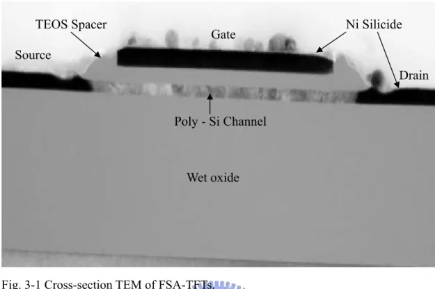
At first, the cross-section TEM of FSA-TFTs (un-doped gate RTA 550°C 30-sec) is shown in Fig.3-1. Thicknesses of channel film, TEOS oxide and gate are shown in Fig.3-2. In this chapter, the electrical characteristics of control TFTs and FSA-TFTs (in-situ doped gate) with RTA 550°C 30-sec are compared at first in 3.1. Then the electrical characteristics of control TFTs and FSA-TFTs (un-doped gate) with RTA 550°C 30-sec are compared in 3.2. Device parameters including parasitic resistance (RP), threshold voltage (VTH), subthreshold swing (S.S.), field-effect mobility (µFE),
ON current (ION), OFF current (IOFF), and ON/OFF current ratio are all extracted. Next
step, we will explain the electrical characteristics of control TFTs and FSA-TFTs. We found that S/D fully salicidation resulted in the reduction of VTH、kink effect、
threshold voltage roll off、subthreshold swing roll off and Gate-Induced-Drain- Leakage (GIDL) enhancement current.
3.1 Basic electrical characteristics of FSA-TFTs (in-situ
doped gate)
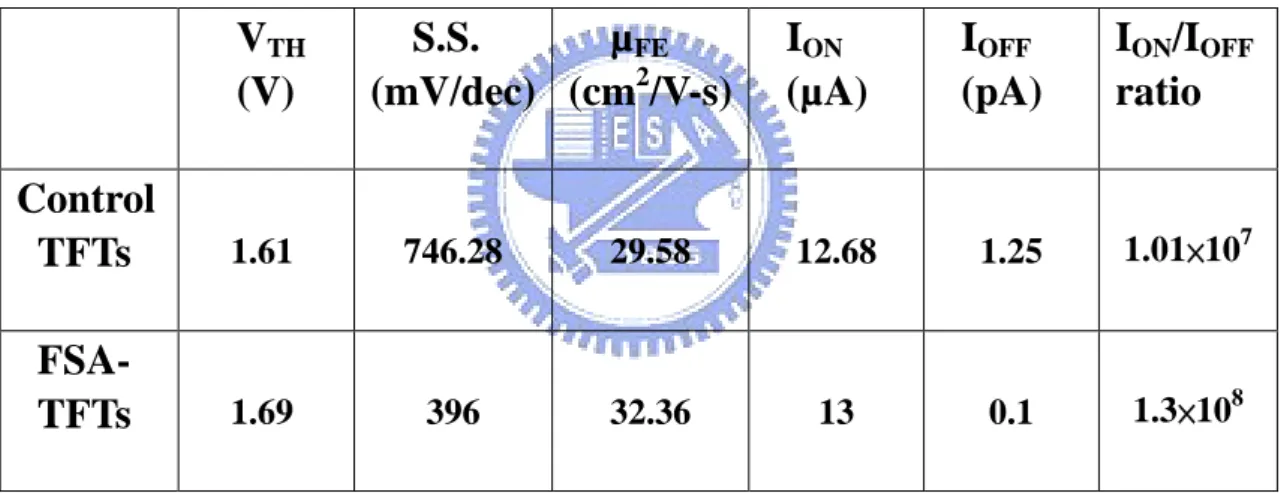
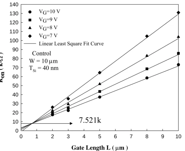
value of RP is 7.521 kΩ. Figure 3-4 shows the parasitic resistance (RP) of the
FSA-TFTs. The extracted value of RP is 0.7965 kΩ. Obviously, the RP of the
FSA-TFTs is significantly lower than that of the control TFTs.
Figure 3-5 exhibits ID-VG and field-effect mobility characteristics of control
TFTs with W/L=10 µm/10 µm and Tox=500 Å. The drain bias is 0.5 V and 5.0 V. The
ON current (ION) at VD=0.5 V and VG=15 V of control TFTs is 12.68 µA. The OFF
current (IOFF,the minimum value of drain current) of control TFTs is 1.25 pA. So, the
ON/OFF current ratio (ION/IOFF) is 1.01×10⁷. The maximum mobility of control TFTs
is 29.58 cm2/V-s.
Figure 3-6 exhibits ID-VG and field-effect mobility characteristics of the
FSA-TFTs with W/L=10 µm/10 µm and Tox=500 Å. The drain bias is 0.5 V and 5.0 V.
The ON current at VD=0.5 V and VG=15 V of FSA-TFTs is 14.44 µA. The OFF
current of FSA-TFTs is 0.1 pA. So, the ON/OFF current ratio is 1.444×10⁸. The maximum mobility of the FSA-TFTs is 33.96 cm2/V-s. Based on the above electrical results, significant improvements can be found for the FSA-TFTs. All devices’ parameters of the control TFTs and the FSA-TFTs are listed in the Table 3-1.
Figure 3-7 shows the comparison of ID-VG characteristics at VD=0.5 V between
control TFTs and FSA-TFTs with W/L=10 µm/10 µm. Figure 3-8 shows the comparison of mobility between control TFTs and FSA-TFTs with W/L =10 µm/10
µm. Fully Ni-salicidation remarkably improves the mobility of TFTs. From Table 3-1, FSA-TFTs give smaller threshold voltage, higher mobility, higher ON current and higher ON/OFF current ratio.
Figure 3-9 show ID-VD characteristics of control TFTs and FSA-TFTs with W/L
=10 µm/10 µm (VG-VTH=3.0 V, 4.0 V, 5.0 V, 6.0 V). The output current of FSA-TFTs
is obviously larger than that of control TFTs. The low parasitic resistance by fully Ni- salicidation greatly boosts the output current.
Figure 3-10 shows ID-VD output characteristics of control TFTs and FSA-TFTs
with W/L=10 µm/0.8 µm. The output characteristics exhibit in fact an anomalous current increase in the saturation region. The kink effect [31-32] is observed. The detailed explanation about the kink effect is shown in 3.3.2.
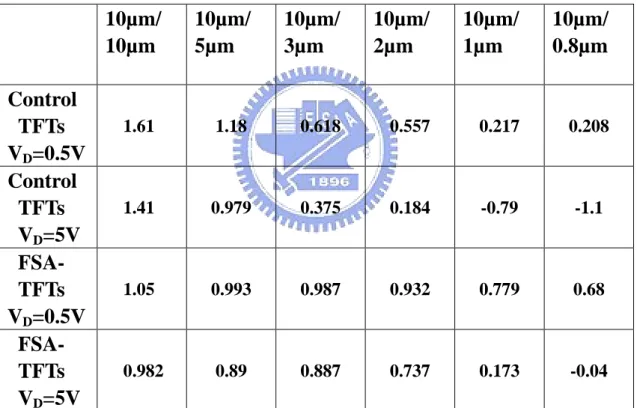
Figure 3-11 exhibits VTH roll off characteristics of control TFTs and FSA-TFTs.
All threshold voltages of control TFTs and FSA-TFTs are summarized in Table 3-2. The threshold voltage roll off from 10 µm to 0.8 µm of control TFTs at VD=0.5 V is
1.402 V. The threshold voltage roll off from 10 µm to 0.8 µm of FSA-TFTs at VD=0.5
V is 0.37 V. Obviously, threshold voltage roll off phenomenon of control TFTs is more severe than that of FSA-TFTs. Because the floating body effect of control TFTs is more severe than that of FSA-TFTs. So, VTH roll off phenomenon of control TFTs is
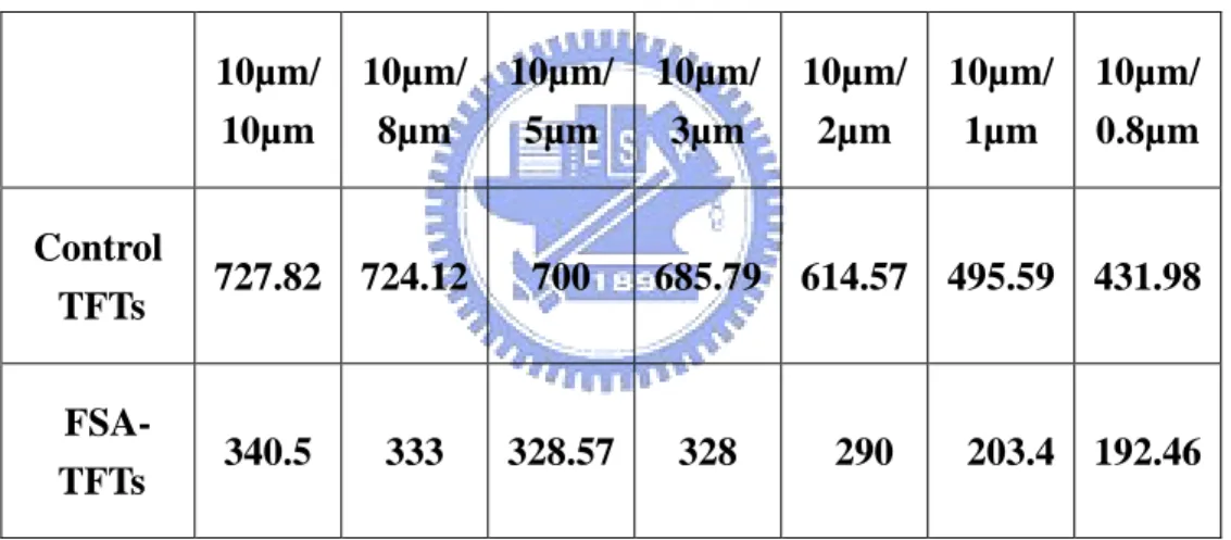
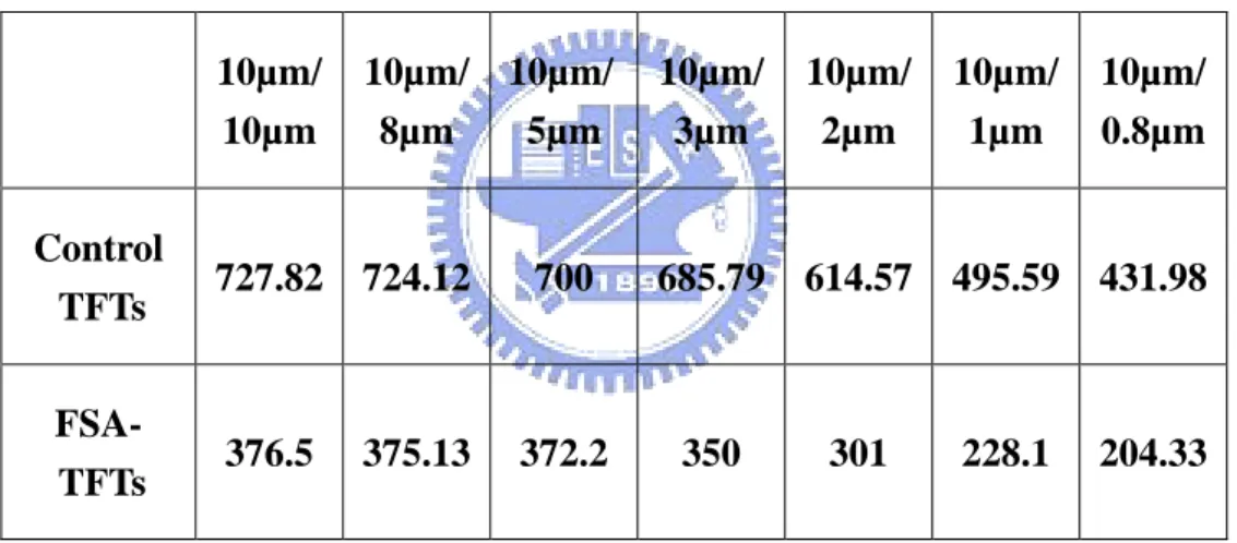
Figure 3-12 exhibits subthreshold swing (S.S.) roll off characteristics of control TFTs and FSA-TFTs. The drain bias is 5 V. The channel width is 10 µm. The S.S. roll off from 10 µm to 0.8 µm of control TFTs at VD=5 V is 295.84 mV/dec. The S.S. roll
off from 10 µm to 0.8 µm of FSA-TFTs at VD=5 V is 148.04 mV/dec. Table 3-3 shows
detailed data about subthreshold swing from 10 µm to 0.8 µm. Obviously, S.S. roll off phenomenon of control TFTs is more severe than that of FSA-TFTs.
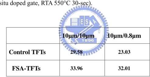
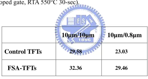
Figure 3-13 shows the mobility of control TFTs and FSA-TFTs when the channel length is 10 µm and 0.8 µm. The channel width is 10 µm. Table 3-4 shows detailed data about maximum mobility. The maximum mobility of FSA-TFTs are 33.96 cm2/ V-s and 32.01 cm2/V-s when the channel length is 10 µm and 0.8 µm. The degradation of mobility from 10 µm and 0.8 µm is 1.95 cm2/V-s. The maximum mobility of control TFTs is 29.58 cm2/V-s and 23.03 cm2/V-s when the channel length is 10 µm and 0.8 µm. The degradation of mobility from 10 µm and 0.8 µm is 6.55 cm2/V-s. Clearly, the mobility degradation of control TFTs is more severe than that of FSA- TFTs. This can be explained from Fig. 3-14. Where A is the channel length, B is the S/D regions. When channel length is decreased, the serious S/D resistance becomes prominent. This will result in the across voltage of the channel region becomes smaller. When the lateral electrical field becomes smaller, the mobility becomes smaller. But fully Ni-salicidation can result in the decrease of parasitic resistance. So,
the mobility roll off of FSA-TFTs from 10 µm to 0.8 µm is not severe.
The off-state leakage currents in n-type device are measured for channel length
of 10 µm and 0.8 µm at VG=-5 V as shown in Fig. 3-15. Obviously, the leakage
current of FSA-TFTs from 10 µm to 0.8 µm has little variation. However, the leakage current of control TFTs from 10 µm to 0.8 µm increases very quickly at VD=8 V. This
is because the fully Ni-salicidation can suppress parasitic BJT effect, the FSA-TFTs do not have severe GIDL enhancement current. About GIDL enhancement current is explained clearly in section 3.3.3.
3.2 Basic electrical characteristics of FSA-TFTs (un-doped
gate)
In this section, the electrical characteristics of control TFTs and FSA-TFTs (un-doped gate) with RTA 550°C 30-sec are compared.
The parasitic resistance (RP) of the control TFTs is 7.521 kΩ. Figure 3-16 shows
the parasitic resistance (RP) of the FSA-TFTs. The value of RP is 0.7224 kΩ.
Obviously, the RP of the FSA-TFTs with un-doped gate is much lower than that of the
control TFTs.
Figure 3-17 exhibits ID-VG and field-effect mobility characteristics of the
The ON current at VD=0.5 V and VG=15 V of FSA-TFTs is 13 µA. The OFF current
of FSA-TFTs is 0.1 pA. So, the ON/OFF current ratio is 1.3×10⁸. The maximum mobility of the FSA-TFTs is 32.36 cm2/V-s. All devices’ parameters of the control TFTs and the FSA-TFTs are listed in the Table 3-5. Similar to the results of device with doped gate, ON current, ON/OFF current ratio, the maximum mobility of FSA-TFTs with un-doped gate is higher than those of control TFTs.
Figure 3-18 shows the comparison of ID-VG characteristics at VD=0.5 V between
control TFTs and FSA-TFTs with W/L=10 µm/10 µm. Figure 3-19 shows the comparison of mobility between control TFTs and FSA-TFTs with W/L =10 µm/10 µm. The fully Ni-salicidation remarkably improves the mobility of TFTs.
Figure 3-20 show ID-VD characteristics of control TFTs and FSA-TFTs with
W/L= 10 µm/10 µm (VG-VTH=3.0 V, 4.0 V, 5.0 V, 6.0 V). The output current of FSA-
TFTs is obviously larger than that of control TFTs.
Figure 3-21 shows ID-VD output characteristics of control TFTs and FSA-TFTs
with W/L=10 µm/0.8 µm. The kink effect is observed.
Figure 3-22 exhibits VTH roll off characteristics of control TFTs and FSA-TFTs.
All threshold voltages of control TFTs and FSA-TFTs are summarized in Table 3-6. The threshold voltage roll off from 10 µm to 0.8 µm of control TFTs at VD=0.5 V is
V is 0.48 V. Obviously, threshold voltage roll off phenomenon of control TFTs is more severe than that of FSA-TFTs.
Figure 3-23 shows subthreshold swing (S.S.) roll off characteristics of control TFTs and FSA-TFTs. The drain bias is 5 V. The channel width is 10 µm. Table 3-7 shows detailed data about subthreshold swing from 10 µm to 0.8 µm. The S.S. roll off from 10 µm to 0.8 µm of control TFTs at VD=5 V is 295.84 mV/dec. The S.S. roll off
from 10 µm to 0.8 µm of FSA-TFTs at VD=5 V is 172.17 mV/dec. Obviously, S.S. roll
off phenomenon of control TFTs is more severe than that of FSA-TFTs.
Figure 3-24 shows the mobility of control TFTs and FSA-TFTs when the channel length is 10 µm and 0.8 µm. The channel width is 10 µm. Table 3-8 shows detailed data about maximum mobility. The maximum mobility of FSA-TFTs is 32.36 cm2/V-s and 29.46 cm2/V-s in the channel length of 10 µm and 0.8 µm. The degradation of mobility from 10 µm and 0.8 µm is 2.9 cm2/V-s. The degradation of mobility from 10 µm and 0.8 µm is 6.55 cm2/V-s in the control TFTs. Clearly, the mobility degradation of control TFTs is more severe than that of FSA-TFTs.
The off-state leakage currents in n-type device are measured for channel length
of 10 µm and 0.8 µm at VG=-5 V as shown in Fig. 3-25. Obviously, the leakage
current of FSA-TFTs from 10 µm to 0.8 µm has much less variation. However, the leakage current of control TFTs from 10 µm to 0.8 µm increases significantly at VD=8
V. So, the FSA-TFTs does not have severe GIDL enhancement current.
Figure 3-26 shows the GIDL enhancement current for in-situ doped gate and un-doped gate FSA-TFTs with W/L=10 µm/10 µm. The gate voltage is -5 V. The GIDL enhancement current of FSA-TFTs (un-doped gate) is higher than that of FSA -TFTs (in-situ doped gate). The doping of the poly-Si gate prior to complete gate silicidation affects the NiSi workfunction. The different dopant’s amount can tune the work function of NiSi [29]. Different work function of NiSi results in the larger leakage for FSA-TFTs with un-doped gate.
3.3 Analysis of the poly-Si TFT’s electrical characteristics
In this section, some electrical characteristics of devices will be discussed,
including the reduction of VTH using the S/D fully salicidation processes, kink effect,
Gate-Induced-Drain-Leakage (GIDL) enhancement current.
3.3.1 The reduction of V
THusing the S/D fully salicidation processes
Fully Ni-salicidation in the S/D region can result in the reduction of the threshold voltage. In the following, a equivalent circuit model is used to explain this phenomenon in Fig.3-27 [33]. A source resistance RS and a drain resistance RD are
assumed to connect an intrinsic TFT to the external terminals where VDS and VG are
relations are :
V’DS=VDS-(RS+RD)IDS--- (Eq. 3.1)
V’G=VG-RS×IDS--- (Eq. 3.2)
As shown in Fig. 3-27, an actual device with parasitic resistance is equivalent to an intrinsic TFT with a grounded source, with V’G and V’DS at the gate and the drain
terminals, and with a negative bias –RSIDS on the substrate. A negative bias on the
substrate leads to the body effect. This phenomenon results in the higher threshold voltage.
Fully Ni-salicide in the S/D region can result in the drastic decrease of the series resistance RS and RD. Therefore, the negative bias on the substrate is decreased and
the body effect is alleviated. So, the threshold voltage of TFTs could be reduced by the Ni-salicidation process.
3.3.2 Kink effect
The output characteristics exhibit an anomalous current increase in the saturation region. The kink effect is observed. The kink effect in TFTs is showed in Fig. 3-28. The short gate length and high drain bias result in the lateral electric field becomes stronger. The stronger lateral electric field causes impact ionization near the drain, generating more electron-hole pairs. Due to impact ionization occurring at the drain end of the channel, holes are injected into the floating body. The presence of these holes raises the body potential, which may become large enough to forward bias the
body-source. The hole current flowing into the source forces the electron injection from the source into the body. These electrons flow along the electric field into the drain region. This added drain current augments impact ionization which forward biases the floating body harder. The entire process is like a positive feedback to make the problem serious.
Because FSA-TFT’s source region can be used as a sink for holes [30], holes in
the floating body do not accumulate. So, FSA-TFT’s kink effect is not more severe than that of control TFTs.
3.3.3 Gate-Induced-Drain-Leakage (GIDL) enhancement current
GIDL is the off-state leakage current, which occurs when the gate potential is very low or negative and a high drain potential is applied [34]. The leakage current is the tunneling current in the deep depletion region due to the high vertical electric field. Fig. 3-29 shows the energy band diagram about the tunneling current. The tunneling theory predicts that
ID=AESexp(-B/ES) --- (Eq. 3.3)
Where A is a pre-exponential constant and B has a theoretical value of 21.3MV/cm. ES is the surface electric field.
In the n-type TFTs, holes generated on the surface of drain by band-to-band tunneling mechanism are swept into the floating body. The floating body potential
rises and becomes forward biased with respect to source (i.e. as emitter). The parasitic npn bipolar therefore enters into forward active mode. The GIDL current, thus, serves as the base current for the lateral bipolar transistor as shown in Fig. 3-30. The resultant current near the drain junction is thus given by
ID=βIGIDL+IGIDL=(β+1)IGIDL--- (Eq. 3.4)
Where β is the gain of the lateral BJT.
The current gain of the lateral BJT increases as the base width decreases. Therefore, for short channel devices, β is significant, which is not the case with long channel devices. In our above result, we have shown that control TFT’s GIDL current from 10 µm to 0.8 µm is more severe than that of FSA-TFTs. Hence, Ni-salicidation has demonstrated as a very promising technology to eliminate this lateral bipolar transistor effect.
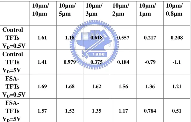
Table 3-1 Summary of parameters of control TFTs and FSA-TFTs (in-situ
doped gate, RTA 550°C 30-sec) with W/L=10 µm/10 µm and V
D=0.5 V.
V
TH(V)
S.S.
(mV/dec)
µ
FE(cm
2/V-s)
I
ON(µA)
I
OFF(pA)
I
ON/I
OFFratio
Control
TFTs
1.61 746.28 29.58 12.68 1.25 1.01×10⁷FSA-
TFTs
1.05 371.71 33.96 14.44 0.1 1.44×10⁸Table 3-2 V
TH(V) roll off of control TFTs and FSA-TFTs (in-situ doped
gate, RTA 550°C 30-sec).
10µm/
10µm
10µm/
5µm
10µm/
3µm
10µm/
2µm
10µm/
1µm
10µm/
0.8µm
Control
TFTs
V
D=0.5V
1.61 1.18 0.618 0.557 0.217 0.208Control
TFTs
V
D=5V
1.41 0.979 0.375 0.184 -0.79 -1.1FSA-
TFTs
V
D=0.5V
1.05 0.993 0.987 0.932 0.779 0.68FSA-
TFTs
V
D=5V
0.982 0.89 0.887 0.737 0.173 -0.04Table 3-3 Subthreshold swing (mV/dec) roll off of control TFTs and FSA
-TFTs (in-situ doped gate, RTA 550°C 30-sec) with V
D=5 V.
10µm/ 10µm 10µm/ 8µm 10µm/ 5µm 10µm/ 3µm 10µm/ 2µm 10µm/ 1µm 10µm/ 0.8µm Control TFTs 727.82 724.12 700 685.79 614.57 495.59 431.98 FSA- TFTs 340.5 333 328.57 328 290 203.4 192.46
Table 3-4 Maximum mobility (cm
2/V-s) of control TFTs and FSA-TFTs
(in-situ doped gate, RTA 550°C 30-sec).
10µm/10µm 10µm/0.8µm
Control TFTs
29.58 23.03Table 3-5 Summary of parameters of control TFTs and FSA-TFTs (un-
doped gate, RTA 550°C 30-sec) with W/L=10 µm/10 µm and V
D=0.5 V.
V
TH(V)
S.S.
(mV/dec)
µ
FE(cm
2/V-s)
I
ON(µA)
I
OFF(pA)
I
ON/I
OFFratio
Control
TFTs
1.61 746.28 29.58 12.68 1.25 1.01×10⁷FSA-
TFTs
1.69 396 32.36 13 0.1 1.3×10⁸Table 3-6 V
TH(V) roll off of control TFTs and FSA-TFTs (un-doped gate,
RTA 550°C 30-sec).
10µm/
10µm
10µm/
5µm
10µm/
3µm
10µm/
2µm
10µm/
1µm
10µm/
0.8µm
Control
TFTs
V
D=0.5V
1.61 1.18 0.618 0.557 0.217 0.208Control
TFTs
V
D=5V
1.41 0.979 0.375 0.184 -0.79 -1.1FSA-
TFTs
V
D=0.5V
1.69 1.68 1.62 1.56 1.36 1.21FSA-
TFTs
V
D=5V
1.57 1.52 1.35 1.17 0.784 0.51Table 3-7 Subthreshold swing (mV/dec) roll off of control TFTs and
FSA-TFTs (un-doped gate, RTA 550°C 30-sec) with V
D=5 V.
10µm/ 10µm 10µm/ 8µm 10µm/ 5µm 10µm/ 3µm 10µm/ 2µm 10µm/ 1µm 10µm/ 0.8µm Control TFTs 727.82 724.12 700 685.79 614.57 495.59 431.98 FSA- TFTs 376.5 375.13 372.2 350 301 228.1 204.33
Table 3-8 Maximum mobility (cm
2/V-s) of control TFTs and FSA-TFTs
(un-doped gate, RTA 550°C 30-sec).
10µm/10µm 10µm/0.8µm
Control TFTs
29.58 23.03Fig. 3-1 Cross-section TEM of FSA-TFTs.
Fig. 3-2 Thickness of Poly-Si channel film, Gate oxide and NiSi gate.
Ni Silicide TEOS Spacer Poly - Si Channel Wet oxide Gate Source Drain
Poly - Si Channel
Gate Oxide
NiSi Gate
Control
W = 10 µm
T
Si= 40 nm
Gate Length L (
µm )
0 1 2 3 4 5 6 7 8 9 10R
on
(
k-Ω
)
0 10 20 30 40 50 60 70 80 90 100 110 120 130 140 VG=10 V VG=9 V VG=8 V VG=7 VLinear Least Square Fit Curve
7.521k
FSA-TFTs
in-situ doped gate
W = 10 µm
T
Si= 40 nm
Gate Length L (
µm )
-1 0 1 2 3 4 5 6 7 8 9 10R
on
(
k-Ω
)
-10 0 10 20 30 40 50 60 70 80 90 100 VG=10 V VG=9 V VG=8 V VG=7 VLinear Least Squre Fit Curve
0.7965 k
Fig. 3-4 Parasitic resistance RP is extracted from the ID-VG of FSA-TFTs (in-situ
Control
VD=0.5 V,5.0 V
W/L=10 µm/10 µm
TSi = 40 nm
Gate Voltage VG ( V )
-5 0 5 10 15Drain Current I
D
( A )
10-13 10-12 10-11 10-10 10-9 10-8 10-7 10-6 10-5 10-4 10-3Field-Effect Mobility
µ
FE( cm
2/V-s )
0 10 20 30 40 50 ID-VG Field-Effect MobilityFig. 3-5 ID-VG and field-effect mobility characteristics of control TFTs with W/L=10
FSA-TFTs
In-situ doped gate
V
D=0.5 V,5.0 V
W/L=10 µm/10 µm
T
Si= 40 nm
Gate Voltage VG ( V )
-5 0 5 10 15Drain Current I
D
( A )
10-14 10-13 10-12 10-11 10-10 10-9 10-8 10-7 10-6 10-5 10-4 10-3Field-E
ffect Mobility
µ
FE( cm
2/V-s )
0 10 20 30 40 50 ID-VG Field-Effect MobilityFig. 3-6 ID-VG and field-effect mobility characteristics of FSA-TFTs (in-situ doped
VD=0.5 V
W/L=10 µm/10 µm
TSi = 40 nm
Gate Voltage VG ( V )
-5 0 5 10 15Drain Current I
D
( A )
10-14 10-13 10-12 10-11 10-10 10-9 10-8 10-7 10-6 10-5 10-4 ControlFSA-TFTs with in-situ doped gate
Fig. 3-7 Comparison of ID-VG characteristics between control TFTs and FSA-TFTs
VD=0.5 V
W/L=10 µm/10 µm
TSi = 40 nm
Gate Voltage VG ( V )
-5 0 5 10 15Field-E
ffect Mobility
µ
FE( cm
2/V-s )
0 10 20 30 40 ControlFSA -TFTs with in-situ doped gate
Fig.3-8 The mobility is plotted versus gate voltage at VD=0.5V for both control TFTs
and FSA-TFTs (in-situ doped gate) with W/L=10 µm/10 µm. The peak mobility is 29.58 cm2/V-s for control TFTs and 33.96 cm2/V-s for FSA-TFTs.
VG-VTH=3 V,4 V,5 V,6 V
W/L=10 µm/10 µm
TSi = 40 nm
Drain Voltage VD ( V )
0 2 4 6 8Drain Current I
D
(
µA )
0 5 10 15 20 25 30 35FSA-TFTs with in-situ doped gate Control
Fig. 3-9 ID-VD characteristics of control TFTs and FSA-TFTs (in-situ doped gate) with
VG-VTH=0.5 V,1.0 V,1.5 V,2.0 V
W/L=10 µm/0.8 µm
TSi = 40 nm
Drain Voltage VD ( V )
0 1 2 3 4 5Drain Current I
D
( µ
A )
0 10 20 30 40 50 60 70FSA-TFTs with in-situ doped gate Control
Fig. 3-10 ID-VD output characteristics of control TFTs and FSA-TFTs (in-situ doped
gate) with W/L=10 µm/10 µm. VG-VTH=0.5 V, 1.0 V, 1.5 V, 2.0 V. Note that kink
V
THroll off
Comparsion
T
Si= 40 nm
Gate Length L (
µm )
0 2 4 6 8 10Threshold Voltage V
TH
( V )
-1.5 -1.0 -0.5 0.0 0.5 1.0 1.5 2.0FSA-TFTs with in-situ doped gate VD=0.5 V FSA-TFTs with in-situ doped gate VD=5 V Control VD= 0.5 V
Control VD= 5 V
Fig. 3-11 Threshold voltage roll off vs. channel length. The channel width is 10 µm. The drain voltage is 0.5 V and 5 V.
S.S. roll off
V
D=5 V
T
Si= 40 nm
Gate Length L (
µm )
0 2 4 6 8 10Subthreshold Sw
ing S.S. ( mV/dec )
0 100 200 300 400 500 600 700 800FSA-TFTs with in-situ doped gate Control
Fig. 3-12 Subthreshold Swing roll off vs. channel length. The channel width is 10 µm. The drain voltage is 5 V.
Gate Voltage VG ( V )
-5 0 5 10 15Field-E
ffect Mobility
µ
FE( cm
2/V-s )
0 10 20 30 40FSA-TFTs with in-situ doped gate 10/10
FSA-TFTs with in-situ doped gate 10/0.8
Control 10/10 Control 10/0.8
Mobility
T
Si= 40 nm
Fig.3-13 The mobility is plotted versus gate voltage for both control TFTs and FSA -TFTs (in-situ doped gate) with W/L=10 µm/10 µm and W/L=10 µm/0.8 µm.
Fig.3-14 Schematic structure of device layout
G
D
S
A BFig.3-15 The GIDL enhancement current for both control TFTs and FSA-TFTs (in- situ doped gate) with W/L=10 µm/10 µm and W/L=10 µm/0.8 µm.
GIDL Enhancement Current
VG= -5 V
TSi = 40 nm
Drain Voltage VD ( V )
0 2 4 6 8Drain Current I
D
( A )
10-14 10-13 10-12 10-11 10-10 10-9 10-8 10-7 10-6FSA-TFTs with in-situ doped gate 10/10 FSA-TFTs with in-situ doped gate 10/0.8 Control 10/10
Fig. 3-16 Parasitic resistance Rp is extracted from the ID-VG of FSA-TFTs (un-doped gate).
FSA-TFTs
un-doped gate
W = 10 µm
T
Si= 40 nm
Gate Length L (
µm )
-1 0 1 2 3 4 5 6 7 8 9 10 11 12R
on(
k-Ω
)
0 10 20 30 40 50 60 70 80 90 100 110 120 130 140 VG=10 V VG=9 V VG=8 V VG=7 VLinear Least Square Fit Curve
FSA-TFTs
un-doped gate
VD=0.5 V,5.0 V
W/L=10 µm/10 µm
TSi = 40 nm
Gate Voltage VG ( V )
-5 0 5 10 15Drain Current I
D
( A )
10-14 10-13 10-12 10-11 10-10 10-9 10-8 10-7 10-6 10-5 10-4 10-3Field-Effect Mobility
µ
FE( cm
2/V-s )
0 10 20 30 40 50 ID-VG Field-Effect MobilityFig. 3-17 ID-VG and field-effect mobility characteristics of FSA-TFTs (un-doped gate)
VD=0.5 V
W/L=10 µm/10 µm
TSi = 40 nm
Gate Voltage VG ( V )
-5 0 5 10 15Drain Current I
D
( A )
10-14 10-13 10-12 10-11 10-10 10-9 10-8 10-7 10-6 10-5 10-4 ControlFSA-TFTs with un-doped gate
Fig. 3-18 Comparison of ID-VG characteristics between control TFTs and FSA-TFTs
Gate Voltage VG ( V )
-5 0 5 10 15Field-Effect Mobility
µ
FE( cm
2/V-s )
0 10 20 30 40FSA-TFTs with un-doped gate Control
VD=0.5 V
W/L=10 µm/10 µm
TSi = 40 nm
Fig.3-19 The mobility is plotted versus gate voltage at VD=0.5 V for both control
TFTs and FSA-TFTs (un-doped gate) with W/L=10 µm/10 µm. The peak mobility is 29.58 cm2/V-s for control TFTs and 32.36 cm2/V-s for FSA-TFTs.
VG-VTH=3 V,4 V,5 V,6 V
W/L=10 µm/10 µm
TSi = 40 nm
Drain Voltage VD ( V )
0 2 4 6 8Drain Current I
D
(
µA )
0 5 10 15 20 25 30 35FSA-TFTs with un-doped gate Control
Fig. 3-20 ID-VD characteristics of control TFTs and FSA-TFTs (un-doped gate) with
VG-VTH=0.5 V,1.0 V,1.5 V, 2.0 V
W/L=10 µm/0.8 µm
TSi = 40 nm
Drain Voltage VD ( V )
0 1 2 3 4 5Drain Current I
D
(
µA )
0 10 20 30 40 50 60 70FSA-TFTs with un-doped gate Control
Fig. 3-21 ID-VD output characteristics of control TFTs and FSA-TFTs (un-doped gate)
with W/L=10 µm/10 µm. VG-VTH=0.5 V, 1.0 V, 1.5 V, 2.0 V. Note that kink effect is
VTH roll off
Comparsion
TSi = 40 nm
Gate Length L (
µm )
0 2 4 6 8 10Threshold Voltage V
TH
( V )
-1 0 1 2FSA-TFTs with un-doped gate VD=0.5 V FSA-TFTs with un-doped gate VD=5 V Control VD= 0.5 V
Control VD=5 V
Fig. 3-22 Threshold voltage roll off vs. channel length. The channel width is 10 µm. The drain voltage is 0.5 V and 5 V.
S.S. roll off
VD = 5 V
TSi = 40 nm
Gate Length L (
µm )
0 2 4 6 8 10Subthreshold Sw
ing S.S. ( mV/dec )
0 100 200 300 400 500 600 700 800FSA-TFTs with un-doped gate Control
Fig. 3-23 Subthreshold swing roll off vs. channel length. The channel width is 10 µm. The drain voltage is 5 V.
Gate Voltage VG ( V )
-5 0 5 10 15Field-E
ffect Mobility
µ
FE( cm
2/V-s )
0 10 20 30 40FSA-TFTs with un-doped gate 10/10 FSA-TFTs with un-doped gate 10/0.8 Control 10/10
Control 10/0.8
Mobility
TSi = 40 nm
Fig.3-24 The mobility is plotted versus gate voltage for both control TFTs and FSA- TFTs (un-doped gate) with W/L=10 µm/10 µm and W/L=10 µm/0.8 µm.
Fig.3-25 The GIDL enhancement current for both control TFTs and FSA-TFTs (un-doped gate) with W/L=10 µm/10 µm and W/L=10 µm/0.8 µm.
GIDL Enhancement Current
VG= -5 V
TSi = 40 nm
Drain Voltage VD ( V )
0 2 4 6 8Drain Current I
D
( A )
10-14 10-13 10-12 10-11 10-10 10-9 10-8 10-7 10-6FSA-TFTs with un-doped gate 10/10 FSA-TFTs with un-doped gate 10/0.8 Control 10/10
GIDL Enhancement Current
VG= -5 V
TSi = 40 nm
Drain Voltage VD ( V )
0 2 4 6 8Drain Current I
D
( A )
10-14 10-13 10-12 10-11 10-10 10-9 10-8 10-7FSA-TFTs with in-situ doped gate 10/10 FSA-TFTs with un-doped gate 10/10
Fig. 3-26 The GIDL enhancement current for in-situ doped gate and un-doped gate FSA-TFTs with W/L=10 µm/10 µm.
Fig.3-27 Equivalent circuit model with S/D series resistance is shown. The intrinsic part of the top circuit is equivalent to the bottom circuit with redefined terminal voltages [33].
V’
GR
SR
DV
DSI
DSV’
DSV’
G=V
G-R
S*I
DSI
DS-R
S*I
DSV’
DS=V
DS-(R
S+R
D)I
DSFig. 3-28 The kink effect in Poly-Si TFTs.
V
SV
GBuried Oxide
n+ n+
V
D
Fig. 3-29 Energy band diagram between gate and drain terminals.
Tunneling
Electron
Fig. 3-30 Schematic of n-type poly-Si TFTs current flow in GIDL mode when the channel is turned off.
Buried Oxide
βI
GIDLV
Dn+ n+
V
SI
GIDLV
GChapter 4
Conclusions and Future works
4.1 Conclusions
In this thesis, we have investigated, for the first time, the fully Ni-salicided S/D and Gate in poly-Si TFTs. For fully Ni-salicidation technique, the parasitic resistance is drastically decreased. Besides its low resistivity, NiSi also possesses some inherent properties: (1)NiSi does not have narrow line effect. (2)Nickel is not reacted with oxide. (3)NiSi has the less silicon consumption compared with TiSi2 and CoSi2.
(4)Silicidation can be formed at low temperature (400~600°C) without agglomeration. In this thesis, fully Ni-salicided S/D and Gate can be achieved by one step RTA 550°C for 30-sec. The FSA-TFTs have excellent performance. Take in-situ doped gate for example, the ON current of FSA-TFTs is 14.44 µA. The OFF current of FSA-TFTs is 0.1 pA. So, the ON/OFF current ratio can be reached as high as 1.444×10⁸ which is one order of magnitude higher than control ones. The maximum mobility of the FSA-TFTs can also be achieved as high as 33.96 cm2/V-s.
It is demonstrated that fully Ni-salicidation is a technology to solve some problems in this thesis. FSA-TFTs can effectively suppress the floating-body effect and parasitic bipolar junction transistor action, compared to control TFTs.
Experimental results show that the FSA-TFTs give lower off-state leakage, improved subthreshold characteristics, less threshold voltage variation, and larger field-effect mobility compared with control TFTs. The characteristics of the FSA-TFTs are suitable for high performance driving TFTs with a stable threshold voltage and large breakdown voltage.
4.2 Future works
There are some interesting and important topics that are valuable for the future
works. First of all, SPC process is used to crystallize a-Si layer in this thesis. Low mobility and high trap state density are the two major disadvantages. With excimer laser crystallization (ELC), better device performance can be expected. Besides active layer crystallization, there are many different process conditions which are our future works.
Different S/D implant dosage is an interesting topic. In this thesis, the S/D implant dosage is 5×1015 cm-2. Different S/D implant dosage include 1×1015cm-2, 5× 1014 cm-2, 1×1014 cm-2 can be executed. We expect that fewer S/D implant dosages will not have severe kink effect, compared to control TFTs.
In-situ doped gate and un-doped gate FSA-TFTs have been successfully fabricated. Different gate implant dosage is also an interesting topic that we want to accomplish.
We hope that the different threshold voltage in the different gate implant dosage can be observed. Different RTA temperature, different RTA time, different TEOS oxide spacer thickness and 300 Å of channel film thickness are also our future research topics.
References :
[1] Z. Shengdong, Z. Chunxiang, J. K. O. Sin, J. N. Li, and P. K. T. Mok, ”Ultra-thin elevated channel poly-Si TFT technology for fully-integrated AMLCD system on glass” IEEE Trans. Electron Devices, vol. 47, no. 3, pp.569-575, 2000.
[2] I. W. Wu, ”Low temperature poly-Si TFT technology for AMLCD’s” Proc. 1995 Int. Workshop on Active-Matrix Liquid-Crystal Displays, Osaka, Japan, 1995.
[3] I. W. Wu, A. G. Lewis, T. Y. Huang, and A. Chiang, ”Effects of trap-state density reduction by plasma hydrogenation in low-temperature polysilicon TFT” IEEE Electron Device Lett., vol. 10, no. 3, pp123-125, 1989.
[4] F. S. Wang, M. J. Tsai, and H. C. Cheng, ”The effects of NH3 plasma passivation
on polysilicon thin-film transistors” IEEE Electron Device Lett., vol. 16, no. 11, pp503-505, 1995.
[5] C. F. Yeh, D. C. Chen, C. Y. Lu, C. Liu, S. T. Lee, C. H. Liu, and T. J. Chen,”Highly reliable liquid-phase deposited SiO2 with nitrous oxide plasma
post-treatment for low temperature processed poly-Si TFTs” IEDM Tech. Dig., pp.269-272, 1998.
[6] S. Ikeda, S. Hashiba, I. Kuramoto, H. Katoh, S. Ariga, T. Yamanaka, T. Hashimoto, N. Hashimoto, and S. Meguro, ”A polysilicon transistor technology for large capacity

![TraditionalMLCalgorithmsmainlytacklethebatchMLCproblem,wheretheinputdataarepresentedinabatch[24,28].Nevertheless,inmanyMLCapplicationssuchase-mailcategorization[22],multi-labelexamplesarriveasastream.Onlineanalysisistherefore dimensionreducermotivatedbyma](data:image/gif;base64,R0lGODlhAQABAIAAAP///wAAACH5BAEAAAAALAAAAAABAAEAAAICRAEAOw==)