國
立
交
通
大
學
電子工程學系 電子研究所
碩
士
論
文
超低動態電壓基於頻率比之製程、電壓、溫度感測器
與其應用
Ultra-low Dynamic Voltage Scaling
Fequency-Ratio-Based PVT Sensor Design and
Applications
研 究 生:林上圓
指導教授:黃 威 教授
超低動態電壓基於頻率比之製程、電壓、溫度感測器
與其應用
Ultra-low Dynamic Voltage Scaling Frequency-Ratio-Based
PVT Sensor Design and Applications
研 究 生:林上圓 Student:Shang-Yaun Lin
指導教授:黃 威 教授 Advisor:Prof. Wei Hwang
國 立 交 通 大 學
電 子 工 程 學 系 電 子 研 究 所
碩 士 論 文
A Thesis
Submitted to Department of Electronics Engineering & Institute of Electronics College of Electrical Engineering and Computer Engineering
National Chiao Tung University in partial Fulfillment of the Requirements
for the Degree of Master
in
Electronics Engineering September 2011
Hsinchu, Taiwan, Republic of China
I
超低動態電壓基於頻率比之製程、電壓、溫度感測器
與其應用
學生:林上圓
指導教授:黃 威 教授
國立交通大學電子工程學系電子研究所
摘 要
隨著製程不斷微縮,高密度的積體電路造成自我加熱的問題。為了有效進行 溫度管理,本論文提出了一種適應性電壓選擇的製程電壓溫度變異感測器,其操 作的電壓範圍從 0.25 V〜0.5V,具備了 2.3μW 功耗和 50K 採樣 /秒的轉換率。 接著,0.4V 的完全晶上抗製程變異溫度感測器被提出,製程變異造成的影響顯 著降低。該電路經過實現且運作在 0.4V 電源電壓下,運行的溫度範圍為 0˚C 至 100˚C。此溫度感測器核心面積(不包括 輸入/輸出阜)只有 990μm2 。電力消耗 量的轉換率是 11.6μJ/採樣。所有這些特點使溫度感測器適用於能源有限與能源 收穫微型便攜式平台。最後,三維集成電路(3D- IC)架構被提出。為了防止內 部各層的熱點效應與減少動態隨機存取記憶體刷新功率,我們運用抗製程變異溫 度感測器,提出了一個動態隨機存取記憶體刷新控制器。由於溫度感測器功耗很 小,刷新控制器之額外功率不大,且有效減少 67.67%之待機功耗。II
Ultra-low Dynamic Voltage Scaling
Frequency-Ratio-Based PVT Sensor Design and
Applications
Student: Shang-Yaun Lin
Advisor: Prof. Wei Hwang
Department of Electronics Engineering & Institute of Electronics
National Chiao-Tung University
ABSTRACT
With process scaling down continuously, high level of integration introduces the problem of self-heating. To perform thermal management, this thesis proposes 0.5V~0.25V process voltage and temperature (PVT) sensors with adaptive voltage selection operating over an ultra-low supply voltage range from 0.25V~0.5V with 2.3μW power consumption and 50k samples/sec conversion rate. Next, the 0.4V fully integrated process invariant temperature sensor is proposed. The effect of process variation is significantly reduced. The realization meets the target to be capable of 0.4V supply voltage operation over the temperature range of 0˚C to 100˚C. The area of the sensor core (without I/O pads) is only 990μm2. The power consumption per conversion rate is 11.6pJ/sample. The high area/energy efficiency characteristics make the proposed sensor applicable for energy-limited miniature portable platforms. Finally, the heterogeneous three dimension integrated circuit (3D-IC) architecture is presented. To prevent hot spot on the intra layer and reduce refresh power on DRAM layer, we proposed a DRAM refresh controller utilizing the process invariant temperature sensor. Thanks for tiny power consumption of temperature sensors, the refresh controller reduces standby power significantly, 67.67% without much power overhead.
III
Acknowledgements
感謝許多人的幫助,讓我完成了這一篇論文。 首先我要感謝我的指導教授黃威老師在這兩年來的指導和鼓勵,在研究過程 中提供了許多方向和建議,在老師指導下讓我對研究有更深入的了解,也建立了 研究的興趣。此外老師提供的研究資源與自由的研究環境,讓我能夠充分發揮自 己的能力完成論文。 感謝實驗室的學長與同學們,這兩年來的幫忙。感謝張銘宏、黃柏蒼、楊皓 義三位學長在我的研究上的協助,特別是張銘宏學長在論文和研究上的鼎力相 助。此外也感謝其他實驗室夥伴們平時的互相 Cover,讓我在眾多科目夾擊之下 可以全身而退。 最後要感謝一直支持我的家人和朋友們,讓我可以克服論文壓力,順利完成 碩士的論文研究。IV
Content
Chapter 1 Introduction ... 1
1.1 Motivation ... 1
1.2 Research Goal and Major Contributions... 3
1.3 Thesis Organization ... 4
Chapter 2 Previous Works of Temperature Sensors ... 6
2.1 Introduction ... 6
2.2 BJT Based Temperature Sensor ... 7
2.3 Analog CMOS Based Temperature Sensor ... 14
2.4 Delay Based Temperature Sensors ... 18
2.4.1 Time-to-Digital Converter Based Temperature Sensors ... 18
2.4.2 Dual-DLL-Based All-Digital Temperature Sensor ... 26
2.4.3 Sub-μW Embedded CMOS Temperature Sensor ... 28
2.5 Leakage Based Temperature Sensor ... 32
2.6 Frequency-to-Digital Converter Based Temperature Sensor ... 35
2.7 Summary ... 38
Chapter 3 0.5V~0.25V Process, Voltage and Temperature Sensors with Adaptive Voltage Selection ... 41
3.1 Introduction ... 41
3.2 Design Principles in Ultra-Low Voltage ... 43
3.2.1 Challenges of Temperature Sensor in Ultra-Low Voltage ... 43
3.2.2 Ultra-Low Voltage Frequency-Based Temperature Sensor ... 48
3.3 PVT Sensors with Adaptive Voltage Selection ... 51
3.3.1 Finite State Machine ... 52
3.3.2 Process and Voltage Sensor ... 54
3.3.3 Temperature Sensor ... 57
3.3.4 PV-Compensation ... 59
3.4 Simulation Results ... 61
3.5 Summary ... 63
Chapter 4 0.4V Fully Integrated Process Invariant Temperature Sensor ... 64
4.1 Introduction ... 64
4.2 Design Concepts of Process Invariant Temperature Sensor ... 65
4.3 Specific Architecture of Process Invariant Temperature Sensor ... 68
4.4 Simulation and Experimental Results ... 70
4.5 Summary ... 78
Chapter 5 Temperature-Aware DRAM Refresh Controller in TSV 3D-IC ... 79
V
5.2 Thermal Issues and Solutions in 3D-IC and DRAM Refresh ... 81
5.2.1 Thermal Issues in 3D-IC ... 81
5.2.2 The 3D-IC with Interlayer Cooling ... 83
5.2.3 Previous Works of DRAM Refresh Control ... 89
5.3 Heterogeneous 3D Integration ... 94
5.4 Temperature-Aware Refresh Controller of DRAM Layer ... 98
5.4.1 Data Retention Time Analysis ... 98
5.4.2 Proposed Refresh Control Scheme ... 101
5.4.3 Simulation Results ... 105
5.5 Summary ... 107
Chapter 6 Conclusions and Future Work ... 108
6.1 Conclusions ... 108
6.2 Future Work ... 109
VI
List of Tables
Table 2.1 Comparison of each type temperature sensors. ... 40
Table 3.1 Temperature sensor comparisons ... 62
Table 4.1 Performance Comparison of Recent Temperature Sensors. ... 77
VII
List of Figures
Figure 1.1 Sensor network of WBAN [1.10]. ... 2
Figure 2.1 Schematic of BJT based temperature sensor [2.13]. ... 8
Figure 2.2 Dual-slope integrating ADC for (a) genetic design, (b) timing diagram [2.13]. ... 9
Figure 2.3 Schematic of the thermal sensing system [2.13]. ... 11
Figure 2.4 Schematic of the front end sense stage with active cascode impedance enhancement, DEM and chopped currents in BJT pairs. Output VBE1 and VBE2 are routed to the input ADC input MUX [2.13]. ... 13
Figure 2.5 Illustration of the current chopping to up-convert the temperature signal to fchop [2.13]. ... 13
Figure 2.6 Conventional three-transistor temperature sensor [2.17]. ... 14
Figure 2.7 Conventional three-transistor temperature sensor [2.17]. ... 16
Figure 2.8 Four-transistor, voltage output, temperature sensor [2.18]. ... 17
Figure 2.9 Operating points of four-transistor temperature sensor [2.18]. ... 18
Figure 2.10 Block diagram of the time-to-digital temperature sensor [2.19]. ... 19
Figure 2.11 Temperature-to-pulse generator [2.19]. ... 19
Figure 2.12 Width offset reduction accomplished by delay line 2 [2.19]. ... 21
Figure 2.13 Operating points of four-transistor temperature sensor [2.19]. ... 21
Figure 2.14 Implemented architecture of the proposed smart temperature sensor [2.21]. ... 23
Figure 2. 15 Sensor output linearity for (a) temperature-insensitive and (b) curvature -compensating ARDL cell delay [2.21]. ... 24
Figure 2.16 Modified temperature compensation circuit for the ARDL delay cell [2.21]. ... 25
Figure 2.17 Basic architecture of DLL-based CMOS digital temperature sensor [2.22]. ... 27
Figure 2.18 Calibration mode (top) and measurement mode (bottom) [2.22]. ... 28
Figure 2.19 Block diagram of the proposed temperature sensor with interfacing in the RFID tag system [2.23]. ... 30
Figure 2.20 Block diagram of the proposed temperature sensor with interfacing in the RFID tag system [2.23]. ... 31
Figure 2.21 Simulated temperature modulated pulse width from -10 ˚C to 30 ˚C [2.23]. ... 32
VIII
Figure 2.23 Leakage current mechanisms in the thermal sensor [2.24]. ... 34
Figure 2.24 Implementation of the sensor along with the logarithmic counter [2.24]. ... 35
Figure 2.25 Block diagram of the temperature sensor proposed [2.25]. ... 36
Figure 2.26 Enhanced performance of temperature measurement with the TIO [2.25]. ... 36
Figure 2.27 Ring type oscillator with current starved delay cells [2.25]. ... 37
Figure 2.28 (a) Block diagram of a FDC and (b) timing diagram of the control signal [2.25]. ... 38
Figure 2.29 The fishbone diagram of temperature sensors. ... 39
Figure 2.30 Comparison of temperature sensors. ... 40
Figure 3.1 The DVFS system of energy harvesting. ... 42
Figure 3.2(a) Temperature-to-delay-difference generator.(b) Temperature-to-frequency-difference generator. ... 45
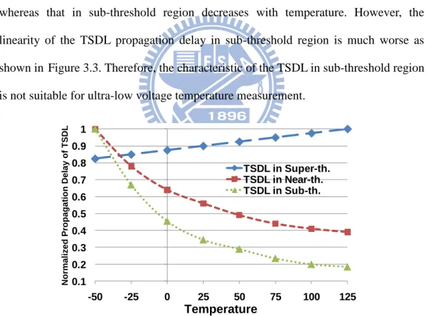
Figure 3.3 The linearity of temperature sensitive delay line (TSDL) in super-threshold, near-threshold and sub-threshold region. ... 46
Figure 3.4 (a) Ultra-low voltage frequency-based temperature sensor. (b) Inverter used in SB-TSRO. ... 48
Figure 3.5 (a) The relationship between temperature and threshold voltage. (b) The relationship of SB-TSRO output frequency versus temperature. ... 50
Figure 3.6 Architecture of proposed sensor. ... 52
Figure 3.7 State diagram of FSM. ... 53
Figure 3.8 Signal waveform diagram of FSM. ... 53
Figure 3.9 Implement circuit of FSM. ... 54
Figure 3.10 ZTC point simulation of NMOS and PMOS. ... 55
Figure 3.11 Implement circuit of PV sensor. ... 55
Figure 3.12 (a) The relationship between digital output and process variation.(b) The Monte Carlo simulation. ... 56
Figure 3.13 (a) Compensation circuits and mapping table of voltage sensor. (b) Voltage sensor digital output under variation. (c) Digital output after process compensation. ... 57
Figure 3.14 Implement circuit of temperature sensor. ... 58
Figure 3.15 Simulation results of temperature sensor. ... 59
Figure 3.16 PV-compensation circuits and compensation value tables. ... 60
Figure 3.17 Simulation results of compensated digital output. ... 61
IX
Figure 4.1 Block diagram of the proposed ultra-low voltage frequency-based
temperature sensor with process variation immunity enhancement. ... 65
Figure 4.2 The effect of process variation on the proposed process invariant temperature sensor. ... 68
Figure 4.3 The implementation of the proposed process invariant temperature sensor. ... 69
Figure 4.4 The timing diagram of the proposed process invariant temperature sensor. ... 70
Figure 4.5 (a) Digital output of sensor in post-layout simulation. (b) Simulated output error for 0˚C~100˚C. ... 71
Figure 4.6 Microphotograph of proposed process invariant temperature sensor .... 72
Figure 4.7 PCB board design. ... 73
Figure 4.8 Measurement environment for the test chips. ... 74
Figure 4.9 Bare die of the test chip on PCB board. ... 75
Figure 4.10 Measured error curves for 12 test chips. ... 76
Figure 4.11 Measured result curves for 12 test chips. ... 76
Figure 4.12 Measurement error curves for voltage variations. ... 77
Figure 5.1 3D circuit architecture connected to a conventional heat removal device [5.16]. ... 80
Figure 5.2 Temperature increase on the top die in a 3D chip-stack caused by a 100×100μm2 hot spot is approximately three times higher (red curve) than the temperature increase in a 2D SoC chip (blue curve) [5.10]. ... 82
Figure 5.3 Graphical interface of the thermal compact model for 3D stacked structures [5.10]. ... 83
Figure 5.4 Scheme of 3D-IC stack with microchannel [5.15]. ... 84
Figure 5.5 3D-IC with TSVs and inter-layer cooling channels that is enclosed in a sealed manifold [5.15]. ... 85
Figure 5.6 Two-layer 3D circuit layouts for evaluating the performance of micro -channel cooling. The areas occupied by memory and logic are the same and the logic dissipates 90% of the total power consumption [5.16]. ... 86
Figure 5.7 Comparison of junction temperatures in a two-layer stacked circuit for the cases of an integrated microchannel heat sink and a conventional heat sink. The total flow rate of the liquid water is 15 ml/min and the mass flux is 1.36 ×10⁻⁵ kg/s [5.16]. ... 89
Figure 5.8 Self-refresh and thermometer control scheme [5.17]. ... 90
Figure 5.9 Block diagram of a self-refresh scheme [5.17]. ... 92 Figure 5.10 Block diagram and timing diagram for the self-refresh period control
X
with temperature sensor [5.18]. ... 93
Figure 5.11 Heterogeneous integration of multi-core, SRAM, DRAM, front-end circuits stacking. ... 95
Figure 5.12 Detail floor planning of each layer. ... 96
Figure 5.13 Two steps of signal amplification. (a) Selected WL turning on and charge shared between Ccell and CBL. (b) Sense amplifier amplify small voltage swing of BL. ... 98
Figure 5.14 The data retention time of DRAM cell in different sensitivity of sense amplifier. ... 100
Figure 5.15 Monte-Carlo simulation of data retention time whenΔVBL =120mV. ... 101
Figure 5.16 (a) The DRAM layer in 3D-IC. (b) The refresh controller of DRAM sub-block. ... 103
Figure 5.17 (a) Refresh CLK generator. (b) The sense amplifier control circuit. . 104
Figure 5.18 The operation waveform of sub-block system. ... 105
Figure 5.19 Standby power analysis of 2Mb DRAM. ... 106
Figure 5.20 Standby power reduction of 2Mb DRAM. ... 107
Figure 6.1 Sub/near-threshold DVFS system. ... 110
1
Chapter 1
Introduction
1.1 Motivation
With the evolution of CMOS process technology, the number of transistors in a digital core doubles about every two years. The increases of transistor density and operating frequency have brought the effect of shorter battery life. For some applications such as wireless body area network (WBAN) sensors, the critical consideration is life time instead of operating speed. An important application of WBAN is the vital sensor network shown in Figure 1.1. Sensor nodes that measure biomedical signals such as electrocardiogram, blood pressure, and etc, are small pieces either attached on or implanted into a human body. They use a battery with as thin and light characteristics as possible. Most of them do not have the ability to last for a long time. Thus, how to perform a low-power design and meanwhile conform to the speed and reliability requirements is an important issue.
2
Figure 1.1 Sensor network of WBAN [1.10].
Ultralow-power dissipation can be achieved by operating digital circuits with scaled supply voltages, albeit with degradation in speed and increased susceptibility to parameter variations. The operating voltage is scaled down to sub-threshold or near-threshold regions depending on the power and speed requirements of circuit system. There are many researches about sub/near-threshold operation. [1.1] demonstrates optimizations of sub-threshold design in device, circuit as well as architecture perspectives, which are different from the conventional super-threshold design. [1.2] gives examples to show that designing flexibility into ultralow-power (ULP) systems across the architecture and circuit levels can meet both the ULP requirements and the performance demands. It also present a method that expands on ultra-dynamic voltage scaling (UDVS) to combine multiple supply voltages with component level power switches to provide more efficient operation at any energy-delay point and low overhead switching between points. The UDVS technique is described in [1.3], which presents voltage-scalable circuits such as logic cells, SRAMs, ADCs, and dc-dc converters. Using these circuits as building blocks, some applications have been highlighted.
3
Furthermore, dynamic voltage and frequency scaling (DVFS), achieves extremely efficient energy saving by adjusting system supply voltage and frequency depending on workload monitor [1.4]. Because of this reason, there are many previous researches about DVFS power management for digital systems such as RISC, DSP and Video Code. On the other hand, as we continue to reduce the voltage until the transistor get into the near/sub-threshold voltage, circuits will become more sensitive to Process, Voltage and Temperature (PVT) variations than super threshold. As a result, this thesis focuses on temperature sensor research which can operate at ultra-low dynamic voltage scaling (DVS).
On the other hand, a new class of package technologies, three-dimensional integrated circuit (3D-IC) [1.5], [1.6], for multi-function integration makes on-die hot spots even worse because of increasing power density and unbalanced thermal stresses distribution. Temperature variations over time induced by those stacking structures in 3D-IC require a fast and area-efficient temperature sensor to enable real-time multiple-location hot-spot detection. Also, in order to achieve small self-refresh current, the dynamic random access memory (DRAM) required on-chip thermometer with self-refresh scheme [1.7] - [1.9]. When a thermometer is implemented in a memory chip, many factors should be considered, including number, location, accuracy, area, and power consumption.
1.2 Research Goal and Major Contributions
The goal of this research is to design and implement ultra-low dynamic voltage scaling frequency-ratio-based PVT sensor for variation-aware DRAM refresh controller in 3D-IC. It includes 0.5V~0.25V PVT sensors with adaptive voltage
4
selection, 0.4V fully integrated process invariant temperature sensor and temperature-aware DRAM refresh controller in 3D-IC.
The major contributions of this thesis are list as follow:
1. The 0.5V~0.25V process, voltage and temperature sensors with adaptive voltage selection are proposed for temperature measurement in the energy harvesting DVFS systems. It composes of process, voltage and temperature sensors, providing process, voltage and temperature information. The process sensor and voltage (PV) sensor monitor the process variation and voltage variation continuously and give the variation information for temperature compensation.
2. A 0.4V fully integrated process invariant frequency-based temperature sensor is proposed. The effect of process variation is significantly reduced. Moreover, it consumes tiny power and occupies small area. Highly area and energy efficient is achieved.
3. The heterogeneous 3D-IC architecture is presented. To prevent hot spot on the intra layer and reduce DRAM refresh power, we proposed a refresh controller utilizing the process invariant temperature sensor. The controller reduces standby power significantly without much power overhead.
1.3 Thesis Organization
This thesis includes six chapters which focus on different temperature sensor design and its application such as: 3D-IC and DRAM refresh. The following briefly introduces the content of each chapter.
5
Chapter 2 gives an overview of previous temperature sensors. It include conventional BJT based, analog CMOS, delay-based and frequency-based temperature sensor. Also, some of newest technique is introduced and compared.
Chapter 3 proposes 0.5V~0.25V process, voltage and temperature sensors for temperature measurement in the energy harvesting DVFS systems. It composes of process, voltage and temperature sensor. The process sensor and voltage (PV) sensor monitor the process variation and voltage variation continuously and give the variation information for temperature compensation. We will show simulation result and performance summary in the end of this chapter.
Chapter 4 presents a 0.4V fully integrated process invariant frequency-based temperature sensor. The effect of process variation is significantly reduced. We will show experimental result, chip photo and performance summary in the end of this chapter.
Chapter 5 demonstrates the heterogeneous 3D-IC architecture which contains CPU, SRAM, DRAM and analog circuits. To prevent hot spot on the intra layer and reduce DRAM refresh power, we proposed a refresh controller utilizing the process invariant temperature sensor.
6
Chapter 2
Previous Works of Temperature Sensors
2.1 Introduction
Traditionally, the temperature sensors were constructed by proportional to absolute temperature (PTAT) and complimentary to absolute temperature (CTAT) sensors which were usually fabricated in bipolar processes. To be more compatible with standard CMOS technologies, the substrate bipolar transistor was used instead for thermal sensing [2.1]–[2.3]. For accuracy enhancement, the sensors needed extra analog -to-digital convertors (ADCs) which took up more chip area and consumed more power. Most high-accuracy and high-resolution temperature sensors are based on the temperature characteristic of parasitic bipolar transistors. The inaccuracy of state-of-art smart voltage-domain temperature sensors were only ±0.1˚C(3σ) [2.4],[2.5]. Their digital output resolution can be no less than 0.025˚C. Those were achieved by using dynamic element matching, a combination of correlated double-sampling and system-level chopping for offset cancellation, precision mismatch-elimination layout, and individual trimming at room temperature after packaging. However, all these analog techniques led to complex architecture, slow conversion rate, and large area/power overhead. It is hard to fit these voltage-domain temperature sensors within the form factor/ power-budget of a miniature microwatt system.
7
applications are gradually expanding such as a phase comparator of all-digital-PLL [2.6], [2.7], Temperature sensors circuit [2.8]-[2.10], jitter measurement [2.11], modulation circuit and demodulation circuit as well as a TDC-based ADC [2.12]. However, for a TDC, hundreds of inverters were required to obtain enough pulse delay to achieve sufficient temperature resolution. It has problems of occupying large area and consuming high power. The bottom line is that TDC is not suitable for near-threshold and sub-threshold, so we utilize frequency-to-digital converter (FDC) technology to make up temperature sensor and achieve small area and low power and operate at low voltage.
2.2 BJT Based Temperature Sensor
Most of all temperature sensors are using a technique by comparing the difference in the base–emitter voltage of two bipolar junction transistors (BJTs) at different current densities. The main objective of the temperature sensor is to generate Iref current and Iptat current, which are the inputs of the ADC. A simplified schematic of [2.13] that generates three currents, Iptat, Ictat , and Iref, is presented in Figure 2.1. Iptat current increases proportional to temperature and is generated by two n-p-n vertical BJTs with a 20:1 ratio. Ictat current decreases linearly with temperature and is generated by the base–emitter voltage Vbe of the BJT. The voltages across Rptat and Rctat have a temperature coefficient of about 0.3 mV/˚C and -2 mV/˚C, respectively. An Iref current, constant over temperature, can be generated by proper summation of Iptat and Ictat.
8
Figure 2.1 Schematic of BJT based temperature sensor [2.13].
Figure 2.2 (a) shows a simplified circuit diagram for an ideal dual-slope integrating ADC. It consists of an integrator, a comparator, and switches for Iptat and Iref. An integrator consists of an integrating capacitor and a two stage opamp and a comparator is also the same circuit topology as a two-stage opamp without the phase compensation network for faster speed. Resolution of the ADC is 9 bits and bandwidth is 32K samples per second with a 32-μs thermometer cycle. One internal clock with an 8-ns period corresponds to 1゜ in this design.
9
(a)
(b)
Figure 2.2 Dual-slope integrating ADC for (a) genetic design, (b) timing diagram [2.13].
During the initialization period, Iptat and Iref are disconnected from the integrator and VX is precharged to Vref with an assumption that VOS1 and VOS2 are zero. Vref is 1 V in this design but also assumed to VSS in Figure 2.2 for simple analysis and description. The dual-slope ADC performs its conversion in two phases: integration phase and deintegration phase. During the integration phase, Iptat is connected to the integrator for fixed time T1 (4 μs) shown in Figure 2.2(b) and VX is charged up to a peak value that is proportional to Iptat and, hence, proportional to temperature. During the deintegration time, switching input from Iptat to Iref discharges VX with a constant slope set by Iref until VX falls below Vref. This deintegration interval T2 shown in Figure 2.2(b) depends on the current ratio of Iptat and Iref.
10
[2.14],[2.15] presents a temperature sensor in a 32 nm high-k metal gate digital CMOS process for integration in a microprocessor core. The sensor uses a ratio of currents driven into a BJT pair with current chopping to up-convert the temperature signal. A second order sigma-delta 1-bit ADC is used to digitize the chopped signal, which is then down-converted and filtered in the digital domain to obtain a temperature measurement. The sensor operates from 10 to 110˚C, achieving a 3σ resolution of 0.45 C, and < 5˚C inaccuracy without calibration/trimming.
Pertijs et al. [2.5] proposed such a scheme by using a switched capacitor integrator that balances the charge ratio between and voltage generated by charge summing. Figure 2.3 shows the block diagram of the temperature measurement system with a time-multiplexed BJT sense stage, a ADC, and a digital backend. The ratiometric measurement of the ΣΔADC, (VBE-VBE2) / (VBE+VBE2), is non-linear with temperature. The raw ADC output is linearized to yield
BG BE m BE BE BE BE m BE BE OUT V m q nkT V V V V V V V D ) ln( 1
(2.1)where , VBE=(VBE+VBE2), ΔVBE=(VBE-VBE2), VBG is the bandgap voltage, m the current ratio in the BJT pair, and the bandgap coefficient. The digital computation of the reference, VBG=VBE+α m ΔVbe allows easy tracking of process changes by setting α m. In [2.5], the gain factor is implemented using a capacitor ratio and multiple clock cycles. This increases the area of the first integrator.
11
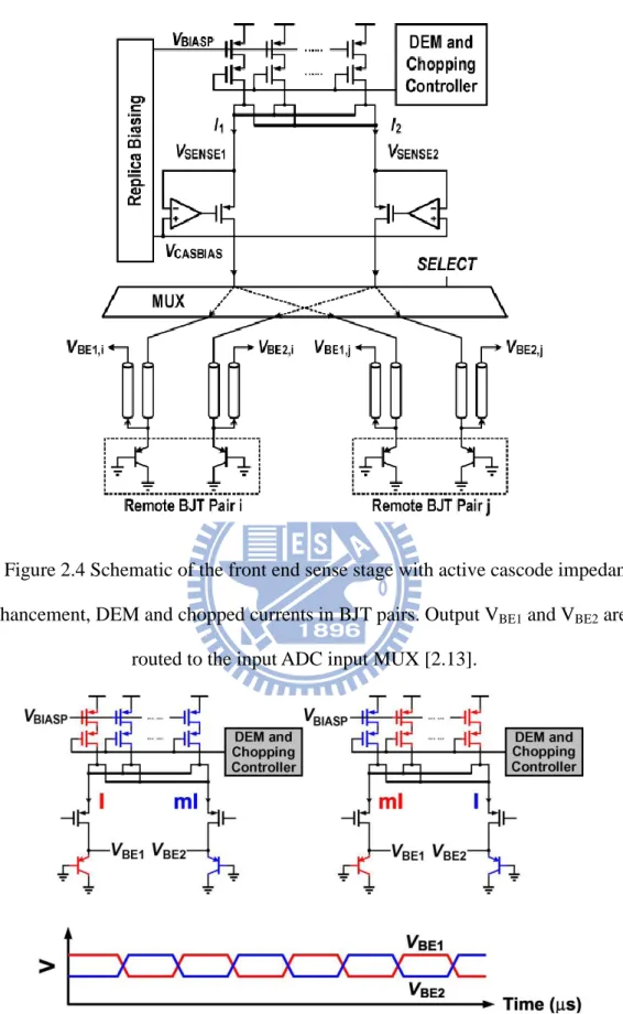
Figure 2.3 Schematic of the thermal sensing system [2.13].
Figure 2.4 shows the simplified schematic of the BJT sense stage. The top-row current sources feed currents in to a pair of matched BJTs to develop a differential voltage. The current ratio, m, between the BJTs results in a differential voltage. In practice, the BJT performance changes with current density. At low current density generation-recombination dominates the BJT behavior while at high current density high-injection dominates. A region of optimal current density (flat- β) is selected to ensure BJTs have comparable β at both current ratios. In this work, the bias current of a single current source is nominally 80 uA. The current is generated using constant-gm bias circuit that uses an nMOS transistor in linear region as a resistive reference. Different current densities can be realized by current, or the BJT emitter area scaling, or both. In this work current scaling was selected as different emitter areas cannot be matched perfectly owing to interconnect-dominated mismatch as the mismatch is dominated by the interconnect. The effective emitter resistance in each BJT branch will
12
be different due to differences in the routing resistance connecting the constituent BJT elements. Additionally, the variable resistance to each unit BJT produces a non-uniform current in that BJT leading to variations and errors. The use of equal area BJTs allow for a layout with symmetrical metal connections to ensure matched contact resistance.
The input current in each branch is swapped between the BJTs every 128 cycles so that differential output voltage is up-converted to the chopping frequency. The selection of the current sources to chop the currents to the BJTs is illustrated in Figure 2.5. The current ratio in the BJTs must be accurate for a measurement with low variations. Each individual current source must be matched so that an exact ratio can be obtained. Careful attention to layout is necessary to eliminate systematic process induced mismatches; a common centroid layout of the unit transistors is used. A discussion of the random mismatch in a high-k metal gate CMOS process is presented. One way to improve the random mismatch is to use long channel length devices, but is area inefficient. Another way to improve matching is to use a dynamic element matching (DEM) between the current sources. A number of redundant current sources are used to generate the current ratio. In the current scheme NCS, discrete current sources are used to generate the current ratio. A digital controller combines the DEM selection with the chopping logic to connect the current sources to the BJT.
13
Figure 2.4 Schematic of the front end sense stage with active cascode impedance enhancement, DEM and chopped currents in BJT pairs. Output VBE1 and VBE2 are
routed to the input ADC input MUX [2.13].
Figure 2.5 Illustration of the current chopping to up-convert the temperature signal to fchop [2.13].
14
2.3 Analog CMOS Based Temperature Sensor
With the use of bipolar transistors for temperature sensing, and advanced techniques including chopping circuit, dynamic element matching and sigma-delta ADC for noise suppression and cancellation, Pertijs et al. [2.5] developed an on-chip temperature sensor with a 3σ inaccuracy of ±1˚C at the expense of increased circuit complexity. With the use of three CMOS transistors for temperature sensor was presented in [2.17]. The three-transistor temperature sensor shows in Figure 2.6, which utilizes the temperature characteristic of the threshold voltage, shows highly linear characteristics at a power supply voltage of 1.8 V. The conditions of this temperature sensor are defined as follows.
Figure 2.6 Conventional three-transistor temperature sensor [2.17].
1) All transistors operate in the saturation region.
2) The output voltages of each node are equal.
3) The sinking currents at each node are equal.
The temperature is obtained by measuring VOUT, where the two currents, IOUT1 and IOUT2, have the same value. When the substrate bias effect of the transistor M2 is
15
neglected to simplify the calculation, their IDS-VGS characteristics and the operating conditions are 2 1 1 1 1 ( ) 2 GS T DS V V I (2.2) 1 1 1 1 L W COX eff (2.3) 2 2 2 2 2 ( ) 2 GS T DS V V I
(2.4) 2 2 2 2 L W COX eff (2.5) 2 3 3 3 3 ( ) 2 GS T DS V V I
(2.6) 3 3 3 3 L W COX ef (2.7) 3 2 1 DS DS DS I I I (2.8) 1 1 GS OUT V V ,VOUT2 VGS2 VGS3 (2.9) 2 1 OUT OUT V V (2.10)After solving (2.3) - (2.6) for each transistor‘s respective VGS, the results are applied to VGS2and VGS3 in (2.8). Then, IDS2 and IDS3 are also substituted for (2.1) & (2.2) using (2.7). Finally, (2.9) is solved against VGS1 and we get
T V V V V VOUT GS T T T ) / / ( 1 ) / / ( 3 1 2 1 1 3 1 2 1 3 2 1 1
(2.11) dT dV b dT dV dT dV a dT dVOUT1 T2 T3 T1 ) ( (2.12)16 Where ) / / ( 1 1 3 1 2 1 a , 1 ( / / ) / / 3 1 2 1 3 1 2 1 b
Since 1/2 1/3 can be assumed as constant, the variables and in (2.12) also become constant. Therefore, the output voltage corresponds to the temperature coefficients of the transistor threshold voltages.
Figure 2.7 Conventional three-transistor temperature sensor [2.17].
Figure 2.7 shows the characteristics at 1.8V and 1V supply voltages, where the intersections of and correspond to the operating points of this sensor. This method shows highly linear characteristics at a power supply voltage of 1.8V or more, which enables us to define the operating conditions well above twice the threshold voltage. But the linearity diminishes after scaling down the supply voltage to 1V using a 90-nm CMOS process. Because the temperature coefficient of the operating point‘s current at a 1V supply voltage is steeper than the coefficient at a 1.8V supply voltage, the operating point‘s current at high temperature becomes quite small and the output
17
voltage goes into the sub-threshold region or the cutoff region.
To improve linearity at a 1V supply voltage, an accurate four-transistor temperature sensor was designed in [2.18], and developed for thermal testing and monitoring circuits in deep submicron technologies, which is shown in Figure 2.8. Note that to operate the additional transistor in the saturation region, an extra bias voltage VGS0‘ is required. Of course, the bias voltage generation circuit must not possess temperature dependency, and, in some cases, this circuit becomes larger than the temperature sensor itself.
Figure 2.8 Four-transistor, voltage output, temperature sensor [2.18].
In addition, the W/L ratio of the transistors M0‘ and M1‘ should be as small as possible so that the current IOUT1‘ remains small. However, the smaller W/L ratio requires a longer channel, so it occupies larger chip area. Consequently, there is a tradeoff between the current consumption and the chip area.
The IDS VGS characteristics and the operating conditions of both the proposed four-transistor sensor is the following:
18 T V I V I V T DS T DS OUT 3 3 3 2 2 2 1 2 2 (2.13) 3 3 2 2 2 2 DS DS I
I can be assumed as a constant value. Thus, (2.13) shows that
the output voltage is mainly proportional to the temperature characteristics of the threshold voltage (M2andM3).
The output current of four- transistor temperature sensor is more high linearity with high temperature than conventional three-transistor circuit shows in Figure 2.9.
Figure 2.9 Operating points of four-transistor temperature sensor [2.18].
2.4 Delay Based Temperature Sensors
2.4.1 Time-to-Digital Converter Based Temperature Sensors
The temperature sensor composed of temperature-to-pulse generator and cyclic time-to-digital converter, shows in Figure 2.10. Temperature-to-pulse generator, it can
19
generate a pulse width is linear to temperature variation. A simple circuit utilizing gate delays to generate the thermally sensitive pulse is shown in Figure 2.11. The START signal is delayed a certain amount of time by the delay line composed of even number of inverter. The high-to-low and low-to-high propagation delay time for an inverter can be expressed as [2.19] ) 5 . 0 2 5 . 1 ln( ) ( ) ( 2 2 DD TN DD TN DD N L TN DD N TN L PHL V V V V V K C V V K V C t (2.14) ) 5 . 0 2 5 . 1 ln( ) ( ) ( 2 2 DD TP DD TP DD P L TP DD P TP L PHL V V V V V K C V V K V C t (2.15)
Figure 2.10 Block diagram of the time-to-digital temperature sensor [2.19].
Figure 2.11 Temperature-to-pulse generator [2.19].
Where kN NCOX(W/L)N , kP PCOX(W/L)P and CL are the trans -conductance parameters and effective load capacitance of the inverter. Note that we
20
assume square-law behavior for the CMOS devices and thereby ignore the effects of velocity saturation. For an inverter with equivalent NMOS and PMOS, the propagation delay can be derived as
) 5 . 0 2 5 . 1 ln( ) ( ) / ( 2 DD T DD T DD OX L PHL PLH P V V V V V C C W L t t t (2.16) Where km T T ) ( 0 0
,km
1
.
2
~
2
.
0
(2.17) ) ( ) ( ) (T V T0 T T0 VT T ,
0
.
5
~
3
.
0
mv
/
k
(2.18) As the temperature increases, the mobility (μ) and the threshold voltage (VT) will both decrease. In the case of VDD much larger than VT, the thermal effect of the propagation delay will be dominated by the mobility. That is, the thermal coefficient of the propagation delay will become positive. The major problem of the simple temperature-to-pulse generator is that the width of the output pulse at the lower bound of the measurement range is usually much larger than zero. This will cause a large DC offset at the smart temperature sensor output. The second delay line with thermal compensation for temperature sensitivity reduction is inserted in the lower transmission path of the START signal to reduce the width offset of the output pulse, which is shown in Figure 2.12. The width offset of the output can be easily reduced by adjusting the number of delay cells in delay line 2.21
Figure 2.12 Width offset reduction accomplished by delay line 2 [2.19].
As shown in Figure 2.13, a simple thermal compensation circuit is used to reduce the sensitivity of the inverter in delay line2. The diode connected transistors P1, N1, and P3 serve as the core of the thermal compensation circuit. Since P1, P3, and N1 are all diode connected, they will operate in saturation if bias current is flowing. Thus, we have
Figure 2.13 Operating points of four-transistor temperature sensor [2.19].
)
1
(
)
)(
(
2
1
3 2 3 3 OX GSP T GSP DPV
V
V
L
W
C
I
(2.19)22
( ) ( )
(1 ) ) )( ( 2 1 3 2 0 0 3 0 0 3 GSP T GSP km OX DP V V T T T V T T L W C I (2.20)When the temperature is higher than 200K, a significant plateau effect can be observed for the difference between mask channel length and effective channel length. The thermal sensitivity of channel length modulation term (1
VGSP3)will be neglected in the following deviations since it is much smaller than those of mobility and threshold voltage over the temperature range we are interested.To get the minimum thermal sensitivity, let 3 0
T IDP
( ) ( )
(1 ) ) )( ( ) 1 ( ) ( ) ( ) )( ( 2 3 0 0 3 0 0 3 2 0 0 3 1 0 0 0 GSP T GSP km OX GSP T GSP km OX V T T T V V T T L W C V T T T V V T T L W T km C After simplification, we have
km
T
T
T
T
V
V
GSP3
T(
0)
(
0)
2
(2.21)The sizes of transistors P1 and N1 are adjusted to make the gate-to-source voltage of P3 fit the requirement stated in (2.21) as closely as possible. The conduction current of transistor P3 can be found by substituting (2.21) back into (2.20) to yield
) 1 ( 2 ) )( ( 2 1 3 2 0 0 3 GSP km OX DP V km T T T L W C I (2.22)
When
km
2
, the drain current will become totally thermal independent) 1 ( ) )( ( 2 1 3 2 0 0 3 OX GSP DP T V L W C I
23
the inverter will be kept thermally insensitive as well, as will the propagation delay of delay line 2. This greatly reduces the design difficulty and enhances the tolerance to process variation.
For accuracy enhancement, a novel time-domain SAR smart temperature sensor suitable for curvature compensation is proposed in [2.20]. The corresponding architecture is shown in Figure 2.14 which evolves from the former time-domain digital thermostat [2.21]. A SAR control logic is added to speed up the set-point programming of the thermostat for adjusting the ARDL delay to approximate the TDDL delay. The final set-point value is defined as the output of the proposed sensor.
Figure 2.14 Implemented architecture of the proposed smart temperature sensor [2.21].
More specifically, the SAR control logic, ARDL and time comparator can be viewed as an equivalent time-to-digital converter to measure the TDDL delay for any temperature under test. The accuracy enhancement is accomplished mainly by a new
24
technique called curvature compensation by which the curvature of ARDL temperature-to-time transfer curve is designed to compensate for TDDL curvature to substantially improve the sensor‘s linearity.
From (2.15),(2.16) and (2.17), (2.15) can be rewritten as
(2.23) where the constant β is almost temperature-independent. Although the unit reference delay of ARDL can be easily implemented as one reference clock period, or a part of it, to be theoretically temperature-insensitive, the curvature of the smart sensor output will inevitably resemble that of curve and the sensor accuracy will be seriously limited as predicted in Figure 2. 15(a). One feasible linearization technique for the smart sensor output is to compensate for the curvature of TDDL curve by that of ARDL curve, as revealed in Figure 2. 15(b).
Figure 2. 15 Sensor output linearity for (a) temperature-insensitive and (b) curvature -compensating ARDL cell delay [2.21].
To reduce the thermal sensitivity of the ARDL delay cell to make its delay as a unit time reference, the temperature compensation circuit adopted in the former
25
time-domain sensor [2.19] is utilized likewise. However, the conventional temperature compensation circuit consumes continuous power. NMOS switch NS1 is added to shut down the quiescent current of the ARDL delay cell between measurements to reduce power consumption as shown in Figure 2.16 where the Stop signal is activated at the end of conversion. The other switch NS2 is inserted to match the source resistances of N1 and N2 for reducing current mirror error. To cut the delay line size and the conversion time in half, the ARDL delay cell can be theoretically implemented as a temperature-compensated NOT gate instead of a delay buffer [2.10]. In this case, however, the rise time and fall time of the NOT gate are not equal since the pull up current is usually not the same as the pull down current. This mismatch will cause additional errors between even and odd stages. Therefore, a thermally compensated buffer is used instead as the unit ARDL delay cell.
Figure 2.16 Modified temperature compensation circuit for the ARDL delay cell [2.21].
26
2.4.2 Dual-DLL-Based All-Digital Temperature Sensor
With process scaling down continuously, PVT variation will be a big problem about Time-to-digital based temperature sensors. A new type DLL-based all-digital temperature sensor [2.22] was presented. It has two improvements. First, it removes the effect of process variation on inverter delays via calibration at one temperature point, thus, reducing high volume production cost. Second, we used two fine-precision DLLs, one to synthesize a set of temperature-independent delay references in a closed loop, the other as a TDC to compare temperature-dependent inverter delays to the references. The use of DLLs simplifies sensor operation and yields a high measurement bandwidth (5kS/s) at 7bit resolution, which could enable fast temperature tracking.
We execute calibration and delay normalization using the circuit of Figure 2.17. It contains an open-loop delay line, and a DLL that synthesizes temperature -independent-delay references. This reference-DLL (R-DLL) is locked to a crystal oscillator x(t): each delay cell in the R-DLL has constant delay Δ0. MUX-1 taps a node in the R-DLL delay line: if the N-th cell‘s output is tapped, the delay from input x(t) to output d(t) of the R-DLL is DDLL = NΔ0. This is our delay reference independent of temperature and process. N can be altered to produce different reference delays. In the open-loop line, if the M-th cell‘s output is tapped by MUX-2, the delay between input x(t) and output c(t) is varies with temperature and process.
27 MUX-2 (M) D Q MUX-1 (N) y(t) FSM Charge pump PD x(t) Stable clock Control voltage Open loop delay line
Reference DLL (R-DLL) ∆0
Figure 2.17 Basic architecture of DLL-based CMOS digital temperature sensor [2.22].
In calibration mode at temperature TC, we set N = NC to fix the reference delay at DDLL = NCΔ0. We then increase M (MUX-2 setting) until DOL equals DDLL at M = MC. This comparison of DOL to DDLL to find their lock at M = MC is done via the bang-bang phase detector in the middle of Figure 2.18. Then the MC value is corresponding to process corner.
Once 1-point calibration is complete, the sensor enters measurement mode. Temperature T is unknown, thus, DOL of the hardwired open-loop line is an unknown delay, which the M-DLL measures by varying the reference delay DDLL of the R-DLL (bottom of Figure 2.18). MUX-1 setting N is varied until DDLL equals DOL at N = Nm. Nm is a digital output that faithfully represents T. Nm corresponds to the normalized delay seen earlier.
28 D Q y(t) FSM x(t) Stable clock Open-loop Delay line (M) R-DLL (N=NC) c(t) d(t) M control (MUX-2) Fixed delay DDLL=NC∆0 Calibration Mode D Q y(t) FSM x(t) Stable clock Open-loop Delay line (M) R-DLL (N=NC) c(t) d(t) N control (MUX-1) DOL at an unknown T Measurment Mode X(t) d(t) M=1 y(t) M=2 M=3 M=MC t X(t) c(t) N=1 y(t) N=2 N=3 N=Nm t DDLL=NC∆0 Fixed delay DOL at an unknown T
Figure 2.18 Calibration mode (top) and measurement mode (bottom) [2.22].
2.4.3 Sub-μW Embedded CMOS Temperature Sensor
In [2.23], An ultra-low power embedded CMOS temperature sensor based on serially connected sub-threshold MOS operation is implemented in a 0.18 μm CMOS process for passive RFID food monitoring applications. Employing serially connected sub-threshold MOS as sensing element enables reduced minimum supply voltage for further power reduction, which is of utmost importance in passive RFID applications. Both proportional-to-absolute-temperature (PTAT) and complimentary-to-absolute- temperature (CTAT) signals can be obtained through proper transistor sizing. With the sensor core working under 0.5 V and digital interfacing under 1 V, the sensor dissipates
29
a measured total power of 119 nW at 333 samples/s and achieves an inaccuracy of ±1/ 0.8 C from 10 C to 30 C after calibration. The sensor is embedded inside the fabricated passive UHF RFID tag. Measurement of the sensor performance at the system level is also carried out, illustrating proper sensing operation for passive RFID applications.
Figure 2.19 shows the block diagram of the proposed temperature sensor in the RFID tag. The proposed temperature sensor first generates and the signals from the sensor core utilizing MOS devices operating in sub-threshold region. These signals are converted to delays through the corresponding delay generators. The resultant temperature modulated output pulse PW, which is level-shifted to 1 V swing for interfacing at the output of the delay generators, is further digitized using the clock signal. This time-domain readout scheme eliminates the use of power hungry ADC to reduce power consumption. For system level implementation, the sensor reuses the existing supply voltages and clock signals available in the tag to reduce the power and area overhead. The sensor supply voltages, VDDL =0.5V and VDDH =1V, are provided by the on-chip power management unit. The supply voltages are provided by LDOs with filtering to reduce both noise at the RF frequency and the ripple voltage, as required by the sensor and other building blocks to ensure robust tag operation. The clock generator generates the system clock, and this clock is utilized by the sensor for quantization. This quantization clock is generated through injection locking. In that case, its frequency is referenced to the incident RF input and should be weakly dependent to both process and temperature variation. The sensor control signals are generated and the digitized temperature data received by the digital baseband. In order to further reduce power consumption, a Done signal is exerted at the end of each conversion period to shut-down the analog building blocks and to acknowledge the baseband. The
30
digital data Dout is then ready and can be read out.
Figure 2.19 Block diagram of the proposed temperature sensor with interfacing in the RFID tag system [2.23].
Figure 2.19 illustrates the PTAT and CTAT delay generators that convert the temperature modulated signal from voltage domain to time domain for simple and power efficient processing. Without loss of generality, we first consider the CTAT delay generator. Transistors MP7-8, together with the resistor RPT and the amplifier, convert the input voltage into VPTAT current IPTAT. Low-voltage operation is sustained by implementing the amplifier using simple current mirror architecture. Stacking of transistors is avoided by having the amplifier output directly driving. The scaled current from is mirrored through MP9-10. Transistors MP10-15 operate as a single-slope ADC, which also performs level-shifting from 0.5 V to 1 V for interfacing with other digital
31
circuits. Similarly, the PTAT delay generator converts VCTAT into ICTAT, followed by another single-slope ADC. At the start of each integration cycle, the VST signal is exerted, shutting down MP11 (MC11). The temperature modulated current signals (which is converted from VPTAT or VCTAT) is integrated through capacitor CPT (CCT). Upon reaching the switching threshold of MP12-13 (MC12-13), a rising edge is triggered and buffered by MP14-15 (MC14-15).As the discharging currents are temperature dependent, the delay between the two rising edges is also temperature dependent. The two rising edge signals from the CTAT and PTAT delay paths are XORed to generate a temperature modulated pulse width PW (Figure 2.21) and then further quantized using the ripple counter and the system clock. The whole block is shut-down through the feedback signal (refer to Figure 2.19), which also indicates the end of conversion.
Figure 2.20 Block diagram of the proposed temperature sensor with interfacing in the RFID tag system [2.23].
32
Figure 2.21 Simulated temperature modulated pulse width from -10 ˚C to 30 ˚C [2.23].
2.5 Leakage Based Temperature Sensor
The amazing integration densities achieved by current submicron technologies pay the price of increasing static power dissipation with the corresponding rise in heat density. Dynamic Thermal Management (DTM) techniques provide thermal-efficient solutions to balance or equally distribute possible on-chip hot spots. Accurate sensing of on-chip temperature is required by optimally allocating smart temperature sensors in the silicon. [2.24] introduce an ultra low-power (1.05–65.5nW at 5 samples/s) tiny (10250 μm2) CMOS smart temperature sensor based on the thermal dependency of the leakage current. The proposed sensor outperforms all previous works, as far as area and power consumption are concerned (more than 85% reduction in both cases), while still
33
meeting the accuracy constraints imposed by target application domains. Furthermore, a specific interface based on the use of a logarithmic counter has been implemented to digitalize the temperature sensing. These facts, in conjunction with the full compatibility of the sensor with standard CMOS processes, allow the easy integration of many of these tiny sensors in any VLSI layout, making them specially suitable for modern DTM implementations.
The structure of the sensor is displayed in Figure 2.22. Similarly to what happens in dynamic gates, when the input receives a low-to-high transition and transistor M1 goes from an “on” to an “off” condition, capacitor CL stores a charge that
ideally would remain untouched, but that actually will gradually leak away due to leakage currents.
Figure 2.23 shows the sources of leakage for transistors M1 and M2. Sources (1) and (2) are sub-threshold leakages of M2 and M1, respectively. As mentioned before, these two components will dominate the behavior of the sensor. Sources (3) and (4) are reverse-biased diode leakages of M2 and M1, respectively. Sources (1) and (3) discharge CL, whereas sources (2) and (4) charge it. When CL is charged, the transistor
M2 drain-source voltage (VDS,M2) equals VDD and its sub-threshold current (IDSUB,M2)
34
Figure 2.22 Sub-threshold current thermal sensor [2.24].
Figure 2.23 Leakage current mechanisms in the thermal sensor [2.24].
Figure 2.24 shows the implementation of the sensor along with the logarithmic counter. A clock—clock_in—drives the input of the sensor, after charging with a narrow low pulse, its low-to-high transition leaves the intermediate node floating and sets when the logarithmic count must start. When, due to the leakage process, crosses the threshold voltage of inverter M3-M4, the logarithmic counter receives a low-to-high transition at the load input, the count ends and is registered. Note that the loading rate of the register, i.e., the conversion rate of the sensor, is equal to the frequency of clock_in. This frequency is bounded by the pulse width of the minimum temperature that the sensor needs to measure. An external control will decide this conversion rate depending on the precision and power requirements of the system.
35
Figure 2.24 Implementation of the sensor along with the logarithmic counter [2.24].
2.6 Frequency-to-Digital Converter Based Temperature
Sensor
The temperature sensor proposed by [2.25] is operating with the FDC and the controller as shown in Figure 2.25. Temperature is measured by the frequency difference between the temperature sensitive oscillator (TSO) and the temperature insensitive oscillator (TIO). Digital output consisting of 10b coarse and 3b fine binary codes are extracted from the FDC. In order to reduce power consumption, the TIO and the TSO operate alternatively depending on the signals sent by the controller, S1 and S2, which are also used to synchronize both oscillators. Controlling signals have enough margins to account for the settling time of both oscillators, which is necessary for switching them. The difference of the frequencies between the TSO and the TIO is used to measure temperature. Consequently, the countable temperature range at a given the number of bits can be increased as shown in Figure 2.26. The frequency variation due to process variation can also be canceled.
36
Figure 2.25 Block diagram of the temperature sensor proposed [2.25].
Figure 2.26 Enhanced performance of temperature measurement with the TIO [2.25].
Both of the TSO and TIO are constructed from ring oscillators using a current starved delay cell shown in Figure 2.27. However, the temperature insensitive bias circuit is adopted only in the TIO. The TSO has the frequency range of 400MHz (at -40°C) ~ 250MHz (at 110°C), which has linear relation to the temperature variation. The TIO, whose mean frequency is 200MHz, can serve as the reference for the TSO.
Figure 2.28 shows the block diagram of the FDC which consists of a 10b up-down counter, a sampler, and the fine code generator (FCG) and shows the timing diagram.
37
When Up- Down is high, the MUX selects the TSO output as the FDC‘s input clock. The counter then counts rising edges of the input clock upward. Conversely, when Up-Down is low, the MUX selects the TIO output as the FDC‘s input clock. The counter then counts the rising edges of the input clock downward. Therefore, the sampler can register the frequency difference between the TSO and the TIO with S3. For the next measurement, S4 resets the counter, which completes one temperature-to-digital conversion. One period of Up-Down is the same as one conversion time. In order to prevent an overflow and to maximize the capability of the counter, the frequency of Up-Down should be as in (2.24).
38
Figure 2.28 (a) Block diagram of a FDC and (b) timing diagram of the control signal [2.25].
2.7 Summary
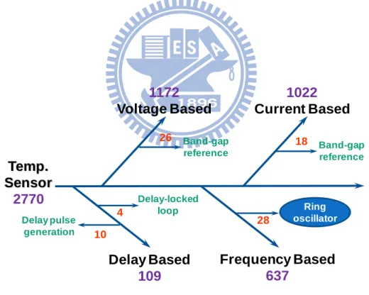
Figure 2.29 shows the fishbone diagram of temperature sensor patents (US patents). There are 2770 search results in term of temperature sensor, BJT based and analog CMOS based temperature sensors belonging to the majority. These two type temperature sensors utilize BJT bias and band-gap reference to sense temperature variation. TDC based and FDC based temperature sensors are in the minority, utilizing inverter chain and ring oscillator to generate time pulse and frequency linearly with temperature. Figure 2.30 and Table2.1 compare several temperature sensors in previous
39
section. As the conversion speed goes up, the more current is needed. Therefore the power consumption is compared with respect to the measurement bandwidth. The voltage and current based temperature sensors [2.4], [2.5], [2.14]-[2.16] have large power consumption per conversion rate and low area efficiency because they make use of ADCs. Power consumption per conversion rate of TDC based temperature sensors, [2.19]-[2.21], are lower than previous one, but the delay chain occupies large area. [2.23] have less power consumption but smaller sensing range (-10˚C~30˚C) which is suitable for RFID. [2.24] has extreme low power because slow conversion rate, but it‘s effected significantly by process variation. While consuming the lowest power per conversion rate, the FDC based temperature sensor [2.25] shows moderate resolution.
Ring oscillator 1172 Voltage Based Delay-locked loop Temp. Sensor 2770 Delay Based 109 26 Frequency Based 637 4 28 10 Delay pulse generation Band-gap reference 1022 Current Based 18 Band-gap reference
40 ▲ Pertijs, JSSC, 2005 [2.5] 3.3V, ±0.1°C, 0~100°C, 0.01°C ▲ Aita, ISSCC, 2009 [2.4] 3.3V, ±0.1°C, -55~125°C, 0.025°C ▲ Vroonhoven, ISSCC, 2008 [2.16] 5V, ±0.05°C, -55~125°C, 0.025°C ▲ Chen, JSSC, 2005 [2.19] 3.3V, -0.7~+0.9°C, 0~100°C, 0.16°C ▲ Chen, JSSC, 2010 [2.21] 3.3V, -0.25~+0.35°C, 0~90°C, 0.092°C ▲ Woo, ISSCC, 2009 [2.22] 1.2V, -1.8~+2.3°C, 0~100°C, 0.66°C ▲ Kim, CICC, 2009 [2.25] 1.2V, -2.9~+2.75°C, -40~110°C, 0.043°C ▲ Li, ISSCC, 2009 [2.14] 1.05V, ±5°C, -10~110°C, 0.45°C
* Supply, Inaccuracy, Range, Resolution 1E-5 1E-4 1E-3 1E-2 1E-1 1E+0 1E+1 1E+2 0 1 2 3 4
Power Consumption per
Conversion Rate (μW/samples/sec)
102 101 100 10-1 10-2 10-3 10-4 10-5 Pertijs Aita Vroonhoven Chen, 2005 Chen, 2010 Woo Kim Li 32nm 65nm 0.13μm 0.35μm 0.7μm Technology Node (μm) 5E-4 5E-3 5E-2 5E-1 5E+0 0 1 2 3 4 Area (mm 2 ) 5x100 5x10⁻¹ 5x10⁻² 5x10⁻³ 5x10⁻⁴ Pertijs, Aita Vroonhoven Chen, 2005 Chen, 2010 Woo Kim Li 32nm 65nm 0.13μm 0.35μm 0.7μm Technology Node (μm)
Figure 2.30 Comparison of temperature sensors.
Table 2.1 Comparison of each type temperature sensors.
Type Paper Advantage Disadvantage
BJT Based
[2.5],[2.14] -[2.16]
High resolution and small inaccuracy.
Large area and large power. Can‘t be operated in low voltage.
CMOS Based
[2.17], [2.18]
Better linearity, lower supply voltage and power than BJT-based
Need additional ADC and bias circuits.
Delay Based
[2.19]- [2.23]
Don‘t need additional ADCs, it‘s easier to be implemented.
Large area of delay line. Can‘t be operated in low voltage.
Leakage Based
[2.24] Small power and area. Low conversion rate.
Additional log counter is required. Can‘t be operated in low voltage.
Frequency Based
41
Chapter 3
0.5V~0.25V Process, Voltage and
Temperature Sensors with Adaptive
Voltage Selection
The 0.5V~0.25V process, voltage and temperature (PVT) sensors with adaptive voltage selection are proposed for temperature measurement in the energy harvesting dynamic voltage and frequency scaling (DVFS) systems. It composes of process, voltage and temperature sensor. The process sensor and voltage (PV) sensor monitor the process variation and voltage variation continuously and give the variation information for temperature compensation. The temperature sensor has six TSROs generating frequency proportional to the measurement temperature at suitable supply voltage, and converts the frequency into digital code. The sensor was designed in TSMC 65nm CMOS technology. The sensor operate over an ultra-low voltage range from 0.25V~0.5V and have 2.3μW power consumption, 0.15˚C resolution and 50k samples/sec conversion rate.
3.1 Introduction
In recent years, numerous portable electronic products have been launched to the market with considerable market growth. Energy efficiency of electronic circuits is a critical concern in every application. Lowering the supply voltage and frequency is one
42
of the attractive approaches to reduce power consumption. Furthermore, dynamic voltage and frequency scaling (DVFS) system achieves extremely efficient energy saving by adjusting system supply voltage and frequency depending on workload monitor [3.1]. As we continue to reduce the supply voltage to ultra-low voltage that the transistor reach the near/sub-threshold regions, circuits would become more sensitive to process, voltage and temperature (PVT) variations than super threshold [3.2]-[3.4].
Figure 3.1 The DVFS system of energy harvesting.
With process scaling down continuously, the high level of integration also introduces the problem of self-heating, which is the result of increased power density. The environmental variations are so large that variation-aware near-/sub-threshold circuit design is necessary to prevent functional failure [3.5]. Besides, the energy harvesting systems, which power source include solar, RF and thermo, have critical factor of power efficiency [3.6]-[3.7]. As the result, the power consumption of temperature sensors should be as low as possible to be applicable to the DVFS systems of energy harvesting. As shown in Figure 3.1, the system is constructed by several
![Figure 2.10 Block diagram of the time-to-digital temperature sensor [2.19].](https://thumb-ap.123doks.com/thumbv2/9libinfo/8736814.203315/31.892.161.746.326.985/figure-block-diagram-time-digital-temperature-sensor.webp)
![Figure 2.16 Modified temperature compensation circuit for the ARDL delay cell [2.21]](https://thumb-ap.123doks.com/thumbv2/9libinfo/8736814.203315/37.892.191.656.524.927/figure-modified-temperature-compensation-circuit-ardl-delay-cell.webp)
![Figure 2.17 Basic architecture of DLL-based CMOS digital temperature sensor [2.22].](https://thumb-ap.123doks.com/thumbv2/9libinfo/8736814.203315/39.892.254.644.103.506/figure-basic-architecture-based-cmos-digital-temperature-sensor.webp)
![Figure 2.19 Block diagram of the proposed temperature sensor with interfacing in the RFID tag system [2.23]](https://thumb-ap.123doks.com/thumbv2/9libinfo/8736814.203315/42.892.129.757.162.739/figure-block-diagram-proposed-temperature-sensor-interfacing-rfid.webp)
![Figure 2.20 Block diagram of the proposed temperature sensor with interfacing in the RFID tag system [2.23]](https://thumb-ap.123doks.com/thumbv2/9libinfo/8736814.203315/43.892.134.759.544.1015/figure-block-diagram-proposed-temperature-sensor-interfacing-rfid.webp)
![Figure 2.22 Sub-threshold current thermal sensor [2.24].](https://thumb-ap.123doks.com/thumbv2/9libinfo/8736814.203315/46.892.173.731.122.348/figure-sub-threshold-current-thermal-sensor.webp)
![Figure 2.24 Implementation of the sensor along with the logarithmic counter [2.24].](https://thumb-ap.123doks.com/thumbv2/9libinfo/8736814.203315/47.892.166.733.106.353/figure-implementation-sensor-logarithmic-counter.webp)