適用於視訊應用的智慧型記憶體控制器設計
68
0
0
全文
(2) 適用於視訊應用的智慧型記憶體控制器設計 研究生:蔡旻奇. 指導教授:張添烜 博士. 國立交通大學電子研究所碩士班. 摘. 要. 隨著超大型積體電路製程快速的進步,愈來愈多的元件可以輕易整合進單晶片系 統。對於這些需要高度運算能力的系統來說,記憶體子系統,特別是外部動態隨機存取 記憶體的頻寬跟功率消耗,是一個需要優先評估及最佳化的重點。這對一個晶片是否成 功來說很重要。 在這篇論文中,我們考慮動態隨機存取記憶體的頻寬和功率消耗,以及傳輸等待時 間,然後提出一個智慧型記憶體控制器設計。這個設計是利用我們自製的可設定多媒體 平台模擬器來評估及開發。 對於最複雜的視訊電話模擬設定來說,我們提出幾種技巧來達到高度平均記憶體頻 寬使用率。首先,我們使用記憶體同步定址來提高頻寬使用率同時降低傳輸等待時間。 接著,根據視訊電話傳輸資料的特性,我們提出一種「改良式先到先處理」的排程方法。 這個方法可以增加頻寬使用率同時降低記憶體功率消耗。最後,我們使用「等待時間重 於指令種類」的記憶體指令排程方式來隱藏記憶體運作等待時間。如此,開發出的記憶 體控制器改善平均頻寬使用率從 40%到 72%,並需要約 485 毫瓦的功率消耗。如果我們 以降低記憶體功率消耗為主要考量,在滿足時間的限制條件下,我們提出另外一種設計 可以節省 26%的功率消耗。 我們將提出的技巧實際設計成硬體。在 0.18 微米的互補式金氧半導體製程下,我 們的設計需要 47.6K 個邏輯閘並可達到 166 百萬赫茲的運作頻率。.
(3) Smart Memory Controller Design for Video Applications Student: Min-Chi Tsai. Advisor: Dr. Tian-Sheuan Chang. Department of Electronics Engineering Institute of Electronics National Chiao Tung University. Abstract With the rapid progress of VLSI process, more and more components are easily to be integrated into one System-on-Chip. For such system with high computational power, the memory subsystem, especially the bandwidth and power consumption of external DRAM, is one of major issues that have to be evaluated and optimized first for the chip success. In this thesis, we propose a smart memory controller design which takes DRAM bandwidth, transaction latency, and DRAM power consumption into consideration. This design is developed and evaluated by a configurable multimedia platform simulator. For the most complex video phone scenario, we propose several techniques to achieve high average DRAM bandwidth utilization. First, we adopt the bank-interleaving support to increase the bandwidth utilization while reduce the transaction latency. Second, according to the scenario characteristics, we propose MFIFS (Modified First In First Serve) as the transaction scheduling policy. It can increase bandwidth utilization while reduce DRAM power consumption. Third, we use LTOT (Lasted Time Over Type) as the DRAM command scheduling policy to hide DRAM operation latencies. Thus, the resulted memory controller improves average bandwidth utilization from 40% to 72% with estimated 485 mW DRAM power consumption for the video phone scenario. If the design has to minimize DRAM power consumption while still meet timing constraints, another proposed memory controller can save up to 26% of power. The proposed techniques are implemented into hardware. The implementation uses 0.18 μm CMOS process with 47.6K gates and achieves 166 MHz operating frequency..
(4) 誌. 謝. 這篇論文能夠完成,有兩個最重要的人。首先,我要感謝我的指導教授張添 烜老師,有他的關心與指導,以及在論文寫作及口試準備期間的幫忙,我才能順 利畢業。另外,感謝張彥中學長在研究進行期間的照顧,每當我有疑惑不解時, 學長總是能陪我討論,讓我找到方向。無論是做為學生或是學弟,我總是意見很 多,叛逆性很強,麻煩你們了。 接下來,我要感謝林佑坤、鄭朝鐘學長,以及 427 實驗室的各位,王裕仁、 吳錦木、余國亘、古君偉、廖英澤、林嘉俊、李得瑋、郭子筠及吳秈璟。有你們, 才有我碩士班的回憶。 我還要感謝一個人,在我畢業前出現在我生命中一個重要的人。謝謝妳,小 慧,在我壓力最大的時候幫我加油打氣。 最後,要感謝我的父母讓我沒有後顧之憂可以完成我的碩士學位。爸、媽, 辛苦了,謝謝你們!.
(5) Content CONTENT .............................................................................................................................................. I LIST OF FIGURE ............................................................................................................................... III LIST OF TABLE ................................................................................................................................... V CHAPTER 1. INTRODUCTION .....................................................................................................1. 1.1. BACKGROUND ........................................................................................................................1. 1.2. RELATED WORK .....................................................................................................................1. 1.3. MOTIVATION AND CONTRIBUTION ..........................................................................................3. 1.4. THESIS ORGANIZATION ..........................................................................................................3. CHAPTER 2 2.1. OVERVIEW OF MODERN ON-CHIP BUS AND DRAM ....................................5. ADVANCE MICROCONTROLLER BUS ARCHITECTURE (AMBA) ..............................................5. 2.1.1. AXI Architecture ...............................................................................................................5. 2.1.2. Channel Handshaking ......................................................................................................7. 2.1.3. Transaction Ordering .......................................................................................................9. 2.1.4. Additional Features ..........................................................................................................9. 2.2. MODERN DRAM..................................................................................................................10. 2.2.1. DRAM Basics..................................................................................................................10. 2.2.2. DRAM Operations .......................................................................................................... 11. 2.2.3. DRAM Power Calculation..............................................................................................14. CHAPTER 3. MULTIMEDIA PLATFORM MODELING..........................................................20. 3.1. INTRODUCTION.....................................................................................................................20. 3.2. MULTIMEDIA PLATFORM ......................................................................................................20. 3.3. MASTER MODELING .............................................................................................................22. 3.3.1. ID Generation.................................................................................................................23. 3.3.2. Type and Address Generation .........................................................................................23. 3.3.3. Write Data Generation ...................................................................................................26. 3.4. AXI NETWORK ....................................................................................................................27. 3.5. MEMORY CONTROLLER ........................................................................................................29. 3.5.1. Memory Controller without Bank-interleaving Support .................................................29. 3.5.2. Memory Controller with Bank-interleaving Support ......................................................32. 3.5.3. Transaction Scheduling Policy .......................................................................................33. 3.5.4. Scoring Function ............................................................................................................35. i.
(6) CHAPTER 4. SIMULATION RESULT AND ANALYSIS ...........................................................37. 4.1. INTRODUCTION.....................................................................................................................37. 4.2. SIMULATION ENVIRONMENT SETTING ..................................................................................38. 4.3. SIMULATION RESULT AND ANALYSIS ....................................................................................40. 4.3.1. DRAM Bandwidth Utilization First ................................................................................40. 4.3.2. DRAM Power Consumption First...................................................................................49. CHAPTER 5. HARDWARE IMPLEMENTATION .....................................................................53. 5.1. HARDWARE DESIGN .............................................................................................................53. 5.2. IMPLEMENTATION RESULT ....................................................................................................55. CHAPTER 6. CONCLUSION AND FUTURE WORK................................................................57. REFERENCE .......................................................................................................................................59. ii.
(7) List of figure FIG. 2-1 GENERIC AXI ARCHITECTURE ......................................................................................................6 FIG. 2-2 (A) CHANNEL ARCHITECTURE OF READS (B) CHANNEL ARCHITECTURE OF WRITES.......................7 FIG. 2-3 (A) VALID BEFORE READY (B) READY BEFORE VALID (C) VALID WITH READY .................8 FIG. 2-4 SIMPLIFIED DRAM ARCHITECTURE ...........................................................................................10 FIG. 2-5 SIMPLIFIED DRAM STATE DIAGRAM ..........................................................................................13 FIG. 2-6 PRECHARGE POWER-DOWN AND STANDBY CURRENT [16] ..........................................................16 FIG. 2-7 ACTIVATE CURRENT [16] ............................................................................................................16 FIG. 2-8 WRITE CURRENT [16] .................................................................................................................17 FIG. 2-9 READ CURRENT WITH I/O POWER [16]........................................................................................18 FIG. 3-1 GENERIC MULTIMEDIA SOC PLATFORM ......................................................................................21 FIG. 3-2 MULTIMEDIA PLATFORM SIMULATOR BLOCK DIAGRAM ..............................................................22 FIG. 3-3 ID TAG FORMAT ..........................................................................................................................23 FIG. 3-4 (A) 1-D ADDRESS TYPE (B) 2-D ADDRESS TYPE (C) CONSTRAINT RANDOM ADDRESS TYPE .........25 FIG. 3-5 A SIMPLE TRANSACTION GENERATION EXAMPLE ........................................................................25 FIG. 3-6 WRITE DATA FORMAT..................................................................................................................26 FIG. 3-7 FIXED PRIORITY ARBITRATION SCHEME ......................................................................................27 FIG. 3-8 ROUND-ROBIN ARBITRATION SCHEME ........................................................................................28 FIG. 3-9 BLOCK DIAGRAM OF THE MEMORY CONTROLLER WITHOUT BANK-INTERLEAVING SUPPORT .......29 FIG. 3-10 BANK STATE TRANSITION AND RELATED COMMANDS WHEN (A) CURRENT BANK STATE IS IDLE (B) CURRENT BANK STATE IS ACTIVE WITH ROW HIT (C) CURRENT BANK STATE IS ACTIVE WITH ROW MISS ...............................................................................................................................................30. FIG. 3-11 BLOCK DIAGRAM OF THE MEMORY CONTROLLER WITH BANK-INTERLEAVING SUPPORT ............32 FIG. 3-12 EXAMPLES OF (A) FIRST IN FIRST SERVE (FIFS) POLICY (B) TWO LEVEL ROUND-ROBIN (TLRR) POLICY (C) MODIFIED FIRST IN FIRST SERVE (MFIFS) POLICY ........................................................34. FIG. 4-1 MEMORY MAPPING OF THE VIDEO PHONE SCENARIO...................................................................39 FIG. 4-2 AVERAGE DRAM BANDWIDTH UTILIZATION WITH FIXED PRIORITY BUS ARBITRATION SCHEME .41 FIG. 4-3 AVERAGE DRAM BANDWIDTH UTILIZATION WITH ROUND-ROBIN BUS ARBITRATION SCHEME ...42 FIG. 4-4 AVERAGE DRAM BANDWIDTH UTILIZATION WITH DIFFERENT SCORING FUNCTIONS ..................43 FIG. 4-5 AVERAGE DRAM BANDWIDTH UTILIZATION WITH DIFFERENT TRANSACTION SCHEDULING POLICIES ........................................................................................................................................45. FIG. 4-6 AVERAGE DRAM BANDWIDTH UTILIZATION WITH DIFFERENT BUFFER SIZES AND THRESHOLDS 46 FIG. 4-7 AVERAGE TRANSACTION LATENCY WITH DIFFERENT BUFFER SIZES AND THRESHOLDS ................47 FIG. 4-8 AVERAGE DRAM POWER CONSUMPTION WITH DIFFERENT BUFFER SIZES AND THRESHOLDS ......47 FIG. 4-9 AVERAGE DRAM BANDWIDTH UTILIZATION TRANSITION THROUGH THE SIMULATIONS .............48. iii.
(8) FIG. 4-10 AVERAGE TRANSACTION LATENCY TRANSITION THROUGH THE SIMULATIONS...........................48 FIG. 4-11 AVERAGE DRAM POWER CONSUMPTION TRANSITION THROUGH THE SIMULATIONS .................49 FIG. 4-12 AVERAGE DRAM POWER CONSUMPTION WITH DIFFERENT OPTIMIZATION POLICIES .................51 FIG. 5-1 HARDWARE BLOCK DIAGRAM OF THE MEMORY CONTROLLER ....................................................53 FIG. 5-2 BLOCK DIAGRAM OF TRANSACTION REORDER UNIT....................................................................54. iv.
(9) List of table TABLE 2-1 KEY DDR SDRAM TIMINGS..................................................................................................14 TABLE 2-2 IDD SPECIFICATIONS USED IN POWER CONSUMPTION CALCULATION ........................................15 TABLE 2-3 PARAMETERS DEFINED FOR EQUATIONS .................................................................................15 TABLE 4-1 EXAMPLES OF SCENARIOS WHICH CAN BE APPLIED TO THE MULTIMEDIA PLATFORM SIMULATOR ......................................................................................................................................................37 TABLE 4-2 TASKS AND THE CORRESPONDING ACCESS PATTERNS OF THE VIDEO PHONE SCENARIO ...........39 TABLE 4-3 BANDWIDTH REQUIREMENT AND TIMING CONSTRAINT OF THE VIDEO PHONE SCENARIO ........39 TABLE 4-4 CONFIGURATION OF THE SIMULATOR IN SIMULATION 1 ..........................................................40 TABLE 4-5 TIMING CONSTRAINT STATUS WHEN FIXED PRIORITY BUS ARBITRATION SCHEME IS APPLIED ..40 TABLE 4-6 TIMING CONSTRAINT STATUS WHEN ROUND-ROBIN BUS ARBITRATION SCHEME IS APPLIED ....41 TABLE 4-7 CONFIGURATION OF THE SIMULATOR IN SIMULATION 2 ..........................................................43 TABLE 4-8 CONFIGURATION OF THE SIMULATOR IN SIMULATION 3 ..........................................................44 TABLE 4-9 CONFIGURATION OF THE SIMULATOR IN SIMULATION 4 ..........................................................45 TABLE 4-10 AVERAGE DRAM BANDWIDTH UTILIZATION AND POWER CONSUMPTION WITH DIFFERENT BUS ARBITRATION SCHEMES ...........................................................................................................51. TABLE 5-1 IMPLEMENTATION RESULT AND COMPARISON .........................................................................55. v.
(10) Chapter 1 Introduction 1.1 Background In recent years, due to explosive improvement in semiconductor technology, the embedded system gets sufficient computing power to implement various consumer electric products and is small enough to fit in a chip. Also, due to great progress in VLSI design methods and the related CAD tools, it takes less and less time to finish a design. Thus, designers feel much more time-to-market pressure. To meet these trends, the concept of SoC and IP is proposed [1]. With a standard on-chip bus, the compliant IPs can be easily integrated to perform SoC. However, IPs are not jigsaw. Before integration, careful evaluation and modification in system level to meet all constraints is necessary [1][2]. The performance and power consumption of external memory is especially critical that have to be evaluated and optimized first. As DRAM advances, data rate is no longer the most critical issue. Instead, its large power consumption in the embedded system becomes a major problem, especially in a portable device [3]. Thus, how to develop a memory controller with balanced DRAM performance and power consumption is important nowadays.. 1.2 Related Work According to DRAM operating characteristics, various scheduling policies are proposed for DRAM performance or power consumption optimization. Scott Rixner’s memory controller reorders DRAM accesses among different streams and within a single stream to optimize the bandwidth utilization [4]. However, since the reordered transactions cannot be sent out of order, they have to be reordered again. Thus, extra hardware cost is required.. 1.
(11) Victor Delaluz proposes several threshold-based policies to turn DRAM into low power state during the interval with no access [5]. Since it is impossible to know when the next access will occur, the return latency from low power state to normal state is the prediction miss penalty. Yongsoo Joo introduces a precise energy characterization of DRAM memory system and explores the amount of energy associated with design parameters. After that, a practical mode control scheme is proposed for the DRAM device [6]. Ning-Yaun Ker not only controls DRAM power states by the threshold-based policy but also by monitoring the DRAM bus utilization to efficiently reduce the prediction miss penalty [7]. However, it doesn’t work when there are sustained accesses. Artur Burchard presents a real-time streaming memory controller with PCI Express interface [8]. Also, he shows both power and latency trade-offs with buffer size. Kun-Bin Lee proposes an efficient quality-aware memory controller for multimedia platform SoC [9]. It utilizes a quality-aware scheduler to provide quality-of-service (QoS) guarantees including minimum access latencies and fine-grained bandwidth allocation. Sonics Limited develops MemMax 2.0 memory controller which improves efficiency of DRAM by up to 40% and also provides QoS guarantees. However, it must be used on Sonics’s own MicroNetwork on-chip bus standard [10]. ARM Limited provides a configurable AXI compliant soft IP, PL340, for the customers [11]. It supports both SDRAM and DDR SDRAM. By utilizing AXI features, it provides exclusive access semaphore support for multiprocessing systems. Moreover, it also supports programmable arbitration with advanced memory access scheduling and QoS for low latency access to memory. However, the design architecture and performance information is limited. The researches about memory scheduling policies listed above have three common defects. First, they address only on DRAM performance improvement or DRAM power consumption reduction. However, the two factors are trade-off and should be evaluated together. Second, they rarely use popular on-chip bus standard. 2.
(12) Hence, the results are hard to compare and may not be so efficient in real applications. Third, only DRAM bandwidth utilization and transaction latency are used to evaluate the performance. Nevertheless, how to make sure all system tasks are done within preset timing constraints is also important from the system viewpoint.. 1.3 Motivation and Contribution The aforementioned issues motivate us to develop an evaluation platform for both DRAM performance and power consumption and a suitable memory controller for the platform. The contribution of this thesis includes the following. 1) The multimedia platform simulator can be easily configured to perform various scenarios for both DRAM performance and power consumption evaluation. 2) The memory controller in the simulator can be easily modified to perform different policies for evaluation before hardware implementation. 3) Propose a method to balance the DRAM performance with different system bus arbitration schemes.. 1.4 Thesis Organization In Chapter 2, the characteristics of modern on-chip bus and DRAM are introduced. Chapter 3 presents our multimedia platform simulator and the memory controller scheduling policies implemented. Then, in Chapter 4, we show the simulation result and analysis. Chapter 5 implements a memory controller according to the simulation result of Chapter 4. Chapter 6 is the conclusion and future work.. 3.
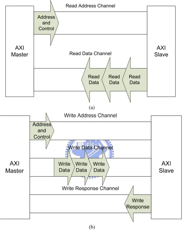
(13) Chapter 2 Overview of Modern On-chip Bus and DRAM This chapter is divided into two parts to introduce modern on-chip bus and DRAM. In Section 2.1, a modern on-chip bus specification is presented. After that, in Section 2.2, we introduce the DRAM basics and how to measure DRAM power consumption in system level.. 2.1 Advance Microcontroller Bus Architecture (AMBA) The AMBA protocol [12] is an open standard, on-chip bus specification which is drawn up by ARM Limited. It is the most popular on-chip bus standard in the world now. The latest version of AMBA is 3.0. It is also called Advanced eXtensible Interface (AXI) [13]. AXI is first brought up in Embedded Professor Forum (EPF), 2003 and its version 1.0 specification is then announced in March, 2004. The most distinct feature of AXI is the out-of-order transaction that makes it ideal for the high performance system and relaxes the constraints to the memory controller.. 2.1.1 AXI Architecture Fig. 2-1 shows a generic AXI architecture. There are five independent channels in charge of communication between the master and slave. The five channels are write address channel, read address channel, write data channel, write response channel, and read data channel respectively. Each channel contains a set of forward signals and one feedback signal. The feedback READY signal is used to cooperate with the forward VALID signal to perform channel handshaking for data and control information transfer. Channel handshaking will be stated later.. 5.
(14) Write Address/Control AWREADY. Read Address/Control ARREADY. AXI Master. Write Data. AXI Slave. WREADY. Write Response BREADY. Read Data RREADY. Fig. 2-1 Generic AXI architecture. When the master initiates a read transaction, it sends address and control information to the slave by read address channel. When the slave receives address and control information, it starts to work. After the slave finishes its task, data are sent back to the master via read data channel. The read transaction is not done until the last burst data is accepted by the master. As to a write transaction, the master sends address and control information to the slave by write address channel first. Then, the master provides data required for the slave via write data channel. Finally, after the slave finishes its task, a response is sent back through write response channel. The master checks the response to see if the write transaction succeeds. Fig. 2-2 presents the process of read transactions and write transactions respectively.. 6.
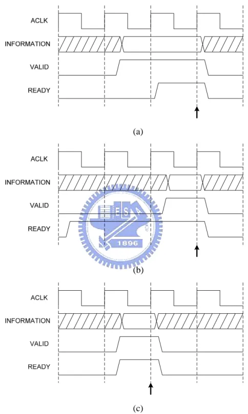
(15) Read Address Channel Address and Control. AXI Master. AXI Slave. Read Data Channel. Read Data. Read Data. Read Data. (a). (b) Fig. 2-2 (a) Channel architecture of reads (b) Channel architecture of writes. 2.1.2 Channel Handshaking All five channels use VALID/READY handshaking to transfer data and control information. This mechanism enables both the master and slave to control transfer rate of data and control information. The source raises the VALID signal to indicate that data or control information is available. The destination raises the READY signal. 7.
(16) to indicate that data or control information can be accepted. Transfer occurs only when VALID and READY signals are both HIGH.. (a). (b). (c) Fig. 2-3 (a) VALID before READY (b) READY before VALID (c) VALID with READY. Fig. 2-3 shows all possible cases in VALID/READY handshaking. Note that the source provides valid data and control information and drives VALID signal HIGH simultaneously. The arrow in Fig. 2-3 indicates when the transfer occurs. 8.
(17) 2.1.3 Transaction Ordering Unlike AMBA 2.0 in which only one granted transaction can use the common system bus interconnect until it is finished, AXI separates channel relations and uses “ID tag” to enable out-of-order transaction completion. Out-of-order transactions improve system performance in two ways: ● Bus interconnect can enable transactions with fast-responding slaves to complete in advance of earlier transactions with slower slaves. ● Complex slaves can return read data out of order. For example, data for a later transaction might be available in internal buffer before data for an earlier transaction is available. Although AXI supports out-of-order transactions, it doesn’t mean that transactions can be reordered at pleasure. The basic rule is “Transactions with same ID tag must be completed in order”. That is, if a master requires transactions to be completed in the same order as they are issued, the master must assert these transactions with the same ID tag. If, however, a master does not require in-order transaction completion, it can supply transactions with different ID tags. The rule stated before is just for the single master system. In a multi-master system, the bus interconnect has to append additional information to the ID tag to ensure that ID tags are unique from all masters.. 2.1.4 Additional Features ●. ●. Burst types AXI supports three different burst types which are suitable for: ¾ Normal memory accesses ¾ Wrapping cache line bursts ¾ Streaming data to peripheral FIFO locations System cache support The cache-support signal of AXI enables a master to provide to a system-level cache the bufferable, cacheable, and allocate attributes of a transaction.. 9.
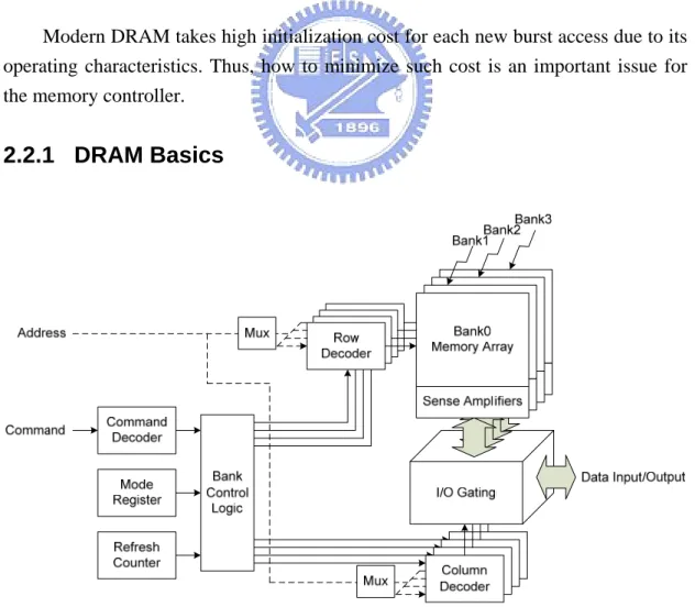
(18) ●. Protection unit support To enable both privileged and secure accesses, AXI provides three levels of protection unit support.. ●. Atomic operations AXI defines mechanisms for both exclusive and locked accesses.. ●. Error support AXI provides error support for both address decode errors and slave-generated errors.. ●. Unaligned address AXI supports unaligned burst start addresses to enhance the performance of the initial accesses within a burst.. 2.2 Modern DRAM Modern DRAM takes high initialization cost for each new burst access due to its operating characteristics. Thus, how to minimize such cost is an important issue for the memory controller.. 2.2.1 DRAM Basics. Fig. 2-4 Simplified DRAM architecture 10.
(19) Fig. 2-4 is a simplified DRAM architecture. In general, there are four bank of memory arrays with corresponding row and column decoders in one memory chip. Each bank of memory array consists of rows and each row consists of columns. The data width of one column equals to that of DRAM data bus. DRAM density size is the multiplication of the bank number in one chip, the row number in one bank, the column number in one row, and the data width of one column. When there is a read or write access, the accessed row must be loaded to sense amplifiers of the corresponding bank first. Then, columns are read from or written to the sense amplifiers. If the next access is to the same bank and row, columns can be accessed directly without reloading the row. However, if the next access is to different row in the same bank, DRAM has to write current row back to memory array from sense amplifiers and load needed one. Mode register stores DRAM settings including burst length, burst type, CAS latency, and etc. It should be configured during power-up initialization. The memory array stores data in small capacitors which lose charge over time. In order to retain data integrity, DRAM needs to recharge these capacitors. This process is done by loading data to sense amplifiers and writing back row by row. The refresh counter is used to generate row addresses necessary.. 2.2.2 DRAM Operations Now, we start to introduce DRAM operations in terms used in JEDEC standard [14][15]. Since there are slight differences between each DRAM type, we take DDR SDRAM as a representative. A.. Activation When the state of a bank is idle, a row must be “opened” before any READ or WRITE command can be issued to that bank. Opening one row is to load the row from memory array to sense amplifiers. This operation is accomplished by ACTIVE command. After the ACTIVE command, tRCD is required before a READ or WRITE command to that row to be issued. A subsequent ACTIVE command to a different row in the same bank can not be issued until the active row has been “closed” which 11.
(20) takes at least tRC. However, a subsequent ACTIVE command to another bank just needs a tRRD latency. B.. Read The read burst is initiated by a READ command with the bank and starting column address. During a read burst, the first valid data-out element from the starting column address will be available following CAS latency after the READ command is issued. C.. Write The write burst is initiated with a WRITE command and the bank and starting column address. During a write burst, the first valid data-in element will be registered following tDQSS after the WRITE command. After the last valid data-in element is registered, tWTR is required before a READ command to any bank and tWR before a PRECHARGE command to the same bank. D.. Precharge This operation writes the active row in sense amplifiers back to memory array. The bank will be available for a subsequent row activation tRP after the PRECHARGE command is issued. E.. Refresh Refresh operation retains data integrity in memory array. AUTO REFRESH command is used to initiate this operation every tREFC interval and tRFC should be met between two successive AUTO REFRESH commands. Note that, AUTO REFRESH command can only be issued when all banks are idle. F.. Power-down In DDR SDRAM standard, there are three power-down modes. These modes are precharge power-down, active power-down, and self refresh. Precharge power-down is entered when CKE is registered LOW and all banks are idle. Active power-down is entered when CKE is registered LOW and there is a row active in any bank. Self refresh is entered when CKE is registered LOW with all banks idle and AUTO REFRESH command.. 12.
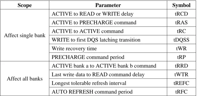
(21) Precharge power-down and active power-down do not refresh memory array automatically, so the power-down duration is limited by tREFC. However, self refresh does not have such limitation. Since precharge power-down and active power-down disable less functional units, they save less power while cost only several cycles to return original state. Self refresh disables almost all functional units, so it saves more power at the expense of several hundred return cycles.. Active. Bank0. Idle. Read / Write. Active. Precharge. ● ● ●. Refresh / Power-down. Active. Bank3. Idle. Active. Precharge. Fig. 2-5 Simplified DRAM state diagram. 13. Read / Write.
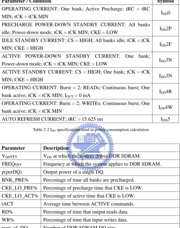
(22) Scope. Affect single bank. Affect all banks. Parameter. Symbol. ACTIVE to READ or WRITE delay. tRCD. ACTIVE to PRECHARGE command. tRAS. ACTIVE to ACTIVE command WRITE to first DQS latching transition. tRC tDQSS. Write recovery time. tWR. PRECHARGE command period. tRP. ACTIVE bank a to ACTIVE bank b command. tRRD. Last write data to READ command delay. tWTR. Longest tolerable refresh interval. tREFC. AUTO REFRESH command period. tRFC. Table 2-1 Key DDR SDRAM timings. Fig. 2-5 shows a simplified DRAM state diagram to provide a clear relationship between each operation. Table 2-1 lists key DDR SDRAM timings.. 2.2.3 DRAM Power Calculation Jeff Janzen proposed Calculating Memory System Power for DDR SDRAM in Micron designline, quarter 2, 2001 [16]. This article analyzes how DDR SDRAM consumes power and develops a method to calculate memory system power. This method can help memory sub-system power consumption estimation in high-level system evaluation before low-level hardware implementation. According to DDR SDRAM operations, memory system power consists of precharge power-down power, precharge standby power, active power-down power, active standby power, activate power, write power, read power, I/O power, and refresh power. Table 2-2 is the IDD specifications which can be looked up in data sheet. Table 2-3 is the parameters defined for equations in this article. All these parameters are used in power consumption calculation.. 14.
(23) Parameter / Condition. Symbol. OPERATING CURRENT: One bank; Active Precharge; tRC = tRC MIN; tCK = tCK MIN. IDD0. PRECHARGE POWER-DOWN STANDBY CURRENT: All banks idle; Power-down mode; tCK = tCK MIN; CKE = LOW. IDD2P. IDLE STANDBY CURRENT: CS = HIGH; All banks idle; tCK = tCK MIN; CKE = HIGH. IDD2F. ACTIVE POWER-DOWN STANDBY CURRENT: One bank; Power-down mode; tCK = tCK MIN; CKE = LOW. IDD3N. ACTIVE STANDBY CURRENT: CS = HIGH; One bank; tCK = tCK MIN; CKE = HIGH. IDD3N. OPERATING CURRENT: Burst = 2; READs; Continuous burst; One bank active; tCK = tCK MIN; IOUT = 0 mA. IDD4R. OPERATING CURRENT: Burst = 2; WRITEs; Continuous burst; One bank active; tCK = tCK MIN. IDD4W. AUTO REFRESH CURRENT; tRC = 15.625 ms. IDD5. Table 2-2 IDD specifications used in power consumption calculation. Parameter. Description. VDDsys. VDD at which the system drives DDR SDRAM.. FREQsys. Frequency at which the system applies to DDR SDRAM.. p(perDQ). Output power of a single DQ.. BNK_PRE%. Percentage of time all banks are precharged.. CKE_LO_PRE%. Percentage of precharge time that CKE is LOW.. CKE_LO_ACT% Percentage of active time that CKE is LOW. tACT. Average time between ACTIVE commands.. RD%. Percentage of time that output reads data.. WR%. Percentage of time that input writes data.. num_of_DQ. Number of DDR SDRAM DQ pins. num_of_DQS. Number of DDR SDRAM DQS pins Table 2-3 Parameters defined for equations. Fig. 2-6 shows the current usage on a DDR SDRAM device as CKE transitions. The current profile illustrates how to calculate precharge power-down and precharge standby power. Similarly, active power-down and active standby power can be calculated. 15.
(24) Fig. 2-6 Precharge power-down and standby current [16]. Precharge power-down power p(PRE_PDN) = IDD2P * VDD * BNK_PRE% * CKE_LO_PRE% Precharge standby power p(PRE_STBY) = IDD2F * VDD * BNK_PRE% * (1 – CKE_LO_PRE%) Active power-down power p(ACT_PDN) = IDD3P * VDD * (1 – BNK_PRE%) * CKE_LO_ACT% Active standby power p(ACT_STBY) = IDD3N * VDD * (1 – BNK_PRE%) * (1 – CKE_LO_ACT%). Fig. 2-7 Activate current [16]. 16.
(25) In Fig. 2-7, it is obvious that each pair of ACTIVE and PRECHARGE command consumes the same energy. Thus, activate power can be calculated by dividing total energy of all ACTIVE-PRECHARGE pairs by time. Activate power p(ACT) = (IDD0 – IDD3N) * tRC(spec) * VDD / tACT. Fig. 2-8 Write current [16]. Fig. 2-8 shows that IDD4W is required for write data input. Write power p(WR) = (IDD4W – IDD3N) * VDD * WR%. 17.
(26) Fig. 2-9 Read current with I/O power [16]. In Fig. 2-9, since the DRAM device drives external logics for read data output during a read access, extra I/O power is needed. Read power p(RD) = (IDD4R – IDD3N) * VDD * RD% I/O power p(DQ) = p(perDQ) * (num_of_DQ + num_of_DQS) * RD% The last power component is refresh power and its equation is shown below. Refresh power p(REF) = (IDD5 – IDD2P) * VDD So far, all equations use IDD measured in the operating condition listed in data sheet. However, the actual system may apply VDD and operating frequency other than those used in data sheet. Thus, the former equations have to be scaled by voltage supply and operating frequency. P(PRE_PDN) = p(PRE_PDN) * (use VDD)2 / (spec VDD)2 P(ACT_PDN) = p(ACT_PDN) * (use VDD)2 / (spec VDD)2 18.
(27) P(PRE_STBY) = p(PRE_STBY) * (use freq)2 / (spec freq)2 * (use VDD)2 / (spec VDD)2 P(ACT_STBY) = p(ACT_STBY) * (use freq)2 / (spec freq)2 * (use VDD)2 / (spec VDD)2 P(ACT) = p(ACT) * (use VDD)2 / (spec VDD)2 P(WR) = p(WR) * (use freq)2 / (spec freq)2 * (use VDD)2 / (spec VDD)2 P(RD) = p(RD) * (use freq)2 / (spec freq)2 * (use VDD)2 / (spec VDD)2 P(DQ) = p(DQ) * (use freq)2 / (spec freq)2 P(REF) = p(REF) * (use VDD)2 / (spec VDD)2 Then, sum up each scaled power component to get total power consumption. P(TOTAL). =. P(PRE_PDN) + P(PRE_STBY) + P(ACT_PDN) + P(ACT_STBY) + P(ACT) + P(WR) + P(RD) + P(DQ) + P(REF). 19.
(28) Chapter 3 Multimedia Platform Modeling In this chapter, the development of multimedia platform simulator is introduced. Section 3.1 is a brief introduction of why we need a simulator. Section 3.2 presents a generic multimedia platform for modeling. In Section 3.3, 3.4, and 3.5, each portion of the simulator is described.. 3.1 Introduction When starting to build our simulation environment, a key problem is how to balance coding time, flexibility, simulation speed, and accuracy of the simulator. HDL does not seem to be a good choice. First, it is developed in hardware view and that is, more regularity and less flexibility. Coding in hardware level has to follow a lot of constraints, so more coding time is required and the parameterization is bounded. Second, hardware implementation considers all signals. However, we only take care about some of them. Thus, eliminating useless parts to further speed up the simulator is more favorable. Is there a simple solution to provide short coding time, good flexibility, fast simulation speed, and most important, fine accuracy? As a result, SystemC [17] is chosen to construct our simulation environment. SystemC provides hardware-oriented constructs within the context of C++ as a class library implemented in standard C++. Also, SystemC provides an interoperable modeling platform which enables the development and exchange of very fast system-level C++ models. Thus, we can use C++ to implement signal-simplified simulator while keeping cycle accuracy.. 3.2 Multimedia Platform A generic multimedia SoC platform is shown in Fig. 3-1. There are 8 masters and 1 slave connected by the AXI bus interconnect. The 8 masters are CPU, DSP, accelerator, network, video in, video out, audio in, audio out and the only one slave is 20.
(29) the memory controller. CPU, DSP, and accelerator are the main data processing units. Network, video in, video out, audio in, and audio out are bridges to peripherals which communicate internal and external data exchange. The memory controller serves 8 masters to access data in the off-chip DRAM.. Fig. 3-1 Generic multimedia SoC platform. Fig. 3-2 shows the multimedia platform simulator block diagram. The scenario driver initiates one session of accesses of a master by enabling the corresponding master enable signal. One session of accesses means that the master generates transactions for data accesses according to its access pattern by one iteration. 8 different access patterns are used to model behaviors of each master in the generic multimedia SoC platform shown in Fig. 3-1.. 21.
(30) Fig. 3-2 Multimedia platform simulator block diagram. All data accesses conform to AXI protocol. However, to ease the development of simulator, we simplify the two AXI address channels, read and write, into one. This simplification does not affect AXI protocol compliance. The AXI network is responsible for channel arbitration with two common arbitration schemes, fixed priority and round-robin. The memory controller connects a simplified memory model. The memory model removes unnecessary operations such as refresh and power-down, and simplifies the input/output interface to facilitate using.. 3.3 Master Modeling Modeling a master can be thought as generating transactions after its behavior. According to AXI protocol, one transaction must possess at least four features which are ID, access type, destination address, and data to write. Here, the methods we use to generate transactions in our multimedia platform simulator are introduced.. 22.
(31) 3.3.1 ID Generation. Fig. 3-3 ID tag format. Since the multimedia platform is a multi-master platform, master information should be appended to ID tags to ensure their uniqueness. We use 8-bit ID tags in the simulator and the format is shown in Fig. 3-3. The most significant 3 bits are master ID and the rest 5 bits are transaction ID. Although transactions of the same master are done in order in our simulator and thus the transaction ID is useless, we still provide each transaction a transaction ID for simulator functionality correctness check.. 3.3.2 Type and Address Generation According to DRAM operating characteristics, it is obvious that transaction type and address affect DRAM access performance most. Thus, the transaction type and address generation is most important in master modeling. To generate transactions, an intuitive way is building behavioral model for each master. Although this method is most precise, implementation of each master is time-consuming. For efficiency and flexibility, we use a configurable transaction generator instead. The configurable transaction generator supports three access types and three address types. The three access types are read, write, and no operation. The three address types are 1-D, 2-D, and constraint random. Fig. 3-4 shows how addresses are generated by the three address types. Fig. 3-4(a) is the 1-D address type which increases the address from base address by a fixed offset. The offset is determined by the size of data transferred in one access. Most masters in the multimedia platform shown in Fig. 3-1 use 1-D address type. 23.
(32) Fig. 3-4(b) is the 2-D address type. Unlike the 1-D address type, there are one start address and one end address in a row. Thus, the address cannot be increased directly until the end of row. When the end address of a row is met, the address jumps to the start address of the next row and goes on increasing. The boundary between the start and end address is usually fixed and preset. The 2-D address type is used in modern block-based video encoding and decoding, such as MPEG-2, MPEG-4, and H.264. Fig. 3-4(c) is the constraint random address type which generates address randomly in the master mapping space. CPU accesses are always in such kind of address type.. (a). (b). 24.
(33) (c) Fig. 3-4 (a) 1-D address type (b) 2-D address type (c) Constraint random address type. Fig. 3-5 A simple transaction generation example. Fig. 3-5 gives a simple example to illustrate how the configurable transaction generator works. The transaction generator is configured by a file in the format shown in bottom of Fig. 3-5. The first column is the transaction type which includes read,. 25.
(34) write, and no operation. The second is the number of data to be accessed. The third and forth are address type and base address respectively. In this example, the transaction generator has three states (The number of states equals the number of rows in the configuration file). The first state generates 32 data writes in 1-D address type from base address 0x2000 and the number of write transactions depends on the preset burst length. Once a write transaction is generated, until it is sent out via the AXI network, the next one cannot be generated. Thus, it may take over 32 cycles in this state. Since this state is a write state, all transactions are followed by their write data. The write data generation will be stated later. The second state is a NOP state and it doesn’t generate any transaction. Thus, the configurable transaction generator idles for 8 cycles. The last state is a read state and it works like the write state described before except that it doesn’t have to generate write data.. 3.3.3 Write Data Generation Every time a write transaction is generated, the corresponding write data is also brought out. Although the content of write data has nothing with DRAM access performance, we still define a write data format which is shown in Fig. 3-6 to ease the simulator functionality correctness check. As presented in Fig. 3-6, the first column is the ID tag of the write transaction. The second is a hexadecimal string “data”. The last one is the order of the write data in a burst. For example, the write data of a write transaction with ID tag 0x10 and burst length 2 are “0x10data0” and “0x10data1”.. Fig. 3-6 Write data format. 26.
(35) 3.4 AXI Network Since the AXI channels are uncorrelated, the AXI network arbitration can be implemented to each channel independently. As to the arbitration schemes, fixed priority and round-robin are used in our simulator. It is shown in Fig. 3-7 that master 0 always takes highest priority and master 7 always takes lowest when the fixed priority scheme is applied. Fig. 3-8 shows the round-robin scheme. It is composed of eight states and the state changes each time when the arbitration is done. In the first state, master 0 takes the highest priority and master 7 takes the lowest. In the second state, master 1 takes the highest priority and master 0 takes the lowest and so on. Thus, in the last state, master 7 takes the highest priority and master 6 takes the lowest.. Fig. 3-7 Fixed priority arbitration scheme. 27.
(36) Fig. 3-8 Round-robin arbitration scheme. 28.
(37) 3.5 Memory Controller There are two type of memory controllers implemented. The difference is whether it supports bank-interleaving or not.. 3.5.1 Memory Controller without Bank-interleaving Support. Fig. 3-9 Block diagram of the memory controller without bank-interleaving support. Fig. 3-9 is the block diagram of the memory controller without bank-interleaving support. It uses six processes and each process will be described below. Every time the bus_get_req receives a transaction ID, type, and address, it stores them in the bus_get_req buffer. Also, when the bus_get_wdata receives one set of transaction ID and write data, it stores them in the bus_get_wdata buffer. The trans_schedule determines the order of transactions in the bus_get_req buffer executed by the bank_ctrl. We implement three different transaction scheduling policies which will be stated in Section 3.5.3.. 29.
(38) After the trans_schedule reorders the input transactions, the bank_ctrl translates these transactions into DRAM commands. The translation depends not only on the transaction type and address, but also on the current bank state. Fig. 3-10 shows all three possible cases in the transaction to command translation.. (a). (b). (c) Fig. 3-10 Bank state transition and related commands when (a) current bank state is idle (b) current bank state is active with row hit (c) current bank state is active with row miss. 30.
(39) In Fig. 3-10(a), the current bank state is idle and an ACTIVE command is issued to open a row for the transaction access. In Fig. 3-10(b), the current bank state is active and the transaction accesses the opened row, that is, row hit. Thus, a READ or WRITE command can be issued directly without opening a row. In Fig. 3-10(c), the current bank state is active and the transaction accesses a row other than the opened row, that is, row miss. Before a READ or WRITE command can be issued, the PRECHARGE and ACTIVE command must be applied to close the current row and open the wanted row. It is obvious that the row hit case needs fewest commands to finish a transaction while the row miss case requires most commands. To finish a transaction using fewer commands represents better DRAM access performance and less DRAM power consumption. The transaction scheduling by the trans_schedule is to increase row hit cases and reduce row miss cases. When a command is generated, the bank_ctrl puts necessary information on the command and address bus. Then it triggers the memory model by the bank_ena signal. If the transaction is a write transaction, bank_ctrl gets the corresponding write data via ID matching from the bus_get_wdata buffer and puts it on the data bus after the memory model is triggered with a WRITE command. When the write transaction is finished, bank_ctrl triggers the bus_send_resp process by the send_resp_ena signal to send the master a response. If the transaction is a read transaction, bank_ctrl gets read data from data bus after the memory model is triggered with a READ command. Then, it utilizes the bus_send_rdata process to send read data to the AXI network. For simplicity, we assume that masters are always ready to receive the response after issuing a write transaction and read data after issuing a read transaction. Thus, no output buffer is needed.. 31.
(40) 3.5.2 Memory Controller with Bank-interleaving Support Within the constraint of common input and output buses, the four DRAM banks can operate in parallel which is called bank-interleaving. When bank-interleaving is utilized, we can overlap the waiting latencies of DRAM operations in different banks to achieve lower effective latencies.. A Channel. bus_get_req trans_schedule0. WD Channel. bus_get_wdata. bank_ctrl3 bank_ctrl2 bank_ctrl1 bank_ctrl0. Memory Model bank_ena. bank0. address cmd_schedule command data. bank1 bank2 bank3. RD Channel. WR Channel. send_data_ena bus_send_rdata. bus_send_resp. rdata. send_resp_ena. Fig. 3-11 Block diagram of the memory controller with bank-interleaving support. Fig. 3-11 is the block diagram of the memory controller with bank-interleaving support. There are four isolated trans_schedule and bank_ctrl pairs to generate commands for each bank. The bank_ctrl can only handle commands for one bank. To process the overall command issue, cmd_schedule is used. To determine which bank can issue the command, we first calculate the “score” of each bank. The score is computed by a function of command lasted time and command type. Then, the bank with highest score is selected for command issue. If there are two or more banks with equal score, bank 0 has the highest priority and bank 3 has the lowest. The commands which are not issued will be carried on by each bank_ctrl. We implement three different scoring functions for the cmd_schedule. Each of them is shown in Section 3.5.4. 32.
(41) 3.5.3 Transaction Scheduling Policy. (a). (b). 33.
(42) (c) Fig. 3-12 Examples of (a) first in first serve (FIFS) policy (b) two level round-robin (TLRR) policy (c) modified first in first serve (MFIFS) policy. A.. First in first serve (FIFS) Fig. 3-12(a) is an example. When the FIFS policy is applied, the output order of transactions is the same as the input order in spite of which master the transaction comes from.. B.. Two level round-robin (TLRR) When this policy is applied, we separate the masters into two levels, a high priority and a low priority level. Transactions from masters in high priority level are output first. As to the output order of transactions in the same level, round-robin scheme is utilized. Of course, transactions from the same master are output in input order. In our simulator, only master 0 (CPU in the multimedia platform) is set to high priority level. Therefore, in Fig. 3-12(b) the two transactions from master 0 are output first and then transactions from master 1 and master 2 rotate. We implement the TLRR policy which works pretty well in [9] for comparison... 34.
(43) C.. Modified first in first serve (MFIFS) Based on the assumption that transaction types from the same master are likely the same and transaction addresses from the same master are likely sequential, we propose this policy. According to the assumption, bundling transactions from the same master together provides the memory controller more chances to perform successive DRAM read or write operations. However, although successive processing of transactions from one master can increase overall DRAM performance, it also increases latencies of transactions from other masters. To balance the performance improvement and the latency increment, we set a threshold to limit the maximum number of transactions in each successive processing. We set the threshold to be 2 in the example shown in Fig. 3-12(c). First, as FIFS policy, the transaction from master 0 is output. Then, follow the input order to search another transaction from master 0 in the transaction buffer. If there is one, it is the next output. If there is none, the successive processing terminates. In Fig. 3-12(c), there is one and it is the last one in this successive processing since the threshold is 2. After that, continue to apply FIFS policy to find the starting transaction of next successive processing.. 3.5.4 Scoring Function A.. Lasted time only (LTO) Before calculating the score, the validity of commands from each bank controller is examined. If the command is a NOP command or it cannot be issued at this time due to timing constraints of DRAM, the score is set to zero. Since zero score is used for such case, the score must larger than one in other cases. Thus, the scoring function is as below. score = command_lasted_time + 1. 35.
(44) B.. Lasted time over type (LTOT) if(command_type == PRECHARGE) score = command_lasted_time*4 + 3 else if(command_type == ACTIVE) score = command_lasted_time*4 + 2 else if(command_type == READ) score = command_lasted_time*4 + 1 else if(command_type == WRITE) score = command_lasted_time*4 + 1. The scoring function above makes the weight of command lasted time over that of command type. Thus, commands with longer lasted time always get higher scores. As to commands with equal lasted time, the command type determines. Because each bank operates independently, if proper utilized, latencies between two successive access commands (READ to READ, READ to WRITE, WRITE to READ, and WRITE to WRITE) can be hidden. Since the row miss case has longest latency, the PRECHARGE command pluses 3 points. With median latency, the ACTIVE command pluses 2 points. The 1 point for READ and WRITE commands is used to prevent zero score. C.. Lasted time with type (LTWT) if(command_type == PRECHARGE) score = command_lasted_time*2 + 3 else if(command_type == ACTIVE) score = command_lasted_time*2 + 2 else if(command_type == READ) score = command_lasted_time*2 + 1 else if(command_type == WRITE) score = command_lasted_time*2 + 1. The scoring function is like that of LTOT. The only difference is that the factor of command lasted time is reduced to 2. Thus, the PRECHARGE and ACTIVE commands have more chances to be issued earlier.. 36.
(45) Chapter 4 Simulation Result and Analysis This chapter consists of three parts. Section 4.1 introduces several scenarios which can be applied to the simulator. Section 4.2 describes the settings of video phone scenario utilized in our simulation. In Section 4.3, simulation result and analysis are presented.. 4.1 Introduction Scenario. Description. Master / Task. Movie Playback. Play a movie from CPU / OS the storage DSP & Accelerator / Audio & video decoding Audio Out / Output sound Video Out / Display video. DTV Service. Play DTV programs CPU / OS from digital broadcast DSP & Accelerator / Audio & video decoding Network / Radio broadcast bitstream Audio Out / Output sound Video Out / Display video. Video Phone. Video phone. CPU / Audio codec & OS DSP / Video decoding Accelerator / Video encoding Network / Communication bitstream Audio In / Voice capture Audio Out / Output voice Video In / Video capture Video Out / Display video. Table 4-1 Examples of scenarios which can be applied to the multimedia platform simulator. Since the multimedia platform simulator is configurable by access pattern files, it can be easily modified to perform many different scenarios. According to the 37.
(46) simulation result, the DRAM performance and power consumption introduced by the memory controller are evaluated. After that, the evaluation result can be taken into consideration for hardware implementation. Table 4-1 lists examples of the scenario which can be applied to the multimedia platform simulator. We use the video phone scenario in our simulation because it utilizes all masters and is the most complicated case.. 4.2 Simulation Environment Setting The detailed settings of the video phone scenario are listed below. Table 4-2 shows the task allocation to each master and the access patterns generated according to the task allocation. Table 4-3 lists the bandwidth requirement and timing constraint of each master based on Table 4-2. The memory mapping is shown in Fig. 4-1. As to other important settings of the simulator, we use 32-bit AXI data bus is and 16-bit memory data bus. The timing and power parameters of the memory model is the same as Micron’s MT46V8M16 DDR SDRAM [18]. Both the memory controller and DRAM operate at 200 MHz clock rate. Master. Task. Access Pattern. CPU. Audio Codec OS. Read bitstream and PCM data Write bitstream and PCM data Random reads and writes for OS. DSP. Video decoding Miscellaneous routine. Read reference macroblock Write reconstructed macroblock (YUV) Write reconstructed macroblock (RGB) Random reads and writes. Accelerator. Video encoding. Read reference macroblock Write reconstructed macroblock (YUV) Write reconstructed macroblock (RGB) Random reads and writes. Network. Tx/Rx bitstream. Read bitstream Write bitstream. Audio In. Audio input. Write PCM data. Audio Out. Audio output. Read PCM data. Video In. Video input. Write capture video (RGB). Video Out. Video output. Read display video (RGB) 38.
(47) Table 4-2 Tasks and the corresponding access patterns of the video phone scenario. Master. Bandwidth Requirement. Timing Constraint. CPU. 16.14 MB/sec. 24 ms. DSP. 72.48 MB/sec. 33 ms. Accelerator. 70.94 MB/sec. 33 ms. Network. 2.30 MB/sec. 33 ms. Audio In. 8.46 MB/sec. 24 ms. Audio Out. 8.46 MB/sec. 24 ms. Video In. 36.86 MB/sec. 33 ms. Video Out. 36.86 MB/sec. 33 ms. Total. 252.5 MB/sec. N/A. Table 4-3 Bandwidth requirement and timing constraint of the video phone scenario. 0x3F_FFFF. 0x7F_FFFF. 0xBF_FFFF. DSP 3MB. 0xFF_FFFF. CPU 3MB. Reserved Reserved. 0x90_0000. 4 MB. 0xD0_0000. Reserved 0x47_0600. 0x87_0600. Audio In PCM 4KB. 0x06_F600. Audio Out PCM 4KB. 0x46_F600. Bitstream Out 297 KB 0x02_5200. 0x00_0000. Video In RGB 297 KB. Video Out RGB 297 KB 0x82_5200. Decoding Frame 1 YUV 148.5 KB 0x40_0000. Bank 0. 0xC6_F600. 0x86_F600. 0x42_5200. Decoding Frame 0 YUV 148.5 KB. Reserved. Encoding Frame 0 YUV 148.5 KB 0x80_0000. Bank 1. Bank 2. Fig. 4-1 Memory mapping of the video phone scenario. 39. Bitstream In 297 KB 0xC2_5200. Encoding Frame 1 YUV 148.5 KB 0xC0_0000. Bank 3.
(48) 4.3 Simulation Result and Analysis 4.3.1 DRAM Bandwidth Utilization First Instead of trying all possible combinations of each parameter, we use a simpler method to develop the memory controller. First, we determine the data burst length since it affects the simulation result most. Based on chosen burst length, scoring functions for the command scheduler are evaluated. After that, we use the selected burst length and scoring function to find out a proper transaction scheduling policy. During the memory controller development process, both two AXI network arbitration schemes are applied to see the bus arbitration scheme effect. A.. Simulation 1 – Choose a proper data burst length Buffer size. 8 entries. Data burst length. 2, 4, 8. Bank-interleaving support. Yes / No. Scoring function. LTO. Transaction scheduling policy. FIFS. Table 4-4 Configuration of the simulator in simulation 1. In simulation 1, different data burst lengths are applied to the memory controller with/without bank-interleaving support. Table 4-4 lists the configuration of the simulator. Data burst length. 2. 4. Without bank-interleaving. Violated Violated. With bank-interleaving. Violated. Met. 8 Violated Met. Table 4-5 Timing constraint status when fixed priority bus arbitration scheme is applied. 40.
(49) Average DRAM Bandwidth Utilization - Fixed Priority 100.00% 90.00% 80.00%. Bandwidth utilization. 70.00% 60.00% Without interleaving With interleaving. 50.00% 40.00% 30.00% 20.00% 10.00% 0.00% Burst length 2. Burst length 4. Burst length 8. Fig. 4-2 Average DRAM bandwidth utilization with fixed priority bus arbitration scheme. Table 4-5 tells whether the timing constraints are met with each configuration when the fixed priority bus arbitration scheme is applied. Except for burst length 2, the timing constraints are met with bank-interleaving support. Fig. 4-2 shows the average DRAM bandwidth utilization with fixed priority bus arbitration scheme. Without bank-interleaving support, burst length 2 gets lowest bandwidth utilization 26.5% while burst length 8 gets highest 41.6%. With bank-interleaving support, burst length 2 still gets lowest bandwidth utilization 27.1% while burst length 8 remains highest 59.3%. With bank-interleaving support, the average bandwidth utilization improvement from burst length 2 to 8 is 2.1%, 55.9%, and 42.8% respectively. Data burst length. 2. 4. 8. Without bank-interleaving. Violated Violated. Met. With bank-interleaving. Violated. Met. Met. Table 4-6 Timing constraint status when round-robin bus arbitration scheme is applied. 41.
(50) Average DRAM Bandwidth Utilization - Round-robin 100.00% 90.00% 80.00%. Bandwidth utilization. 70.00% 60.00% Without interleaving With interleaving. 50.00% 40.00% 30.00% 20.00% 10.00% 0.00% Burst length 2. Burst length 4. Burst length 8. Fig. 4-3 Average DRAM bandwidth utilization with round-robin bus arbitration scheme. Table 4-6 tells whether the timing constraints are met with each configuration when the round-robin bus arbitration scheme is applied. Except for burst length 2, the timing constraints are met with bank-interleaving support. Fig. 4-3 shows the average DRAM bandwidth utilization with round-robin bus arbitration scheme. Without bank-interleaving support, burst length 2 gets lowest bandwidth utilization 16.5% while burst length 8 gets highest 46.8%. With bank-interleaving support, burst length 2 still gets lowest bandwidth utilization 20.0% while burst length 8 remains highest 67.0%. With bank-interleaving support, the average bandwidth utilization improvement from burst length 2 to 8 is 21.5% , 60.3%, and 43.1% respectively. Note that when the burst length is 2, the average bandwidth utilization with round-robin is 25% to 35% lower than that with fixed priority. When the burst length is 4, the average bandwidth utilizations with both bus arbitration schemes are almost the same. And when the burst length is 8, the average bandwidth utilization with round-robin is 10% to 15% higher than that with fixed priority. Since transactions from the same master are not closely bundled together in time, there exists small intervals between two successive transactions. Therefore, the fixed priority bus arbitration scheme often causes transactions from two masters rotates. If the two masters are mapped to the same bank, row miss occurs repeatedly. If the two masters 42.
(51) generate transactions with different transaction types in a period, read-write turnaround happens over and over in that period. The two reasons make bandwidth utilization improvement diminished. It is obvious that whether which bus arbitration scheme is applied or whether there is bank-interleaving support, burst length 8 always gets highest bandwidth utilization. Hence, we set the data burst length to 8 in the following simulations. B.. Simulation 2 – Choose a proper scoring function Buffer size. 8 entries. Data burst length. 8. Bank-interleaving support. Yes. Scoring function. LTO, LTOT, LTWT. Transaction scheduling policy. FIFS. Table 4-7 Configuration of the simulator in simulation 2. Different scoring functions are applied in simulation 2 and Table 4-7 lists the configuration of the simulator.. Average DRAM Bandwidth Utilization 100.00% 90.00% 80.00%. Bandwidth utilization. 70.00% 60.00% LTO LTOT LTWT. 50.00% 40.00% 30.00% 20.00% 10.00% 0.00% Fixed priority. Round-robin. Fig. 4-4 Average DRAM bandwidth utilization with different scoring functions. 43.
(52) Fig. 4-4 shows the average DRAM bandwidth utilization with different scoring functions. Both LTOT and LTWT work well when fixed priority is applied, the improvement is 17.7% and 17.4% individually. However, LTOT and LTWT works bad when round-robin is applied, the deterioration is 0.4% and 0.8% respectively. Since the fixed priority bus arbitration scheme provides less parallelism for bank-interleaving, row miss latency hiding by LTOT or LTWT improves the bandwidth utilization a lot. On the contrary, round-robin provides sufficient parallelism for bank-interleaving. Thus, LTOT and LTWT may not benefit. Because LTOT performs slightly better, we set the scoring function to LTOT. C.. Simulation 3 – Choose a proper transaction scheduling policy Buffer size. 8 entries. Data burst length. 8. Bank-interleaving support. Yes. Scoring function. LTOT. Transaction scheduling policy. FIFS, TLRR, MFIFS. Table 4-8 Configuration of the simulator in simulation 3. Different transaction scheduling policies are evaluated in simulation 3 and Table 4-8 lists the configuration of the simulator. Fig. 4-5 shows the average DRAM bandwidth utilization with different transaction scheduling policies. When the bus arbitration scheme is fixed priority, TLRR is 8.7% worse and MFIFS is 2.8% better than FIFS. When the bus arbitration scheme is round-robin, TLRR is 7.8% worse and MFIFS is 6.1% better than FIFS. Since TLRR is designed for the multimedia platform with dedicated channels to masters, it cannot work well with limited information caused by single on-chip bus and finite buffer size. Of course, we choose MFIFS as the final transaction scheduling policy. However, the performance of MFIFS may differ with different buffer sizes and thresholds. Thus, an extra simulation is performed.. 44.
(53) Average DRAM Bandwidth Utilization 100.00% 90.00% 80.00%. Bandwidth utilization. 70.00% 60.00% FIFS TLRR MFIFS. 50.00% 40.00% 30.00% 20.00% 10.00% 0.00% Fixed priority. Round-robin. Fig. 4-5 Average DRAM bandwidth utilization with different transaction scheduling policies. D.. Simulation 4 – Choose a proper buffer size and threshold for MFIFS Buffer size. 4, 8, 12, 16 entries. Data burst length. 8. Bank-interleaving support. Yes. Scoring function. LTOT. Transaction scheduling policy. MFIFS. MFIFS threshold. 2, 3, 4. Table 4-9 Configuration of the simulator in simulation 4. In simulation 4, different buffer sizes and thresholds are tested. Table 4-9 lists the configuration of the simulator.. 45.
(54) Average DRAM Bandwidth Utilization 100.00% 90.00% 80.00%. Bandwidth utilization. 70.00% FP_TH2 FP_TH3 FP_TH4 RR_TH2 RR_TH3 RR_TH4. 60.00% 50.00% 40.00% 30.00% 20.00% 10.00% 0.00% Buffer size 4. Buffer size 8. Buffer size 12. Buffer size 16. Fig. 4-6 Average DRAM bandwidth utilization with different buffer sizes and thresholds. Fig. 4-6 shows the average DRAM bandwidth utilization with different buffer sizes and thresholds. When the buffer size is 4, it bounds the bandwidth utilization since the memory controller cannot get sufficient information. When the buffer size is 12, the two bus arbitration schemes can merely affect the bandwidth utilization. Fig. 4-7 and Fig. 4-8 presents the average transaction latency and DRAM power consumption individually. In Fig. 4-7, larger buffer size with equal transaction processing ability leads to longer latency. However, larger threshold does not inevitably increase the average transaction latency since it may slightly increase the latency of other masters while significantly decrease the latency of one master. Based on Fig. 4-6, take Fig. 4-7 and Fig. 4-8 as reference, buffer size 12 and threshold 4 are chosen.. 46.
(55) Average Transaction Latency 300. 250. Latency (ns). 200 FP_TH2 FP_TH3 FP_TH4 RR_TH2 RR_TH3 RR_TH4. 150. 100. 50. 0 Buffer size 4. Buffer size 8. Buffer size 12. Buffer size 16. Fig. 4-7 Average transaction latency with different buffer sizes and thresholds. Average DRAM Power Consumption 600. 500. Power (mW). 400 FP_TH2 FP_TH3 FP_TH4 RR_TH2 RR_TH3 RR_TH4. 300. 200. 100. 0 Buffer size 4. Buffer size 8. Buffer size 12. Buffer size 16. Fig. 4-8 Average DRAM power consumption with different buffer sizes and thresholds. 47.
(56) E.. Summary. Average DRAM Bandwidth Utilization Transition 100.00% 90.00% 80.00%. Bandwidth utilization. 70.00% 60.00% Fixed priority Round-robin. 50.00% 40.00% 30.00% 20.00% 10.00% 0.00% Without bankinterleaving. With bankinterleaving. With LTOT. With MFIFS. With buffer size and threshold modification. Fig. 4-9 Average DRAM bandwidth utilization transition through the simulations. Average Transaction Latency Transition 500 450 400 350. Time (ns). 300 Fixed priority Round-robin. 250 200 150 100 50 0 Without bankinterleaving. With bankinterleaving. With LTOT. With MFIFS. With buffer size and threshold modification. Fig. 4-10 Average transaction latency transition through the simulations. 48.
(57) Average DRAM Power Consumption Transition 600. 500. Power (mW). 400. Fixed priority Round-robin. 300. 200. 100. 0 Without bankinterleaving. With bankinterleaving. With LTOT. With MFIFS. With buffer size and threshold modification. Fig. 4-11 Average DRAM power consumption transition through the simulations. Fig. 4-9 , Fig. 4-10, and Fig. 4-11 shows the average DRAM bandwidth utilization, transaction latency, and power consumption transitions through simulations. In Fig. 4-10, when bank-interleaving is supported, the average transaction latency is reduced by 53.6% with fixed priority bus arbitration scheme and 33.9% with round-robin. The significant reduction is because bank-interleaving can efficiently hide DRAM operation latencies. According to Fig. 4-9 and Fig. 4-11, when the bus arbitration scheme is fixed priority, the bandwidth utilization is improved by 72.8% with 36.1% more power consumption. When the bus arbitration scheme is round-robin, the bandwidth utilization is improved by 53.3% with 11.9% more power consumption. Note that MFIFS with buffer size and threshold modification can slightly increase the bandwidth utilization while decrease the power consumption up to 13%.. 4.3.2 DRAM Power Consumption First Since the video phone scenario does not require up to 71.8% bandwidth utilization to finish all tasks, reduce bandwidth utilization to achieve lower power 49.
(58) consumption is more favorable in the embedded system. In order to reduce power, we analyze the DRAM power consumption. The DRAM power components listed in Section 2.2.3 can be divided into the background power, activate power, and read/write power. The background power consists of the precharge power-down power, precharge standby power, active power-down power, active standby power, and refresh power. In our simulation environment, DRAM is always in the active standby state. Thus, the effective background power is the summation of active standby power and refresh power. Therefore, the background power is fixed at all time. The activate power is determined by the number of total ACTIVE commands and the task execution time. Thus, fewer ACTIVE commands or longer task execution time can lower activate power. The read/write power is composed of the read power, write power, and I/O power. The read power and I/O power are decided by the number of total data reads and the task execution time. Also, the write power is decided by the number of total data writes and the task execution time. To lower read/write power, just reduce the read or write data count and stretch the task execution time. However, with the same access pattern, the number of data reads or writes is determined by the data burst length. Since the memory controller with shorter data burst length reads or writes fewer extra data, it consumes less power. According to above analysis, to reduce DRAM power consumption, we should reduce the number of ACTIVE commands and the data burst length, and stretch the task execution time within timing constraints. Take Table 4-5, Table 4-6, Fig. 4-9, and Fig. 4-11 into consideration, we choose the memory controller with data burst length 4, MFIFS transaction scheduling policy, and without bank-interleaving support. Though it may consume less power with data burst length 2, the probability of timing violation is also larger. Take Fig. 4-7 as the reference, we set all buffer size to 4 and the MFIFS threshold to 2 to suppress the increase of bandwidth utilization which stretches the task execution time.. 50.
(59) Fixed priority. Round-robin. 42.9%. 36.8%. 356.9 mW. 423.4 mW. Average DRAM bandwidth utilization Average DRAM power consumption. Table 4-10 Average DRAM bandwidth utilization and power consumption with different bus arbitration schemes. Table 4-10 lists the simulation result and there is no timing violation. Compared with the result in Section 4.3.1, the average DRAM power consumption is reduced by 26.3% with fixed priority bus arbitration scheme and 13.2% with round-robin.. Average DRAM Power Consumption 600. 500. Power (mW). 400 Total read/write power Total activate power Total background power. 300. 200. 100. 0 Fixed priority & bandwidth first. Fixed priority & power first. Round-robin & bandwidth first. Round-robin & power first. Fig. 4-12 Average DRAM power consumption with different optimization policies. Fig. 4-12 shows each power component of the average DRAM power consumption with bandwidth utilization first and power consumption first. The background power is always fixed and takes about 30% of total power consumption. When the fixed priority bus arbitration scheme is applied with power first, the activate and read/write power is reduced by 24.4% and 40.0% respectively. When the round-robin bus arbitration scheme is applied with power first, although the activate power increases by 116.2%, the reduction of read/write power by 48.5% still lowers total power consumption.. 51.
(60) The result is not optimized. However, it is hard to find out an optimized result without thorough simulations since the related factors are not independent and affect each other.. 52.
(61) Chapter 5 Hardware Implementation There are two sections in the chapter. Section 5.1 describes the hardware design of memory controller. In Section 5.2, the implementation result is shown.. 5.1 Hardware Design. Fig. 5-1 Hardware block diagram of the memory controller. In Section 4.3.1, we have developed a high performance memory controller architecture. Also, in Section 4.3.2, a low power with less performance architecture by reducing the applied techniques is presented. In real applications, the later one should be implemented since it completes all tasks with less cost. However, because we are eager to know the hardware cost when all techniques are applied, the former one is implemented.. 53.
數據
+7
![Fig. 2-6 Precharge power-down and standby current [16]](https://thumb-ap.123doks.com/thumbv2/9libinfo/8743577.204538/24.892.197.698.114.338/fig-precharge-power-down-and-standby-current.webp)
![Fig. 2-8 Write current [16]](https://thumb-ap.123doks.com/thumbv2/9libinfo/8743577.204538/25.892.195.694.297.717/fig-write-current.webp)
相關文件
American Association of School Librarians, Association for Educational Communications and Technology.. Information power: Building partnerships
200kW PAFC power plant built by UTC Fuel Cells.. The Solar
• Early experiences have long term impacts on brain power.. • Creative play and quality care make all
真實世界的power delay
87 Eivind Almaas and Albert-László Barabási (2006), “Power laws in biological networks”, in Power Laws, Scale-Free Networks and Genome Biology, Ed. Karev (Eurekah.com and
Lecture 16: Three Learning Principles Occam’s Razor?. Sampling Bias Data Snooping Power
• Power Level: in favors of the more powerful party, regardless of right or fairness. • Right Level: based on relevant standards
“Reliability-Constrained Area Optimization of VLSI Power/Ground Network Via Sequence of Linear Programming “, Design Automation Conference, pp.156 161, 1999. Shi, “Fast
