國 立 交 通 大 學
電機學院 IC 設計產業研發碩士班
碩 士 論 文
以電子系統層級實作 WiMAX 系統中
錯誤偵測與錯誤校正的行為模型
An Error Detection & Correction Behavior Model Implementation
for WiMAX System at Electronic System Level
研 究 生:呂亦琦
指導教授:黃經堯
教授
以電子系統層級實作 WiMAX 系統中
錯誤偵測與錯誤校正的行為模型
An Error Detection & Correction Behavior Model Implementation for
WiMAX System at Electronic System Level
研 究 生:呂亦琦
Student
:Yi-Chi Lu
指導教授:黃經堯 博士
Advisor
:Dr. Ching-Yao Huang
國 立 交 通 大 學
電機學院 IC 設計產業研發碩士班
碩 士 論 文
A Thesis
Submitted to College of Electrical & Computer Engineering
National Chiao Tung University
in Partial Fulfillment of the Requirements
for the Degree of
Master
in
Industrial Technology R & D Master Program on
IC Design
Hsinchu, Taiwan, Republic of China
以電子系統層級實作 WiMAX 系統中
錯誤偵測與錯誤校正的行為模型
學生:呂亦琦
指導教授:黃經堯 博士
國立交通大學電機學院產業研發碩士班
摘
要
SoC Designer 是一個電子系統層級模擬平台,適合用來做為通訊系統的設計與驗 證。為了解決傳送端與接收端之間封包的傳送,我們建立的一個行為模型來模擬傳送 端,接收端,與傳輸通道的功能,並且保證資料傳送的完整性。本論文直接從系統規格 書開始,實現通訊系統中錯誤偵測與錯誤校正的行為模型,確定功能正確無誤,將行為 模型從個人電腦的平台移到 SoC Designer 的平台上執行,並且提出一個 Virtual Socket 的概念解決封包傳輸的問題。這個模擬平台也可以做軟體/硬體共同模擬,Hardware Modeling 的好處是可以節省模擬的時間。經過模擬,證明可以節省模擬時間,改善系統 驗證的效率。An Error Detection & Correction Behavior Model Implementation for
WiMAX System at Electronic System Level
Student:Yi-Chi Lu Advisor:Dr. Ching-Yao Huang
Industrial Technology R & D Master Program of
Electrical and Computer Engineering College
National Chiao-Tung University
ABSTRACT
SoC Designer is an electronic system level simulation platform and is suitable for the
communication system design and verification. In order to model the communication between
the transmitter and the receiver, we implement a behavior model which includes the
transmitter, the receiver and the channel. Besides we guarantee the data integrity in the
transmission. We establish our behavior model according to the IEEE802.16 specification.
After developing the prototype on the PC platform, we port the behavior model to the SoC
with the packet transmission. The platform also supports the hardware/software co-simulation
and the simulation time will be decreased by hardware modeling technology. According to the
誌
謝
很高興終於完成論文了。 除了感謝自己沒有放棄,首先要感謝的是黃經堯教授賦予了大家豐富的資源和環 境,給予精闢的教導並在研究上給予方向,在教授細心的指導下,完成了這篇碩士論文。 另外,感謝各位口試委員們-曹孝櫟教授與李永定博士,提供寶貴的建議與指教。 感謝實驗室的同學-俊宇、宗翰、子宗、育澤、冠穎,理銓,還有實驗室的學長和 學弟,在課業和日常生活上,大家總是相互的扶持幫助,以及在學業上的討論與切磋。 感謝我的女朋友-怡秀,從我們大學認識,畢業後當兵,到園區上班,最後再重新 回學校進修,謝謝妳一直陪伴在我身邊。 最後,我要感謝我的家人,他們無怨無悔的付出與鼓勵,使我求學過程中無後顧之 憂,僅以此論文與我的家人及好友分享我的收穫與喜悅,願他們永遠平安、順心。 誌予 2007 呂亦琦Contents
摘要 i
Abstract ii
致謝 iv
Contents v
List of Figures viii
List of Tables xi
Chapter 1 Introduction 1
1.1 Technology Trend... 1
1.2 Motivation ... 1
1.3 The Focus of Our Work ... 4
1.4 Brief in WiMAX... 4
1.5 Organization ... 6
Chapter 2 Related Work 7 2.1 SoC Design and Verification Issue ... 8
2.2.1 MAC Management Message ... 11
2.2.2 Header and Subheader ... 13
2.2.3 Automatic Repeat Request... 16
2.2.4 Cyclic Redundancy Check... 16
2.3 Design and Verification Language ... 17
2.3.1 Hardware Modeling... 19 2.3.2 SystemC... 20 2.4 Platform-based Design ... 21 2.4.1 AMBA ... 22 2.4.2 The HW/SW Interaction ... 24 2.4.3 Hardware Registers... 26 2.4.4 Memory Mapping ... 26
2.5 Virtual Socket Concept ... 28
2.5.1 Simulation Platform and Architecture ... 28
2.5.2 Downlink and Uplink Procedure ... 29
2.6 Summary ... 31
Chapter 3 Case Study:A Behavior Model Design 32 3.1 Our Design Flow for Behavior Model... 32
3.1.1 Reference Software Development ... 34
3.1.2 Simulation on ADS and ESL Platform ... 36
3.1.3 System Level Simulation with Pure Software... 37
3.2 Our Design Flow for Hardware Modeling ... 38
3.2.1 Interface Design... 39
3.2.2 Input/Output Register Design ... 40
3.2.3 Behavior Model Coding ... 41
3.2.4 Import to the ARM-based Platform ... 42
3.2.5 System Level Simulation with Hardware Modeling ... 42
3.3 Simulation Result and Application ... 43
3.3.1 Hardware/Software Co-verification ... 43
3.4 Summary ... 46 Chapter 4 Conclusions and Future Work 47 Bibliography 48
List of Figures
Figure 1 Breakdown of the Design Effort. ... 2
Figure 2 Reasons of Re-Spins. ... 3
Figure 3 WiMAX MAC Architecture. ... 5
Figure 4 Moore’s Law. ... 8
Figure 5 Productivity Gap. ... 9
Figure 6 Breakdown of MAC Functionality. ... 10
Figure 7 Format of MAC PDU. ... 11
Figure 8 MAC Management Message Table I. ... 12
Figure 9 MAC Management Message Table II... 13
Figure 10 MAC General Header. ... 14
Figure 11 MAC Bandwidth Request Header. ... 14
Figure 12 Types of Subheaders. ... 15
Figure 13 Different Levels of Abstraction. ... 18
Figure 14 SystemC Language Architecture. ... 21
Figure 15 The Platform-based Design... 22
Figure 16 The AMBA Architecture. ... 24
Figure 17 Interaction between Hardware and Software. ... 25
Figure 19 The Architecture of Simulation Platform. ... 29
Figure 20 Downlink and Uplink Procedure ... 31
Figure 21 Design Flow for Behavior Model ... 33
Figure 22 The Function for Error Detection and ARQ Frame Generation. ... 34
Figure 23 The System Approximation on PC Platform. ... 35
Figure 24 The Logic and Physical System Architecture. ... 37
Figure 25 The Functional Verification. ... 38
Figure 26 Design Flow for Hardware Modeling ... 39
Figure 27 Interface Design ... 40
Figure 28 I/O Register Design... 41
Figure 29 The SoC Designer Co-simulation Environment. ... 43
Figure 30 The Clock Cycles of Three Simulation Models in Different Packet Sizes... 44
Chapter 1
Introduction
1.1 Technology Trend
As predicted by International Technology Roadmap Semiconductors (ITRS), there will be
billions of transistors within a single chip in ten years.[25] We understand that design gap is a
series problem. The increasing gap between VLSI complexity and design productivity drives
us to implement our system at the higher abstraction level. Time to market is another issue.
When the lifetime of each electronic product is shorten day by day, the complicated system
like WiMAX is not suitable for simulating at low abstraction level. In order to improve the
simulation performance and design efficiency, we implement our design at electronic system
level (ESL).
1.2 Motivation
IC industry plays an important role in Taiwan. The communication SoC design brings both
opportunities and challenges to local IC design houses. The main challenge of system design
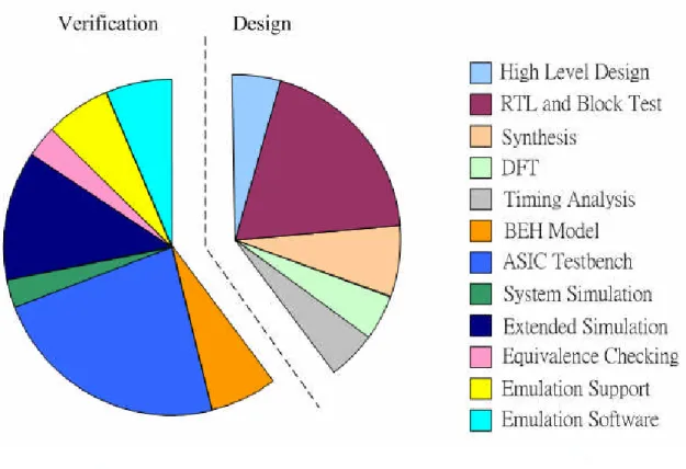
shown in Figure 1, verification takes 60%~80% of the overall design effort.[8] Nowadays, the
design bottleneck is verification. To implement a system at higher abstraction level can
increase the design productivity. If we want to improve the design productivity, we must
improve the verification methodology. In this point of view, the efficient simulation platform
is an important role in SoC design.
Figure 1 Breakdown of the Design Effort.
The purpose of this thesis is to implement a behavior model with error detection and error
correction functions on an electronic system level simulation platform and facilitate the
verification efficiency by hardware modeling technology.
important issue in communication system development. From a study by the Collett
International Research in 2000, the functional error is the most significant defect in SoC
design as shown in Figure 2.[21] It is necessary to find out all defects before type out the real
chip in order to avoid the expansive penalty of re-spin. Because the simulation platform
provides a heterogeneous simulation environment, the behavior model with hardware
accelerator in this system can be verified before the real RTL model is ready. In this way, the
development of hardware and software can be started concurrently. The high level
co-simulation affects the design efficiency obviously. Take WiMAX for example, it must be
more complicated than any former one. Because the proper design methodology is adopted,
the design and verification schedule will be shortened and the overall productivity will be
increased significantly.
1.3 The Focus of Our Work
In order to verify the behavior between the transmitter and the receiver, we implement a
virtual socket for packet transmission. This behavior model is used to deal with packet
transmission without physical connections and the socket API for network communication.
We also implement this virtual socket with error detection and error correction functions for
supporting data integrity. We demonstrate the functional verification at electronic system
level on the ARM-based platform. In order to decease the simulation time, we turn the CRC
function into hardware module for improving the simulation performance.
1.4 Brief in WiMAX
WiMAX (Worldwide Interoperability of Microwave Access) is a wireless Internet service
designed to cover wide geographical areas serving large numbers of users at low cost.
WiMAX is the synonym given to the IEEE 802.16 standard defining wide area wireless data
networking. WiMAX is the standard being adopted worldwide by manufacturers to insure
inter-operability of equipment. WiMAX is considered one of the best solutions for "last mile"
distribution. In contrast, wireless local area networks are designed to provide network access
within an office environment or a home once Internet service has been delivered to that point.
barrier in wireless wideband access. It can provide as high as 75Mbps data rate in a 20MHz
bandwidth. OFDM and OFDMA are kernel physical layer technique of WiMAX. OFDM is a
multi-carrier modulation technology and has already been applied in ADSL and WLAN.
OFDMA is an OFDM multiple access scheme that used in uplink. Each user is allocated
different sub-carriers and thus is distinguished by orthogonal sub-carriers.[17]
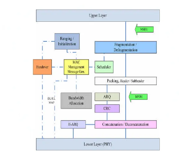
Figure 3 WiMAX MAC Architecture.
The functional blocks in the system architecture are shown in Figure 3. The system is
partitioned to two parts - the data plane and the control plane. The MAC data plane functions
and cyclic redundancy check, etc. The MAC control plane functionality, including system
control, can be implemented as a finite state machine in software or hardware.
1.5 Organization
The remainder of this thesis is organized as follows. In chapter 2, we describe the related
works and design concepts in our design. The virtual socket concept for packet transmission
in downlink and uplink are illustrated. In chapter 3, we illustrate the design process step by
step. Besides we demonstrate the heterogeneous simulation at electronic system level. A
hardware modeling technology is adopted in our design and we present the simulation
performance will be improved by hardware modeling technology. In chapter 4, we conclude
Chapter 2
Related Work
In this chapter, we explain some related works and design concepts about our design. In
order to explain why we implement our behavior model on ARM-based platform at electronic
system level, we discuss the SoC design and verification issues in section 2.1. The MAC
functions that are relative to our behavior model are explored in section 2.2. Different design
and verification languages are used for different purposes at different abstraction levels. In
section 2.3 the hardware modeling technology is discussed and SystemC language for
developing the hardware model in our design is introduced. In the section 2.4, the
platform-based design concept is explored and the actual implementation is demonstrated. In
the section 2.5, we propose a virtual socket concept for the packet transmission. We explain
the concept and the behavior of this model. Finally we make a summary of this chapter in
2.1 SoC Design and Verification Issue
As the semiconductor industry continues to drive toward more advanced manufacturing
technologies, all design companies face shrinking product lifecycles and rising demand for
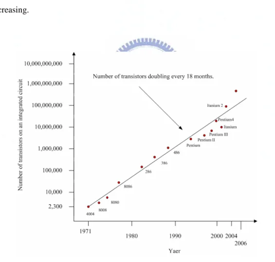
greater functionality. Moore’s Law is the empirical observation made in 1965 that the number
of transistors on an integrated circuit for minimum component cost doubles every 18 months,
as shown in Figure 4.[23] Due to the scale down of the transistor, the capacity in each device
is increasing.
Figure 4 Moore’s Law.
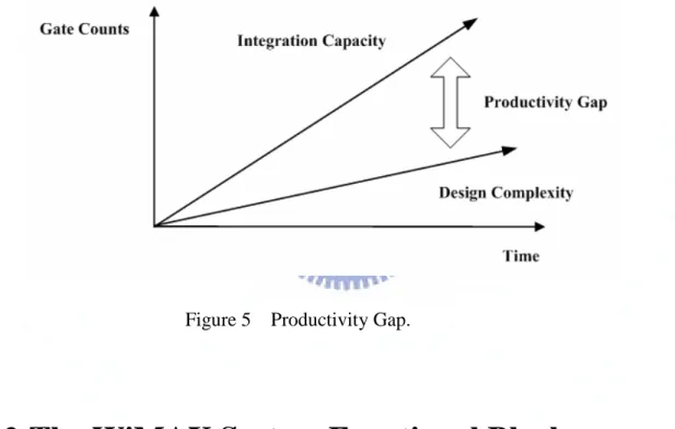
complexity. It means the growth of silicon complexity is much more than the designer’s
productivity. Therefore the productivity gap between integration capacity and design
complexity becomes worse as shown in Figure 5. In the SoC design, many design flows and
design methodologies are proposed to close the productivity gap like the platform-based
design and electronic system level design. We adopt both two design methodologies for our
development. We use the top-down design flow to design our communication system.
Figure 5 Productivity Gap.
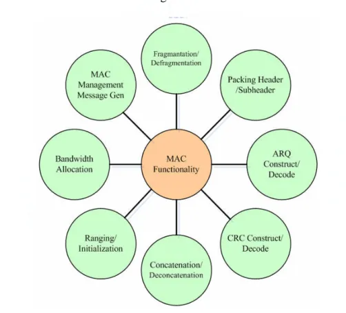
2.2 The WiMAX System Functional Block
In this subsection, we disclose the basic functions of WiMAX system. The MAC
management message generator is responsible to generate the corresponding message types in
specific communication situations. The cyclic redundancy check is responsible for error
support mobile user, the handover function must decide to link with a new base station and
disconnect with the current base station at proper moment. The scheduler is in charge of the
QoS control. Ranging and initialization is responsible for keeping the radio link working, like
synchronization, power control, etc. Packing, fragmentation, concatenation is responsible for
the transmission efficiency by constructing different packet sizes. Bandwidth allocation is
responsible for allocating the proper bandwidth when the subscribers request for bandwidths.
The breakdown of MAC functionality is shown in Figure 6. Detailed definition for each
related function is described in the following section.
2.2.1 MAC Management Message
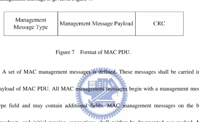
A MAC protocol data unit (PDU) consists of a fixed length header, a variable length
payload and an optional field for cyclic redundancy check (CRC). The format of the
management message is given in Figure 7.
Figure 7 Format of MAC PDU.
A set of MAC management messages is defined. These messages shall be carried in the
payload of MAC PDU. All MAC management messages begin with a management message
type field and may contain additional fields. MAC management messages on the basic,
broadcast, and initial ranging connections shall neither be fragmented nor packed. MAC
management messages on the primary management connection may be packed and/or
fragmented. For the SCa, OFDM, and OFDMA PHY layers, management messages carried
on the initial ranging, broadcast, basic, and primary management connections shall have CRC
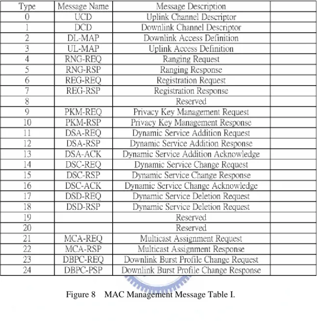
usage enabled. The encoding of the management message type field is given in Figure 8 and
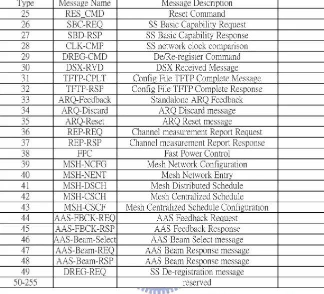
Figure 9 MAC Management Message Table II.
2.2.2 Header and Subheader
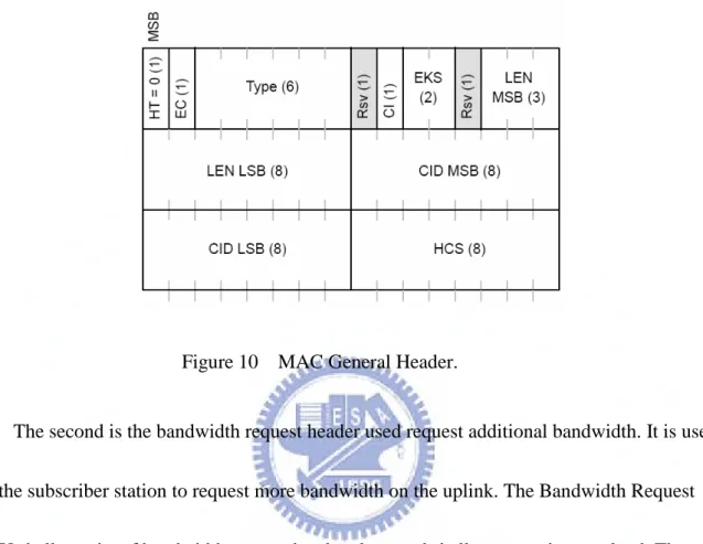
Two MAC header format are defined. The first is the generic MAC header that begins each
MAC PDU containing either MAC management messages or data from the upper layer. The
second is the bandwidth request header used to request additional bandwidth. The single-bit
formats. The HT field shall be set to zero for the Generic Header and one for a bandwidth
request header. The Figure 10 shows the format of MAC general header.[1]
Figure 10 MAC General Header.
The second is the bandwidth request header used request additional bandwidth. It is used
by the subscriber station to request more bandwidth on the uplink. The Bandwidth Request
PDU shall consist of bandwidth request header alone and shall not contain a payload. The
Figure 11 shows the format of the MAC bandwidth request header.[1]
There are five types of subheaders. The subheaders may be inserted in MAC PDUs
immediately following the generic MAC header. The definition of the type field is indicated
in Figure 12. The grant management subheader is used to convey bandwidth management
needs to the BS. The fragmentation subheader indicates the presence and orientation of
service data units (SDU) in the payload. The packing subheader indicates the packing of
multiple SDUs into signal PDU. If both the fragmentation subheader and grant management
subheader are indicated, the grant management subheader shall come first. The packing and
fragmentation subheaders are mutually exclusive and shall not both be present within the
same MAC PDU. The mesh subheader is only necessary for mesh network. All the
subheaders included the mesh subheader are within payload. If the mesh subheader is
indicated, it shall precede all other subheaders. The fast-feedback allocation subheader shall
always appear as the last per-PDU subheader. This is used to tell the PHY layer to provide an
immediate measurement of the quality of the radio signal.[1]
2.2.3 Automatic Repeat Request
The ARQ mechanism is a part of MAC, which is optional for implementation. When
implemented, ARQ may be enabled on a per-connection basis. The per-connection ARQ shall
be specified and negotiated during connection creation. A connection cannot have a mixture
of ARQ and non-ARQ traffic. Similar to other properties of the MAC protocol the scope of a
specific instance of ARQ is limited to one unidirectional connection. For ARQ-enabled
connections, enabling of fragmentation is optional. When fragmentation is enabled, the
transmitter may partition each SDU into fragments for separate transmission based on the
value of the ARQ_BLOCK_SIZE parameter. When fragmentation is not enabled, the
connection shall be managed as if fragmentation was enabled. In this case, regardless of the
negotiated block size, each fragment formed for transmission shall contain all the blocks of
data associated with the parent SDU. The ARQ feedback information can be sent as a
standalone MAC management message on the appropriate basic management connection, or
piggybacked on an existing connection. ARQ feedback cannot be fragmented.[1]
2.2.4 Cyclic Redundancy Check
The cyclic redundancy check (CRC) is a way to detect small changes in blocks of data.
stored, because an error of even one bit is often sufficient to make a system shutdown. An
error correction protocol triggered by CRC error detection can provide this accuracy at low
cost.
The CRC algorithm operates on a block of data as a unit. We can understand the CRC
better if we see a block of data as a single numerical value. The CRC algorithm divides this
large value by a magic number (the CRC polynomial or generator polynomial), leaving the
remainder, which is our CRC result.
The CRC result can be sent or stored along with the original data. According to the format
of PDU, we attach the CRC result to the tailor of payload. When the data is received, the CRC
algorithm can be reapplied, and the latest result compared to the original result. If any error
has occurred, we will probably get a different CRC result. Most uses of CRC do not attempt
to classify or locate the error, but simply arrange to repeat the data operation until no errors
are detected.
2.3 Design and Verification Language
Different design languages are used for different abstraction levels. The higher abstraction
level is suitable for algorithm development. On the other hand, the lower abstraction level is
design languages. Different design languages are for different purposes. The Matlab is a
powerful mathematic tool and it is used to model the complicated mathematic issues or
advanced algorithms. The hardware description language (HDL) like VHDL or Verilog is
used to model the real hardware behavior and evaluate the physical information like timing,
area, and power.
Figure 13 Different Levels of Abstraction.
In our implementation, we adopt C language and SystemC language to construct our
behavior model. C language is most popular language in the world and supported by various
compliers. It can be ported from one platform to another platform easily, so C language is
verification engineers and implementation engineers. In the following two subsections, we
explore the hardware modeling technology and introduce SystemC language. Our purpose is
to implement the behavior model at electronic system level and execute the heterogeneous
simulation, so both C language and SystemC language are necessary for the development of
our model.
2.3.1 Hardware Modeling
In the early 1980s, the logic of integrated circuits was designed via gate level drawing. The
appearance of the first IEEE HDL standard was in 1987. The hardware description languages
are meant to provide a unified notation for describing electronic systems at register transfer
level. In RTL design, a circuit behavior is defined in terms of the flow of signals or the
transfer of data between registers so the design efficiency is better than the gate level design.
SystemC was announced in 1999. It is a much higher level of abstraction than writing
hardware description language at register transfer level.
There are many differences between traditional and modern design processes. The main
advantage in the modern process is to enable both software and hardware development
concurrently. In order to start the software development and verification prior to the hardware
only shortens the SoC development schedule but also improves the simulation performance at
electronic system level platform. In our behavior model, we compare the performance
between the pure software version and the new version with hardware modeling. After the
simulation, we prove the hardware CRC module can improve the simulation performance.
2.3.2 SystemC
The first version of SystemC was released in September 1999. Early development was done
by Synopsys, UC Irvine and CoWare. The Open SystemC Initiative (OSCI) was founded in
2000. SystemC becomes one IEEE standard in 2005.
As a standard, SystemC could possibly enable and accelerate the exchange of system level
intellectual property (IP) models and executable specifications using a common C-based
modeling platform. SystemC provides a single language to define hardware and software
components, to facilitate hardware/software co-simulation, and to facilitate step by step
refinement of a system design down to the register transfer level for synthesis.
Replacing the traditional hardware description language (DHL) with SystemC minimizes
the communication overheads involved in current system design flow, deceases simulation
time and thus speeds up the design process.[12]
[14][15]. The first is it enables modeling of systems above the RTL level of abstraction –
including systems that might be implemented in hardware, software or a combination of both.
The second is SystemC promotes reuse of the developed components from one system to
another with minimum efforts. The third is SystemC offers good design space exploration of
functional specification and architectural implementation alternatives. The Figure 14 shows
the architecture of SystemC language.[24]
Figure 14 SystemC Language Architecture.
2.4 Platform-based Design
Our behavior model is implemented according to the platform-based design methodology.
time-to-market, design and manufacturing costs. The modern SoC design flow increases the
productivity of each engineer. Usually the engineers just change few functions in the former
design to create a new one. Most design effort is reused and shared in the following projects.
The engineers will reuse the components like the ARM processor, the memory, and some
peripheral modules. As shown in Figure 15, the AMBA interface and protocol enable the
designer to develop the SoC system by assembling essential IPs. The platform-based design
concept is adopted by our design methodology. In the following subsections, we will
introduce the features of AMBA, the interaction of hardware and software, and the memory
mapping concept for accessing declared registers.
Figure 15 The Platform-based Design.
2.4.1 AMBA
for the interconnection and management of functional blocks that makes up a System-on-Chip
(SoC). The AMBA protocol enhances a reusable design methodology by defining a common
backbone for SoC modules.
There are three different buses in the AMBA specification: AHB, ASB and APB. AHB
stands for Advanced High-performance Bus. AHB is a new generation of AMBA bus which
is intended to address the requirements of high-performance synthesizable designs. It is a
high-performance system bus that supports multiple bus masters and provides high-bandwidth
operation. ASB stands for Advanced System Bus. This is an older version has been replaced
by AHB. APB stands for Advanced Peripheral Bus. It is a simple lower performance and low
power bus used for low speed peripherals. The APB is optimized for minimal power
consumption and reduced interface complexity. The macrocells designed to interface with
AMBA can be seen as building blocks which can be reused in future designs and mixed and
matched in different combinations to realize complex systems in a shorter period of time. The
Figure 16 The AMBA Architecture.
2.4.2 The HW/SW Interaction
Hardware/software interaction plays an important role in co-design of the embedded system.
It connects the software part and the hardware part in a system. There are two main
approaches for hardware/software interaction: Polling and Interrupt.
Polling the device usually means reading its status register so often until the device's status
changes to indicate that it has completed the request. Interrupt is a signal from a device
attached to a processor or from a program within the processor that causes the main program
that operates the system to stop and figure out what to do next. An interrupt can be generated
by one of two sources: software interrupt and hardware interrupt. The interrupt signals
external device. These are called hardware interrupts. When a program receives an interrupt
signal, it takes a specified action. Interrupt signals can cause a program to suspend itself
temporarily to service the interrupt.
Figure 17 Interaction between Hardware and Software.
The behavior of the interrupt and the actual layout is shown in the Figure 17. The
interaction between our hardware module and ARM processor is hardware interrupt. This is a
more effective approach than polling. After the unprocessed data is moved into the input
buffer, the CRC module is enabled by software with the CRC_enable signal. Then the CRC
hardware module will start to process the data and return the CRC result. After the CRC
hardware finishing it job, the hardware module will inform the ARM core to fetch the CRC
result from the output buffer by using the interrupt signal. In the embedded system design, the
hardware module and jumps to the address of the service routine and deal with the process.
2.4.3 Hardware Registers
In embedded system design, hardware registers compose a storage area for control signals
and data.Hardware registers are contained within a certain peripheral unit. Usually we divide
the hardware registers into three types -- control registers, status registers, and data buffers. A
status register is a collection of bits for a processor that indicates the status of various specific
operations. When a status register is read, it will report the state of the peripheral device.
When a control register is written, it will change the state of the peripheral device. The data
buffers usually storage the raw data for processing and the output data for accessing. Registers
is costly, so the registers will not be used unlimited.
2.4.4 Memory Mapping
Memory mapping is a process that a digital hardware is connected to a processor’s address
bus and data bus. In this way, the component can be accessed exactly as if it were a memory
cell. To a processor, everything is memory. The memory mapping is to define the address of
the I/O registers in the memory table so the embedded processor can exactly access the
complementary methods of performing input/output between the CPU and I/O devices in an
embedded system. In our implementation, we use the memory-mapped I/O methodology.
Memory-mapped I/O uses the same bus to address both memory and I/O devices, and the
same CPU instructions are used to access both memory and I/O devices. The I/O devices
monitor the CPU's address bus and map the address to their hardware registers. The Figure 18
shows the memory map in our implementation.
2.5 Virtual Socket Concept
A socket is one end-point of a two-way communication link between two programs running
on the network. Socket classes are used to represent the connection between a client program
and a server program. In our simulation platform, we don’t have the socket API for
communication, so we propose the virtual socket concept for our simulation platform. In the
simulation platform, we use share memory as the transmission medium. Besides we define an
arbiter, some control flags, and a finite state machine for synchronizing the data transmission.
2.5.1 Simulation Platform and Architecture
SoC Designer is a system level simulation tool supporting the hardware modeling in
SystemC. New SystemC components can be created using the SoC Designer Component
Wizard. For legacy SystemC TLM model reuse, existing SystemC models can be imported
into SoC Designer with little or no modifications to the original source code. There are two
different methods for importing SystemC models into SoC Designer environment: one can
use a SoC Designer component as a top level wrapper to instantiate the modules as
sub-components, or one can import a module directly without a wrapper by changing the
module to inherit from a special base class provided in SoC Designer.[20] The Figure 19
level model to accelerate the simulation speed.
Figure 19 The Architecture of Simulation Platform.
2.5.2 Downlink and Uplink Procedure
The ESL simulation platform can support the multi-cores simulation. Take advantage of
this characteristic, we can model the behavior of the transmitter and the receiver with the
virtual socket. Furthermore, we build a traffic model for the uplink and downlink traffic, so
the interaction between different members becomes possible. Besides developing the
transmitter and the receiver, we build an error model to present the channel fading. In order to
synchronize these components in this platform, we defined a finite state machine to
components in this simulation environment.
In the left side of Figure 20 shows the downlink traffic behavior. In the beginning, the base
station will generate the packets and transmit these packets to the subscriber station.
According to the specification, the base station will generate the CRC result and attach to the
tailor of the packet. It is used for error detection in the unstable wireless environment. In the
TX State of base station, we write the packet into the RX buffer. The channel runs a program
and presents an error probability on the air. The error model of the channel will decide to
change the value in the RX buffer or not according to a random number. In the RX state of the
subscriber station, the subscriber station will receive the packet in the RX buffer, compare the
CRC result and inform the transmitter to transmit the next packet or retransmit the original
one.
In the right side of Figure 20 shows the behavior of uplink traffic. The subscriber station
will generate the ARQ frame to inform the base station the outcome of the transmission. In
the TX state of the subscriber station, the subscriber station will transmit the ARQ frame
according to the CRC check result and write the ARQ packet into the TX buffer. In the TX
state of the base station, the base station will receive the packet, decode the packet and decide
Figure 20 Downlink and Uplink Procedure
2.6 Summary
In this chapter, we introduce the design concepts for our behavior model. In the section 2.1,
we discuss the SoC design and verification issues. In the section 2.2, we identify some
subfunctions which are relative to our implementation. In the section 2.3, we explore the
abstraction level of our implementation and choose the proper design language to model our
design. In the section 2.4, we illustrate the concept of platform-based design, the embedded
system design and the details for hardware modeling. In the section 2.5, we introduce the
Chapter 3
Case Study:A Behavior Model Design
The related work about our implementation is described in the previous chapter. In this
chapter, we describe the development of our behavior model and demonstrate the simulation
result. In the beginning, we develop and verify our reference software and applications in C
language on the personal computer environment. Then we port our C model to the ESL
platform and verify the functionality of the traffic behavior, the error detection behavior, and
the error correction behavior. Further, we implement a hardware module for
hardware/software co-simulation platform. We modify the firmware to define the interaction
between the hardware module and the processor.
3.1 Our Design Flow for Behavior Model
We implement our behavior model in C code according to the IEEE 802.16 specification.
The specification describes the MAC functionality in English. When we study the meanings
executable code in C language. The executable specification not only avoids the ambiguous
meaning in nature language but also provides the quantitative analysis in engineering
applications. After verifying on PC, we use the ADS (ARM Developer Suite) tool to generate
the image file and download to the SoC Designer for simulation. Then we design a hardware
module for CRC function and compare the simulation performance with the pure software
verison. The Figure 21 shows the design flow and the development environments for our
behavior model.
3.1.1 Reference Software Development
The basic function of our behavior model is to provide data integrity during the
transmission. There are three subsystems are built in our implementation – the BS module, the
MS module, and the Channel module. The transmission side generates the transmitted packets
based on the proper format and generates the CRC result for the error detection. The channel
models the behavior of channel fading and changes the value in the RX buffer. The channel
also acts like the arbiter to schedule the TX/RX behavior by changing the control flags and
the state of finite state machine. The received side generates the CRC result again and
compares the CRC value to confirm the completeness of received packet. According to the
comparison, the receiver generates the ACK message to inform the transmitter to transmit the
next packet or retransmit the original one.
Figure 22 The Function for Error Detection and ARQ Frame Generation.
Some control flags and data buffers are used in the transmission behavior, most of the
detection function and the retransmission scheme on the PC platform as shown in Figure 22.
Furthermore we implement a basic protocol for TX/RX transmission. Stop and wait
transmission is the simplest reliability technique and is adequate to a very simple
communications environment. A stop and wait protocol transmits a Protocol Data Unit (PDU)
of information and then waits for a response. The receiver receives each PDU and sends an
acknowledgement (ACK) PDU if a data PDU is received correctly, and a negative
acknowledgement (NACK) PDU if the data was not received correctly. The Figure 23 shows
the behavior of transmission.
3.1.2 Simulation on ADS and ESL Platform
When we verify the communication system, we need to create the environment for
communication under the conditions that no physical layer and no socket API are existed. We
establish the logic architecture, which is shown in the Figure 24. We divide our C model to
three subsystems – the BS module, the MS module, and the Channel model.
The design concept of the communication system is different from the other systems like
various multi-media decoders. Communication systems must communicate with the other
members in the wireless environment. Usually it is hard to build the whole system and verify
the protocol in the beginning. In our simulation platform, the SoC designer supports the
multi-core simulation. It means different programs can be executed concurrently on this
platform. We take advantage of the simulation platform and construct a logic system on it
including the base station, the subscriber station, and the channel model to verify the
downlink and uplink traffic.
When developing exactable codes for three ARM processors, we use ARM Developer Suite
(ADS) to generate the three image files. After passing the debugging in the ARM compiler,
linker, and utility programs proved by ADS, we load the image codes to three subsystems on
Figure 24 The Logic and Physical System Architecture.
3.1.3 System Level Simulation with Pure Software
The Figure 25 shows the functional verification on the ESL platform. The simulation
demonstrates the interaction between the base station and the subscriber station on the
downlink traffic and the uplink traffic. The simulation also demonstrates the error model to
replace the real wireless channel because there are no physical connection and actual medium.
This simulation also demonstrates the error detection and error correction function in a
Figure 25 The Functional Verification.
3.2 Our Design Flow for Hardware Modeling
In this section we explore our design flow for hardware modeling. The design process
includes the interface design, I/O register design, behavior model coding, and firmware
coding. The Figure 26 shows the design flow and the development environments for our
hardware modeling. In the research [16] [18] indicate the framing function, ARQ function, the
encryption function, and the CRC function are timing critical and large overhead. Among
Figure 26 Design Flow for Hardware Modeling
3.2.1 Interface Design
There are three main interfaces in our hardware module. One is the AMBA for transferring
the transmitted packet and fetching the CRC result. Another is the interrupt signal for
indicating the processor that the CRC result is ready. The third is the input pin of clock cycle.
Figure 27 Interface Design
3.2.2 Input/Output Register Design
Within the hardware module we define input registers, output registers, and data buffers.
The CRC_enable, BytesOffset, and Input_Buffer are input ports. The CRC_done and
CRC_result are the output ports. The processor moves the unprocessed data to the
Input_Buffer and defines the length of unprocessed data by setting the CRC_length. The
processor enables CRC hardware module by setting the CRC_enable equal to “high”. After
calculating, the CRC result will be written into the Output_Buffer. Then CRC_done register
will be set to “high” and this signal is wired to the processor for informing the processor that
Figure 28 I/O Register Design
3.2.3 Behavior Model Coding
New SystemC components can be created by using the SoC Designer Component Wizard.
We use a SoC Designer component as a top level wrapper to instantiate the modules as
sub-components. The component wizard will generate the following files: A cpp/h file for the
SoC Designer component, a cpp/h file for each slave port, and a cpp/h file MxDI if
selected.[20] The newly generated SoC Designer component does not contain any behavior
and we have to construct the CRC function in Visual C++ environment. Then we generate a
library with correct behavior. The design is based on the SystemC language. It can facilitate
3.2.4 Import to the ARM-based Platform
We imported the SystemC component and connected the interfaces properly to the ralative
SoC Designer modules. In general, ports and channels of imported SystemC modules are
based on user-defined SystemC interfaces. We drag the CRC module from the component
window and connect the module to the AMBA bus and the interrupt controller.
3.2.5 System Level Simulation with Hardware Modeling
After we establish the SystemC model, we can fast prototype the hardware model in
SystemC at higher abstraction level. This is good for designers to verify the system
functionality concurrently by both the hardware side and the software side. This also can
reduce the rework penalty and the delay in a rush schedule.
As the Figure 29 shown, the simulation result demonstrates the hardware/software
heterogeneous simulation on SoC Designer platform. The completed module can be defined
Figure 29 The SoC Designer Co-simulation Environment.
3.3 Simulation Result and Application
There are two purposes for the hardware/software co-simulation. The first is we want to
guarantee that the hardware module behavior is correct. The second is we want to improve the
simulation performance at electronic system level.
3.3.1 Hardware/Software Co-verification
In this subsection, we demonstrate the functional verification of hardware and software
socket for packet transmission and guarantees the data integrity in a channel with an error
model. The behavior model is implemented on the ARM-based platform. It can be used to
design the other embedded communication systems. Due to the higher abstraction level, the
simulation overhead is less than the register transfer level. Furthermore, the simulation
platform supports the hardware/software co-verification. We turn the CRC function into
hardware module in SystemC language. Hardware/software co-verification is to make sure the
embedded software works correctly with the hardware parts. The design methodology
accelerates the firmware debugging. Early debugging also reduces the risk of redesign.
3.3.2 Simulation Model and Simulation Result
In this subsection, we use three simulation models to compare the simulation performance.
We want to calculate the clock cycle of the software function and hardware module based on
different packet sizes. There are three simulation models - the model with no CRC function,
the model with software CRC function, and the model with hardware CRC module. The
Figure 30 shows the clock cycles of three simulation models in three different packet sizes.
The Figure 31 shows the comparison of simulation result. We obtain the clock cycle for
software function and hardware module in different transmitted packet sizes. The simulation
result explains the improvement of the overall system performance in heavy traffic data. The
simulation shows that there are 1.6% and 11.7% improvements by setting the packet size in
100bits and 1000bits respectively.
0 5000000 10000000 15000000 20000000 25000000 30000000 without CRC wit h SW CRC wit h HW CRC wit hout CRC wit h SW CRC with HW CRC wit hout CRC wit h SW CRC wit h HW CRC Function C lo c k C y c le 10(bits) 100(bits) 1000(bits)
Figure 31 The Simulation Result
The processed data is transferred between software and hardware through the AMBA bus.
The bus transaction is an overhead for system simulation. For the small packet size, the
simulation result of hardware version is worst because the extra overhead in bus transaction is
transaction is smaller than the processing gain of hardware component. The packet size in
100bits is an approximate threshold in our behavior model for using the CRC accelerator.
3.4 Summary
In this chapter, we illustrate our implementation process and demonstrate our simulation
results. In the section 3.1, we explore our design flow for our behavior model and finish the
system level simulation. In the section 3.2, we explore our design flow for hardware modeling
and finish the heterogeneous simulation. In the section 3.3, we have a comparison between the
pure software version and the other version with hardware accelerator model. The design
methodology and platform can be used to verify different communication scenarios. By using
this platform, a behavior model with the error detection and error correction function is
demonstrated in this chapter. The simulation result shows our hardware accelerator can
Chapter 4
Conclusions and Future Work
This thesis presents an implementation of our behavior model on an electronic system level
simulation platform to enable the data transmission. A virtual socket concept is proposed to
deal with the packet transmission. We implement our behavior model at the electronic system
level simulation platform, which provides three purposes: system level design, system level
verification, and hardware/software co-design. The design concepts and design methodology
are exploded. This behavior model demonstrates the packet transmission between the
transmitter and the receiver and guarantees the data integrity. The behavior model also can be
used to verify the different communication scenarios.
The heterogeneous simulation improves the efficiency of the system simulation. The
hardware module is become a library that can be reuse for the other designs. Finally, we
demonstrate the heterogeneous simulation at electronic system level and improve the efficient
for the system simulation.
For the further improvement of our behavior model, the hardware module can be realized in
Bibliography
[1] IEEE 802.16.IEEE Standard for Local and Metropolitan Area Networks-Part 16.Air Interface for Fixed Broadband Wireless Access Systems-2004.
[2] A. Ghosh et al., “Broadband Wireless Access with WiMAX/802.16:Current Performance Benchmarks and Future Potential”, IEEE Communications Magazine, vol.43, no.2, pp. 129-136, 2005.
[3] Thorsten Grotker, Stan Liao, Grant Martin and Stuart Swan, System Design with SystemC, Kluwer Academic Publisher, 2002.
[4] M. Keating and P. Bricaudr, Reuse Methodology Manual for System-On-A-Chip Designs, Kluwer Academic Publishers, 2002.
[5] Steve Furber, ARM System-on-Chip Architecture second edition, ADDISON WESLEY, 2000.
[6] Takayuki Tachikawa and Makoto Takizawa, “ARQ Protocols for Bi-directional Data Transmission”, International Conference on Information Networking (ICOIN-12), Tokyo, Japan, pp.468-473, 1998.
[7] Tim Hopes, “Hardware/Software Co-verification, an IP Vendors Viewpoint”, Proceedings of the International Conference on Computer Design (ICCD), Austin, TX, USA, pp.242-246, 1998.
[8] Jing-Yang Chou, “Special Topics in Computer Aided Design”.
[9] Theo A.C.M Claasen, “An Industry Perspective on Current and Future State of the Art in System-on-Chip (SoC) Technology ” Proceedings of the IEEE, Vol. 94, No. 6, pp. 1121-1137, 2006.
[11] Ray Turner, “System Level Verification – a Comparison of Approaches”, Proceedings of the 10th IEEE International Workshop on Rapid System Prototyping, Clearwater, FL, USA, pp154-159, 1999.
[12] Joanne DeGroat, Arun Raman, Bakr Younis, “A Design Project for System Design with SystemC”, Proceedings of the IEEE International Conference on Microelectronic Systems Education, Anaheim, CA, USA, pp108-109, 2003.
[13] Liao, S. Y., “Towards a New Standard for System-Level Design”, Proceedings of the Eighth International Workshop on Hardware/Software Co-design, San Diego, 2000.
[14] Open SystemC Initiative. See http://www.systemc.org
[15] J. Bhasker, A SystemC Primer, Star Galaxy Publishing, 2002.
[16] H. Holisaz, S. Shamshiri et al, “Hardware Accelerator IP-Core for Wireless 802.16 MAC”, IFIP International Conference on Wireless and Optical Communication Networks, Bangalore, India, 2006.
[17] Liangshan Ma and Dongyan Jia, “The Competition and Cooperation of WiMAX, WLAN and 3G”, 2nd Asia Pacific Conference on Mobile technology application and systems, Guangzhou, China, 2005.
[18] Nak Woon Sung, “HW/SW Codesigned Implementation of IEEE 802.16 TDMA MAC for the Subscriber Station”, Proceedings of the Fourth Annual ACIS International Conference on Computer and International Science, Jeju Island, South Korea, pp436-440, 2005.
[19] Jorg Henkel, “Closing the SoC Design Gap”, Computer, Volume 36, Issue 9, pp119-121, 2003.
[20] ARM Limited, “RealView SoC Designer SystemC-TML Import”, version 3.06, pp. 22, 2006.
[21] Collett International Research:2000, 2002 Functional Verification Studies.
[22] ARM Limited, “AMBA Specification (Rev 2.0)”, pp. 1-4, 1999.
[23] Gordon Moore, “Cramming more components onto integrated circuits”, Electron. Mag, vol.38, no.8, pp.114-117, 1965.
[24] Thorsten Grotler, Stan Liao, Grant Martin, Stuart Swan, System Design with SystemC, Kluwer Academic Publishers, 2002.
[25] International Technology Roadmap for Semiconductors, 2006 Update, Semiconductor Industry Association. Available from http://www.itrs.net/