使用砷化銦鎵假型高速電子移動電晶體之單晶毫米波倍頻器及新式寬頻開關之設計
80
0
0
全文
(2) 使用砷化銦鎵假型高速電子移動電晶體之 單晶毫米波倍頻器及新式寬頻開關之設計 Design of Millimeter-wave Frequency Doubler and New Broadband Switches using InGaAs pHEMT. 研 究 生:陳揚裕. Student:Yang-Yu Chen. 指導教授:鍾世忠 博士. Advisor:Dr. Shyh-Jong Chung. 國 立 交 通 大 學 電 信 工 程 學 系 碩 士 班 碩 士 論 文. A Thesis Submitted to Institute of Communication engineering College of Electrical Engineering and Computer Science National Chiao Tung University in Partial Fulfillment of the Requirements For the Degree of Master of Science in Communication Engineering June 2004 HsinChu, Taiwan, Republic of China 中華民國 九十三 年 六 月.
(3) 使用砷化銦鎵假型高速電子移動電晶體之 單晶毫米波倍頻器及新式寬頻開關之設計. 研 究 生:陳揚裕. 指導教授:鍾世忠 博士. 國立交通大學 電信工程學系碩士班. 摘要. 這篇論文中展示了使用砷化銦鎵假型高速電子移動電晶體之單晶毫米波的 兩種電路,包含一個 35 轉 70 GHz 的毫米波二倍頻器及兩個寬頻開關。首先, 仔細描述了倍頻器的設計方法,再利用 B 類的操作點去完成一個在輸入為 1 dBm 時有其最大的轉換增益為 -8.4dB 的 35 轉 70 GHz 之二倍頻器,此設計在其中心 頻率 35 GHz 附近有 1 GHz 左右的頻寬而且有著平坦的轉換增益。其次,也詳盡 的描述了寬頻毫米波開關的設計方法並且展示一個從 24 到 65 GHz 的單刀單擲 開關與一個從 30.5 到 64.5 GHz 的單刀雙擲開關之實例。24 到 65 GHz 的單刀單 擲開關之設計有小於 3dB 的介入損耗與大於 30dB 的隔絕度,在中心頻率為 44.5 GHz 處有 41 GHz 的頻寬與平坦的介入損耗。30.5 到 64.5 GHz 的單刀雙擲 開關有小於 6dB 的介入損耗與大於 30dB 的隔絕度,在中心頻率為 47 GHz 處 有 34 GHz 的頻寬與平坦的介入損耗。. I.
(4) Design of Millimeter-wave Frequency Doubler and New Broadband Switches using InGaAs pHEMT. Student:Yang-Yu Chen. Advisor:Dr. Shyh-Jong Chung. Institute of Communication engineering National Chiao Tung University. ABSTRACT. Two kinds of MMIC circuits using InGaAs pHEMT are exhibited in this thesis, including a 35-to-70 GHz millimeter-wave frequency doubler and two broadband switches. First, the design methodology of the frequency multiplier is fully described. The class B operation was employed to achieve the 35-to-70 GHz frequency doubler with measured maximally conversion gain of -8.4 dB for 1 dBm input power. This design has 1 GHz bandwidth centered at 35 GHz for a flat conversion gain. Secondly, the design methodology of broadband millimeter-wave switches is shown in detail, along with the demonstrations of a 24-to-65 GHz SPST switch and a 30.5-to-64.5 GHz SPDT switch. For the designed 24-to-65 GHz SPST switch, the measured insertion loss is less than 3 dB and the isolation is better than 30 dB. It has 41 GHz bandwidth centered at 44.5 GHz for a flat insertion loss. For the design of 30.5-to-64.5 GHz SPDT switch, the measured insertion loss is less than 6 dB and the isolation is better than 30 dB with a total bandwidth of 34 GHz centered at 47 GHz for a flat insertion loss. II.
(5) ACKNOWLEDGMENTS 本篇論文可以順利完成,首先要感謝我的指導教授鍾世忠博士,在我的研究 過程中提供了一個資源充足的實驗室,老師豐富的學識、待人處世的寬厚和對研 究上的執著與熱忱,不但使我在學識與修養方面更上一層樓,也讓我學會以更嚴 謹的態度面對浩瀚無涯的研究世界。同時要感謝口試委員瞿大雄教授、張志揚教 授及陳浩暉教授的不吝指導得以使此篇論文更為完善;此外,要特別感謝張教授 在V-BAND量測上所給予的協助。 其次,我要感謝實驗室的成員們,在這兩年之中對我的鼎力相助,實驗室助 理小正正(又正)在實驗室大小事務上的處理;經驗豐富的卓如學長在電路量測各 方面的支援及經驗分享;待人溫和親切的俊(俊甫)同學在課業、電路模擬量測與 晶片下線上的相互討論與協助,並有著一起共患難的珍貴情誼;樂天大方的凱爺 (凱得)同學在天線設計上的教導,並帶給實驗室無限的搞笑與歡樂,使研究的過 程中更為順暢無阻,實為功德一件;美麗漂亮楚楚動人的電波組組花暨偶極天線 女王王小雅(雅瑩)同學在專業的耦合諧振環的教學與親切歡愉的言談,更會讓我 有十分想到實驗室做研究的動力;微波之神阿全(信全)同學在功課及學術研究上 的相互切磋討論,讓我有更清楚的微波與天線設計的觀念;英俊瀟灑的小洲洲(明 洲)同學在低溫共燒陶瓷模組的專業與三不五時可以哈啦的功力,令我望塵莫 及,怎麼學都學不來;疑似黑社會老大的鄭小力(怡力)同學在天線專業與各種行 為上十分的有個性,讓實驗室的生活更增添了一份和諧快樂的氣氛;很有原則的 廖(伸憶)同學在日常生活和電路實作上的經驗與討論,讓研究更為之完整。再者 有實驗室的學弟妹們,活潑美麗的卡輪(珮如)、體育班班長小民(民仲)、聰明的 阿信(侑信)、親切的清文、和善的嘉祐和消失已久的學妹旻靜與慧文,謝謝你們 日常生活的關心與扶持,讓我的研究之路更為順暢。另外還有我的大學同學小牧 (牧榮)和小貓(禮鈞)與研究所同學金毛(書豪)、智閔和精王(明治),因為你們讓我 的生活更添加了許多色彩。並且特別感謝歐弟(雅婷)和若萸幫我做英文校稿。 最後,要感謝陪我一路走來的家人,你們的支持是我做研究最大的動力,謝 謝你們一直在我身邊陪伴我、鼓勵我,這一路走來你們辛苦了。僅以此篇小小的 論文獻給所有關心我的人,能夠劃上一道絢麗的彩虹,均是因為你們。. III.
(6) Table of Contents Abstract (Chinese) ..................................................................................................I Abstract (English) ..................................................................................................II Acknowledgments .................................................................................................III Table of Contents ..................................................................................................IV List of Tables ..........................................................................................................VI List of Figures .......................................................................................................VII. Chapter 1. Introduction. 1.1 Motivation ...........................................................................................................1 1.2 Organization ........................................................................................................2. Chapter 2. Design Methodology of Frequency Multiplier. 2.1 Overview ...… … … … … … … … … … … … … … … … … … … … … … ..… … … … 3 2.2 Nonlinear Devices ...… … … … … … … … … … … … … … … … … … ..… … … … ..3 2.3 Biasing Points Considerations … … ..… … … … … … … … … … … ..… … … … .… 4 2.3.1 Class A ......................................................................................................5 2.3.2 Class B ......................................................................................................6 2.3.3 Resistive Concept ..… … … … … … … … … … … … … … … … … … … .… ..7 2.4 Frequency Multiplier Design ..… … … … … … … … … … … … … … … … … … … 8 2.4.1 Architectures of Frequency Multipliers ..… ..… … … … … … … … … … ...8 2.4.2 Input and Output Matching Network Configurations ...… … … … … … ...9. Chapter 3. Frequency Multiplier using InGaAs pHEMT. 3.1 Overview ...… … … … … … … … … … … … … … … … … … … … … … … … … … 15 3.2 MMIC Foundry Description ...… … … … … … … … … … … … … … … … … … ...15 3.3 35-to-70 GHz Frequency Doubler using InGaAs pHEMT … … … .… … … … ..16 3.3.1 Circuit Design … … … … … … … … … … … … … … … … … … … … … … .16 3.3.2 Simulated Results ...… … … … … … … … … … … … … … … … … … … … 17 3.3.3 Measurement Considerations ...… … … … … … … … … … … … … … … ..18 3.3.4 Measured Results ...… … … … … … … … … … … … … … … … … … … … 19. Chapter 4. Design Methodology of Broadband Switches IV.
(7) 4.1 Overview ...… … … … … … … … … … … … … … … … … … … … … … … … … ....32 4.2 Switching Devices ...… … … … … … … … … … … … … … … … … … … … … ..… 32 4.3 Broadband Switch Design ...… … … … … … … … … … ..… … … … … … … .… ...34 4.3.1 Basic Switch Configurations ...… … … … … … … … … … … … … … … ...34 4.3.2 Single-Pole Single-Throw Switch ...… … … … … … … … … … … … … ...37 4.3.3 Single-Pole Double-Throw Switch … … … … … … … … … … … … … … 39 4.3.4 Single-Pole m-Throw Switch … … … … … … … … … … … … … … ..… ...40. Chapter 5. New Broadband Switches using InGaAs pHEMT. 5.1 Overview … … … … … … … … … … … … … … … … … … … … … … .… … … … ..47 5.2 MMIC Foundry Description ...… … … … … … … … … … … … … … … … … … ...47 5.3 24-to-65 GHz Single-Pole-Single-Throw Switch using InGaAs pHEMT … ....48 5.3.1 Circuit Design ...… … … … … … … … … … … … … … … … … … … … … ..48 5.3.2 Simulated Results ...… … … … … … … … … … … … … … … … … … … … 48 5.3.3 Measurement Considerations ...… … … … … … … … … … … … … … … ..49 5.3.4 Measured Results ...… … … … … … … … … … … … … … … … … … … … 50 5.4 30.5-to-64.5 GHz Single-Pole-Double-Throw Switch using InGaAs pHEMT 50 5.4.1 Circuit Design ...… … … … … … … … … … … … … … … … … … … … … .50 5.4.2 Simulated Results ....… … … … … … … … … … … … … … … … … … … ...51 5.4.3 Measurement Considerations ...… … … … … … … … … … … … … … … ..52 5.4.4 Measured Results ...… … … … … … … … … … … … … … … … … … … … 52. Chapter 6. Conclusions .........… … … … … … … … … … … … … … … … … ..64. References ...… … … … … … … … … … … … … … … … … … … … … … … … … … … 67. V.
(8) List of Tables Table 4.1 Tuned capacitor values for simulating a quarter-wavelength stub… … … 44 Table 4.2 Design tables for Mumford’s maximally flat stub filters… … … … … … ..45. VI.
(9) List of Figures Figure 2.1 The Schottky barrier diode (SBD) with (a) general structure, (b) its equivalent circuit… … … … … … ..… … … … … … … … … … … … … … ...10 Figure 2.2 The large-signal model of a FET… … … … … … … … … … … … … … … .10 Figure 2.3 DC characteristics of the FET. (a) Ids versus Vgs and Vds, (b) Ids and Gm versus Vgs at Vds = 1.5 V… … … … … … … … … … … … … … … … … … ..11 Figure 2.4 Class A operation with (a) small-signal, (b) large-signal… … … … … … .12 Figure 2.5 Class B operation.… ....… ..… .… … … … … … … … … … … … … … … … .13 Figure 2.6 The single-ended configuration of a frequency multiplier… … … … … ...13 Figure 2.7 The balanced configuration of a frequency multiplier… … … … … … … .14 Figure 2.8 The basic configuration of a frequency doubler… … … … … … … … … ..14 Figure 3.1. The schematic diagram of the 35-to-70 GHz frequency doubler… … … .21. Figure 3.2. Layout of the 35-to-70 GHz frequency doubler… … … … … … … … … ...21. Figure 3.3 The simulated conversion gain, 1f0 and 3f0 rejection versus input power of the 35-to-70 GHz frequency doubler… … … … … … … … .… .… ..… ..22 Figure 3.4 The simulated output power versus input power of the 35-to-70 GHz frequency doubler… … … … … … … … … … … … … … … … … … … … … 22 Figure 3.5 The simulated conversion gain, 1f0 and 3f0 rejection versus frequency of the 35-to-70 GHz frequency doubler at (a) Pin = 1dBm, (b) Pin = 6dBm… … … … … … … … … … … … … … … … … … … … … … … … … ...23 Figure 3.6 The simulated small-signal S-parameters of the 35-to-70 GHz frequency doubler. (a) From 20 to 50 GHz for S11 and S21, (b) from 60 to 80 GHz for S22… … … … … … … … … … … … … … … … … … … … … … … … … .24 Figure 3.7 The simulated large-signal S-parameters of the 35-to-70 GHz frequency doubler from 30 to 40 GHz for S11, S21 and S22… … … … … … … … ..25 Figure 3.8 Signal responses produced by a 76 GHz signal in W-band… … … … … .25 Figure 3.9 The test setups for the 35-to-70 GHz frequency doubler characterization. (a) Power measurement, (b) stability assurance… … … … … … … … … ..26 Figure 3.10 The microphotograph of the 35-to-70 GHz frequency doubler… … … .26 Figure 3.11. The measured conversion gain, 1f0 and 3f0 rejection versus input power of the 35-to-70 GHz frequency doubler… … … … … … … … … … … … 27. Figure 3.12 The measured output power versus input power of the 35-to-70 GHz frequency doubler… … … … … … … … … … … … … … … … … … … … ..27 VII.
(10) Figure 3.13 The simulated conversion gain, 1f0 and 3f0 rejection versus frequency of the 35-to-70 GHz frequency doubler at (a) Pin = 1dBm, (b) Pin = 6dBm… … … … … … … … … … … … … … … … … … … … … ...… … … ..28 Figure 3.14 The measured small-signal S-parameters of the 35-to-70 GHz frequency doubler. (a) From 20 to 50 GHz for S11 and S21, (b) from 75 to 80 GHz for S22… … … … … … … … … … … … … … … … … … … … … … ...29 Figure 3.15. Frequency spectrum from 58 to 75 GHz produced by a 70 GHz signal… … … … … … … … … … … … … … … … … … … … … … … … … … ...… … 30. Figure 3.16. Frequency spectrum from 75 to 110 GHz produced by a 105 GHz signal … … … … … … … … … … … … … … … … … … … … … … … … … … … ...30. Figure 3.17 (a) A 70 GHz real signal, (b) a 105 GHz real signal, (c) a 61.2 GHz spurious signal, (d) a 78.09 GHz spurious signal… … … … … … … … ..31 Figure 3.18. Frequency spectrum produced by a 35 GHz leakage signal, (a) from 0 to 40 GHz, (b) from 0 to 1 GHz...… .… .… .....… … .… … .… … … ..… ..… 31. Figure 4.1 (a) A general structure of the PIN diode, (b) ?-type, (c) p-type… … … ...41 Figure 4.2. Linear operational regions of a FET switch… … … … … … … … … … … .41. Figure 4.3 The FET in switching configuration… … … … … … … … … … … … … … 42 Figure 4.4. Complete equivalent circuit for, (a) low-impedance state, (b) high-impedance state… … … … … … … … … … … … … … … … … … … ...42. Figure 4.5. Simplified equivalent circuit for, (a) low-impedance state, (b) high-impedance state… … … … … … … … … … … … … … … … … … … ...42. Figure 4.6. Series-type switch configuration, (a) transmission line model, (b) equivalent circuit model… … … … … … … … … … … … … … … … … … ..42. Figure 4.7. Shunt-type switch configuration, (a) transmission line model, (b) equivalent circuit model… … … … … … … … … … … … … … … … … … ..43. Figure 4.8. Series-shunt switch configuration, (a) transmission line model, (b) equivalent circuit model… … … … … … … … … … … … … … … … … … ..43. Figure 4.9. Circuit model used for Fisher’s equivalent circuit… … … … … … … … ...44. Figure 4.10. Summary of Fisher’s method for simulating a quarter-wavelength stub with a capacitor and its parallel tuner… … … … … … … … … … … … … 44. Figure 4.11. Equivalent circuit for Mumford’s maximally flat stub filter design… ..44. Figure 4.12 Equivalent circuit for the transmission state of the SPST switch… … ..45 Figure 4.13 The SPDT switch with, (a) series-type configuration, (b) shunt-type configuration… … … … … … … … … … … … … … … … … … … … .… … 46 VIII.
(11) Figure 4.14 (a) SPDT switch implemented with Fisher’s method, (b) equivalent filter circuit for transmission state… … … … … … … … … … … … … … 46 Figure 5.1 The schematic diagram of the 24-to-65 GHz SPST switch… … … … … .54 Figure 5.2. Layout of the 24-to-65 GHz SPST switch… … … … … … … … … … … ...54. Figure 5.3 The simulated return loss and insertion loss for the on-state of the 24-to-65 GHz SPST switch… … … … … … … … … … … … … … … … … .55 Figure 5.4 The simulated return loss and isolation for the off-state of the 24-to-65 GHz SPST switch… … … … … … … … … … … … … … … … … … … … … 55 Figure 5.5 The simulated output power versus input power of the 24-to-65 GHz SPST switch… … … … … … … … … … … … … … … … … … … … … … .… 56 Figure 5.6 The test setups for the 24-to-65 GHz SPST switch characterization. (a) S parameter measurement, (b) P1dB at 38 GHz… … … … … … … … … … .56 Figure 5.7 The microphotograph of the 24-to-65 GHz SPST switch… … … … … … 57 Figure 5.8 The measured return loss and insertion loss for the on-state of the 24-to-65 GHz SPST switch… … … … … … … … … … … … … … … … … .57 Figure 5.9 The measured return loss and isolation for the off-state of the 24-to-65 GHz SPST switch… … … … … … … … … … … … … … … … … … … … … 58 Figure 5.10 The measured output power versus input power of the 24-to-65 GHz SPST switch… … … … … … … … … … … … … … … … … … … … … … ...58 Figure 5.11. The schematic diagram of the 30.5-to-64.5 GHz SPDT switch… … … .59. Figure 5.12. Layout of the 30.5-to-64.5 GHz SPDT switch… … … … … … … … … ...59. Figure 5.13 The simulated return loss and insertion loss for the on-arm of the 30.5-to-64.5 GHz SPDT switch… … … … … … … … … … … … … … .… 60 Figure 5.14 The simulated return loss and isolation for the off-arm of the 30.5-to-64.5 GHz SPDT switch… … … … … … … … … … … … … … … .60 Figure 5.15 The simulated output power versus input power of the 30.5-to-64.5 GHz SPDT switch… … … … … … … … … … … … … … … … … … .… ...… … ..61 Figure 5.16 The test setups for the 30.5-to-64.5 GHz SPDT switch characterization. (a) S-parameters measurement, (b) P1dB at 38 GHz..… … … … … … ..61 Figure 5.17 The microphotograph of the 30.5-to-64.5 GHz SPDT switch… … … ...62 Figure 5.18 The measured return loss and insertion loss for the on-arm of the 30.5-to-64.5 GHz SPDT switch… … … … … … … … … … … … … … .… 62 Figure 5.19 The measured return loss and isolation for the off-arm of the 30.5-to-64.5 GHz SPDT switch… … … … … … … … … … … … … … … .63 IX.
(12) Figure 5.20 The measured output power versus input power of the 30.5-to-64.5 GHz SPDT switch… … … … … … … … … … … … … … … … … … … … … ..… 63. X.
(13) Chapter 1 INTRODUCTION 1.1 Motivation A monolithic microwave/millimeter-wave integrated circuit (MMIC) is a microwave or millimeter-wave circuit, in which the active and passive components are fabricated on the same semiconductor substrate like gallium arsenide (GaAs) or indium phosphide (InP). The operating frequency can range from several to hundred GHz. The GaAs pseudomorphic high electron mobility transistor (pHEMT) is the most commonly available HEMT technology. The term “pseudomorphic” comes from the fact that the device channel is generally formed from InGaAs. The utilization of GaAs pHEMT technology have advanced performance and is capable of meeting the demands of most millimeter-wave wireless applications including local multipoint distribution system (LMDS), high speed local area networks (LAN’s), satellite communications, astronomy observations, automotive collision avoidance radar system, and military use [1]. In order to realize the frequency source of the millimeter-wave radar applications, a MMIC frequency doubler is required. The frequency doublers make it feasible to generate the voltage-controlled oscillator (VCO) signal which permits the use of standard components for low phase noise signal generation at lower frequency. A significant advantage would be achieved when all radio frequency (RF) components can be integrated on the same chip; therefore, this circuit is a crucial component to perform a single-chip millimeter-wave transceiver MMIC. In the other hand, a broadband millimeter-wave switch can also be employed for diverse applications. It controls the signal flow of the integrated circuit. The 1.
(14) switch is also a key component to accomplish the system-on-chip (SOC) or system-on-insulator (SOI).. 1.2 Organization This thesis was devoted to the design of Millimeter-wave frequency doubler and new broadband switches using InGaAs pHEMT. It consists of six chapters Chapter 1 gives the introduction of the MMIC design for various applications and the organization of this thesis. In Chapter 2, we will deal with the design methodology of frequency multiplier. The nonlinear devices characteristics are described; in the meantime, different biasing points and architectures with appropriate matching and biasing circuits are discussed to obtain an excellent performance of the frequency doubler. Chapter 3 exhibits a 35-to-70 GHz frequency doubler using InGaAs pHEMT based on the theory which is introduced in Chapter 2. The special measurement techniques used in the millimeter-wave frequency range are also detailed for the circuit characterization. Last of all, both the simulated and measured results will be brought to comparison. In Chapter 4, the design methodology of broadband switches will be introduced, along with various switching devices and switch configurations that will be presented. The Fisher’s equivalence is also described for the wideband switches design. Chapter 5 demonstrates a 24-to-65 GHz SPST switch and a 30.5-to-64.5 GHz SPDT switch using InGaAs pHEMT. These designs utilize the Fisher’s equivalence as described in Chapter 4 to achieve the wideband performance. Chapter 6 will combine the summary and indicates some suggestions for the MMIC design in the future. 2.
(15) Chapter 2 DESIGN METHODOLOGY OF FREQUENCY MULTIPLIER 2.1 Overview It is an extremely difficult and inefficient progress to generate signal sources directly in the millimeter-wave frequency range. On the contrary, it is feasible to realize a low phase noise VCO with some standard components at low frequency. Therefore, we usually utilize the VCO to generate the signal source at low frequency then convert it to the millimeter-wave frequency via a frequency multiplier. The design methodology of frequency multiplier will be introduced in this chapter.. 2.2 Nonlinear Devices In contrast to the operation of power amplifiers and oscillators, which may be visualized as an essentially linear circuit problem perturbed by nonlinear effects, frequency multiplication relies specifically on the nonlinear device behavior as the basic operation mechanism. Therefore, one of the most essential portions in frequency multiplier design is the nonlinear device. In general, there are tow choices. One is passive diodes and the other is active FETs. Passive Diodes. The Schottky barrier diode (SBD) has been the primary. nonlinear device for millimeter-wave frequency multiplier [2]. Fig. 2.1(a) shows the general structure of a SBD and Fig. 2.1(b) indicates its equivalent circuit. Also indicated are the key equations defining the nonlinearities, Cj and Rj, which are responsible for the multiplying operation. The parasitic series resistance, Rs, has to be minimized, in order to achieve high diode cut-off frequency and low multiplier conversion loss. This requires a low resistance current path within the diode 3.
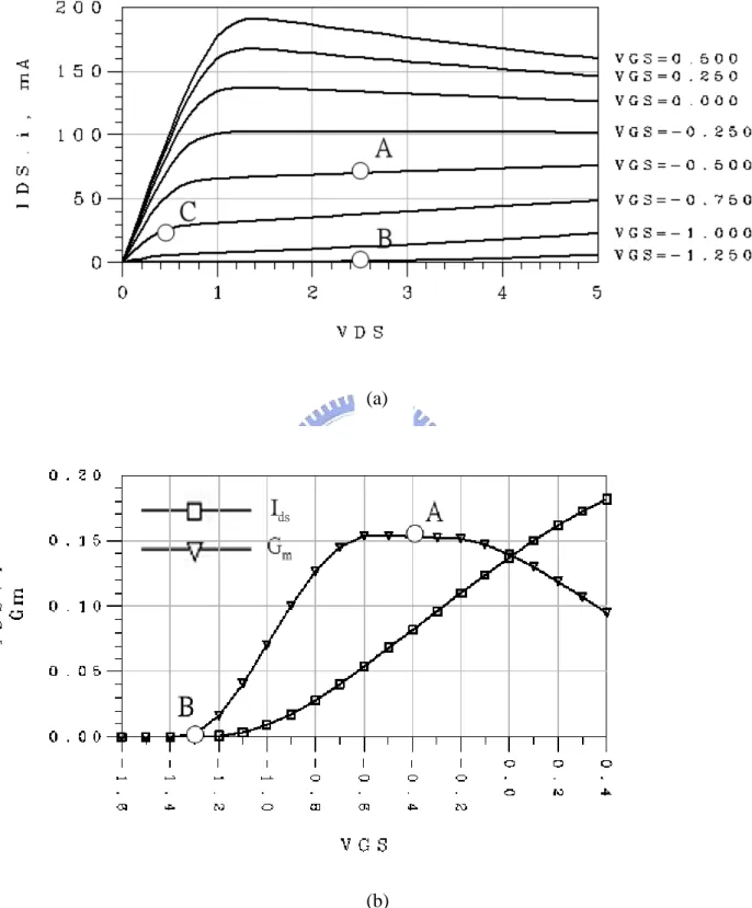
(16) structure, which is implemented by a highly doped active layer below the cathode. Active FETs. FETs are widely used in MMIC frequency multipliers, as. many monolithic foundry processes are based on the MESFET/HEMT structure. Consequently, FET frequency multipliers can be fabricated on the same chip with other FET-based circuits, such as amplifiers, oscillators, mixers and switches, to form integrated subsystems. In the large-signal modeling [3] shown in Fig. 2.2, the following six elements were assumed to be nonlinear: Rfs, Rfd, Cgs, Cgd, Gm and Gds. However, the values of Rfs and Rfd remain very large and do not contribute to the generation of higher harmonics when the input power level is not large enough to cause the gate of the Schottky junction to conduct in the forward direction. Furthermore, active FET frequency multipliers offer the potential to achieve conversion gain. Generally, they also require less input power, have higher isolation and give comparable noise performance to diode frequency multipliers.. 2.3 Biasing Points Considerations In a frequency multiplier design with passive diodes, the biasing point chosen from 0V to several hundred millivolts is generally acknowledged. It can generate higher harmonics caused by the current clipping of the diodes. By contrast, the biasing point selection, in a frequency multiplier design with active FETs, is more complicated. Among the four major nonlinearities considered in Section 2.2, the transconductance (Gm) and the output conductance (Gds) are the major elements which cause the drain current clipping and generate higher harmonics. The capacitances (Cgs and Cgd) can be considered as parasitic elements which degrade the device gain and isolation at high frequencies. Following the quasi-static approximation of [4], the current at the drain port can be expressed as. 4.
(17) Ids (vgs, vds ) = ∫ gm(v, vds )dv + ∫ gds (vT , v)dv vgs. vds. vT. 0. ,. (2.1). where vT is a gate bias value determined for best convergence from large to small signal S-parameter under small signal excitation. From (2.1), it can be inferred that there are two possible ways to generate higher harmonics: one usage is the nonlinearity of Gm and the other is that of Gds, Fig. 2.3(a) shows the behavior of Ids versus Vgs and Vds, and Fig. 2.3(b) indicates Ids, Gm versus Vgs characteristics of the FETs. Each biasing point is further discussed in the following.. 2.3.1 Class A For a class A amplifier operation [5], the quiescent gate voltage must be selected so that the drain current is set to Id0 = IDSS/2 and the drain voltage is set to Vd0 = (BVds-Vk)/2, which corresponds to a biasing point of point A in Fig. 2.3(a). The resultant maximum Gm is shown in Fig. 2.3(b). Small-signal class A operation is linear as illustrated in Fig. 2.4(a), while large-signal class A operation introduces some nonlinearities in the output signal as illustrated in Fig. 2.4(b). As depicted in Fig. 2.4(b), the nonlinear trapezoidal wave function x(t) can be expressed as 0 A c (t − ) T 0 −c 2 x(t ) = 2 A − A (t − T 0 + c ) T0 −c 2 2. c c and T 0 − ≤ t ≤ T 0 2 2 c T0 c ≤t ≤ − 2 2 2. 0≤t ≤. T0 c T0 c − ≤t ≤ + 2 2 2 2 T0 c c + ≤ t ≤T0− 2 2 2. (2.2). x(t ) = x(t + T 0) .. According to the Fourier series expansion [6], the Fourier coefficients Xn of the trapezoidal wave function x(t) can be expressed as. 5.
(18) 1 2 ncπ ) Xn = 2 cos( 0 T − n 2π 2 (1 − 2c ) T0. n=0 n = ±1,±3,±5.... ,. (2.3). the trapezoidal wave is composed of odd harmonic frequencies exclusively. Hence it appears that, in large-signal class A operation the output signal contains only odd harmonics of the fundamental signal. Consequently, the class A biasing condition is the favored choice when designing a tripler and other odd order multipliers.. 2.3.2 Class B For a class B amplifier operation [5], the bias is arranged to shut off the output device half of every cycle. In other words, the quiescent gate voltage must be set to Vg0 = Vp, and the drain voltage is set to Vd0 = (BVds-Vk)/2, which the biasing point is the same as point B, as shown in Fig. 2.3(a), near the pinch-off voltage as shown in Fig. 2.3(b). As illustrated in Fig. 2.5, when a sinusoidal signal is injected into a class B amplifier, the output signal will be half rectified, which is caused by the drain current clipping. As depicted in Fig. 2.5, the half-rectified sinusoidal wave function x(t) can be expressed as A sin ω 0t x (t ) = 0 . 0≤t ≤. T0 2. (2.4). T0 ≤ t ≤T0 2. x(t ) = x(t + T 0) .. According to the Fourier series expansion, the Fourier coefficients Xn of the half-rectified sinusoidal wave function x(t) can be expressed as. 6.
(19) A π (1 − n 2 ) 0 Xn = jA − 4 jA 4. n = 0 , ± 2 , ± 4 ... n = ± 3, ± 5 .... ,. (2.5). n =1 n = −1. except for the fundamental, the half-rectified sinusoidal wave is composed of even harmonic frequencies exclusively. Hence it appears that, in class B operation the output signal contains only even harmonics of the fundamental signal. Therefore, the class B biasing condition is the favorite choice when designing a doubler, quadrupler or other even order multipliers. The operation of a class B amplifier has a smaller time-averaged transconductance value than a class A amplifier. The pinch-off point B, however, has a lower Cgs value, smaller power consumption and is free of forward conduction current at the gate. Point B is preferable to A for high frequency operation due to the lower leakage current through Cgs; the conductance associated with Cgs becomes more significant at high frequencies and the leakage currents through the capacitance degrade the device gain and conversion gain.. 2.3.3 Resistive Concept Another possible biasing point corresponds to point C as indicated in Fig. 2.3(a). Here, the variation of Gds is the major factor to generate higher harmonics of the drain current. The channel of a FET, at low drain voltage, is a very linear resistor. It becomes significantly nonlinear only when the drain voltage becomes great enough to accelerate the electrons to their saturated drift velocity. In most FETs, this occurs at a few tenths of a volt to one volt, depending on the gate voltage. Therefore, at normal small-signal voltage of a few millivolts, the FET’s resistive channel Gds is 7.
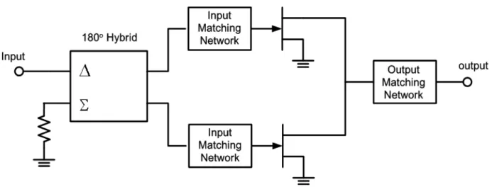
(20) very linear. The resistance of this linear channel can be varied by applying a large signal to the gate. The large signal changes the depth of the depletion region under the gate and consequently the resistance of the entire channel. When the gate voltage drops below Vp, the FET’s cutoff voltage, the resistance is virtually infinite; when the gate voltage reaches its maximum value, the channel resistance is very low, usually a few ohms. The range of resistances is entirely adequate to achieve good performance of producing higher harmonics, in which the concept is similar to the resistive mixer design theory [7]. However, the efficiency of generating higher harmonics is better with Gm than Gds.. 2.4 Frequency Multiplier Design 2.4.1 Architectures of Frequency Multipliers In general, there are two different methods to design a frequency multiplier [8]. One is single-ended and the other is balanced. Single-ended. “Single-ended” means the usage of a single nonlinear device.. Fig. 2.6 indicates the circuit of a single-ended FET frequency multiplier. This FET can generate higher harmonics to achieve a better multiplication with an appropriate bias. Balanced. Fig. 2.7 illustrates the circuit of a balanced FET frequency. multiplier. Like the single-ended configuration, it also needs an applicable bias. Moreover, the balanced configuration can be used to reduce the unwanted o. fundamental frequency, in which the cancellation is caused by the 180 out-of-phase. The balanced configuration has several advantages over the single-ended circuit. One is the nature of the phase cancellation for the fundamental frequency. The second advantage is that, like other balanced circuits, the FET balanced 8.
(21) frequency multiplier has greater bandwidth and 3 dB output power than the single-ended circuit. The third is that it is often easier to realize the load impedance of a balanced frequency multiplier than that of a single-ended circuit. Nevertheless, there are many drawbacks of the balanced configuration. The unit uses two FETs, consumes more DC power, and occupies larger chip area than that of the single-ended circuit. The usage of the coupler and combiner circuits, in a balanced configuration, is the other major die area consumption.. 2.4.2 Input and Output Matching Network Configurations The device-circuit interaction not only at the fundamental frequency, but also at the harmonic frequencies, is very crucial to the multiplication process. Although in the case of a frequency doubler it is mainly the fundamental frequency and its second harmonic to be concerned with, this still leaves transistor input and output impedance matching conditions at both these frequencies to be accounted for as potentially influential design considerations, in addition to the general dependence on the drive levels [9], [10]. The basic FET frequency doubler configuration is shown in Fig. 2.8, exhibiting a FET in common source configuration flanked by matching networks which match the gate-source port of the device to the generator at the fundamental frequency and the device drain-source port to the external load at the second harmonic frequency. A more rigorous design must be capable of undesired harmonics suppression such as a quarter-wavelength short-circuited stub, with respect to fundamental frequency, at the gate-source port of the device to suppress second harmonic frequency leakage and a quarter-wavelength open-circuited stub, with respect to fundamental frequency, at the drain-source port of the device to suppress fundamental frequency leakage. In addition, biasing circuits for the gate-source and drain-source port are also involved. 9.
(22) (a). (b). Fig. 2.1 The Schottky barrier diode (SBD) with (a) general structure, (b) its equivalent circuit.. Fig. 2.2 The large-signal model of a FET. 10.
(23) (a). (b) Fig. 2.3 DC characteristics of the FET. (a) Ids versus Vgs and Vds, (b) Ids and Gm versus Vgs at Vds = 1.5 V.. 11.
(24) (a). (b) Fig. 2.4 Class A operation with (a) small-signal, (b) large-signal.. 12.
(25) Fig. 2.5 Class B operation.. Fig. 2.6 The single-ended configuration of a frequency multiplier.. 13.
(26) Fig. 2.7 The balanced configuration of a frequency multiplier.. Fig. 2.8 The basic configuration of a frequency doubler.. 14.
(27) Chapter 3 FREQUENCY MULTIPLIER USING INGAAS PHEMT 3.1 Overview Based on the analysis and design methodology described in Chapter 2, this chapter demonstrates a 35-to-70 GHz millimeter-wave frequency doubler using InGaAs pHEMT. The fabrication, design and simulations of the circuit will be presented in the following. The measurement considerations are also specified in detail and the measured results are depicted in the last section.. 3.2 MMIC Foundry Description The pHEMT device used in this design is fabricated by WIN Semiconductor Corp. with a standard 0.15-um high-power InGaAs pHEMT MMIC process. The process employs a hybrid lithographic approach using direct-write electron beam (E-beam) lithography for sub-micron T-gate definition and optical lithography for the other process steps. The pHEMT devices are grown using molecular beam epitaxy (MBE) on 6-inch semi-insulating (SI) GaAs substrates. The pHEMT device has a typical unit current gain cutoff frequency (ft) of 85 GHz and maximum oscillation frequency (fmax) of 200 GHz. The peak DC transconductance (Gm) at -0.45 V gate-source voltage is 495 mS/mm. The gate-drain breakdown voltage is 10 V, and the maximum drain current at 0.5 V gate-source voltage is 650 mA/mm. Other passive components include thin-film resistor (TFR), mesa-resistor (epitaxial layer), metal-insulator-metal (MIM) capacitors, spiral inductors, and air-bridges. The wafer is thinned to 100 um for the backside metal plating and reactive ion etching (RIE) via-holes are used for DC grounding. 15.
(28) 3.3 35-to-70 GHz Frequency Doubler using InGaAs pHEMT 3.3.1 Circuit Design Fig. 3.1 indicates the schematic diagram of the 35-to-70 GHz frequency doubler. In order to minimize the chip area and the DC power consumption, the single-ended frequency doubler configuration was adopted. This circuit was designed using microstrip transmission lines. The nonlinear device is an InGaAs pHEMT with 4 x 75 um gate width. An effective way to employ an InGaAs pHEMT as a frequency doubler is to use it as a half-wave rectifier which is described in Section 2.3.2. Consequently, the operating condition near the pinch-off region (Vgs = -0.95V, Vds = 1.45V) with 14.5 mW power consumption was chosen to generate higher even harmonic power level. One quarter-wavelength open-circuited radial stub functions as a 35 GHz bandstop filter to reject the fundamental frequency at drain. The radial stub has wider bandwidth and higher rejection of more than 20 dB. The gate bias is injected through a thin-film resistor connected to a decoupling MIM capacitor and a high impedance transmission line. This resistor stabilizes the InGaAs pHEMT at low frequencies. The combination of the resistor, capacitor and high impedance transmission line impedance is equivalent to a quarter-wavelength to yield the open condition at the input line. The decoupling circuit for the drain bias is realized via the similar method. The input port, with a DC blocking MIM capacitor, was matched to receive maximum power at the fundamental frequency of 35 GHz. The output port, with a DC blocking coupled-line, was matched to deliver maximum power at second harmonic frequency of 70 GHz. The matching networks at the input and output of the circuit are achieved using 50O open-circuited stubs. A layout of the 35-to-70 GHz frequency doubler with chip size of 2 x 1 mm2 is accomplished by 16.
(29) the Cadence tools and is depicted in Fig. 3.2.. 3.3.2 Simulated Results The nonlinear InGaAs pHEMT model used in the simulation is a HP EEsof scalable nonlinear HEMT model (EE_HEMT model) provided by the foundry. The 35-to-70 GHz frequency doubler performance is simulated via the harmonic balance technique implemented in the commercial computer-aided design (CAD) software Agilent Advanced Design System (ADS). All the matching, biasing and other passive circuits are simulated through an electromagnetic (EM) full-wave simulator SONNET. Conversion and rejection performances are the important specifications for a frequency doubler design. The definition of conversion gain is that the second harmonic output power minus the fundamental input power. The fundamental rejection is defined as the fundamental output power minus the fundamental input power, and the third harmonic rejection is defined as the third harmonic output power minus the fundamental input power. They are usually expressed in decibels. The simulated conversion gain, fundamental rejection, third harmonic rejection and output power versus input power from -10 to 15 dBm at input frequency of 35 GHz are plotted in Fig. 3.3 and Fig. 3.4. It is observed that, for an input power level at 3 dBm, the conversion performance achieves a maximum conversion gain of -6.5 dB. The saturated output power at 70 GHz is almost 0 dBm for 15 dBm input power. Fig. 3.5(a) and Fig. 3.5(b) also indicate the simulated conversion gain, fundamental rejection and third harmonic rejection as a function of input frequency from 32 to 38 GHz with an input power level of 1 and 6 dBm. It has around 1 GHz bandwidth centered at 35 GHz for a flat conversion gain. The simulated small-signal S-parameters from 20 to 50 GHz and 60 to 80 GHz, illustrated in Fig. 3.6(a) and Fig 17.
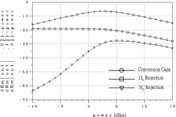
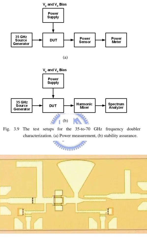
(30) 3.6(b), give some assurances that the input and output ports are matched to nearly 50O standard. Fig. 3.7 shows the simulated large-signal S-parameters from 30 to 40 GHz with input frequency of 35 GHz and output frequency of 70 GHz for 1 dBm input power.. 3.3.3 Measurement Considerations In the millimeter-wave frequency range, two significant concerns of the 35-to-70 GHz frequency doubler should be taken into account. One is the power measurement and the other is the stability assurance. Power Measurement. To acquire the absolutely accurate power level at 70. GHz, a V-band waveguide power sensor is required. The power sensor calculates each power value of the in-band frequencies resulting in a total power level. Accordingly, only the 70 GHz signal can exist to guarantee an accurate measurement. Indeed, a power meter, with calibrated calibration factors (CF) at each frequency, must be connected to the power sensor to depict the value of the measured power level. Stability Assurance. The stability assurance is the key point to certify the. accuracy for the power measurement. A spectrum analyzer (SA) can be used to verify whether the undesired oscillation occurs or not. Nevertheless, the commercially available SAs are not capable of directly measurement up to the V-band, W-band or higher frequencies. An external harmonic mixer should be applied with the SA to perform the down-conversion of the V-band, W-band or higher frequencies down to the lower frequency band. Therefore, we can still validate the frequency spectrum of the V-band, W-band or higher frequencies via the commercially available SAs and external harmonic mixers with the calibrated conversion loss (CL) and reference level offset. The harmonic mixing causes many 18.
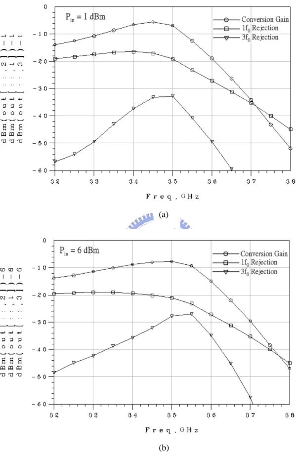
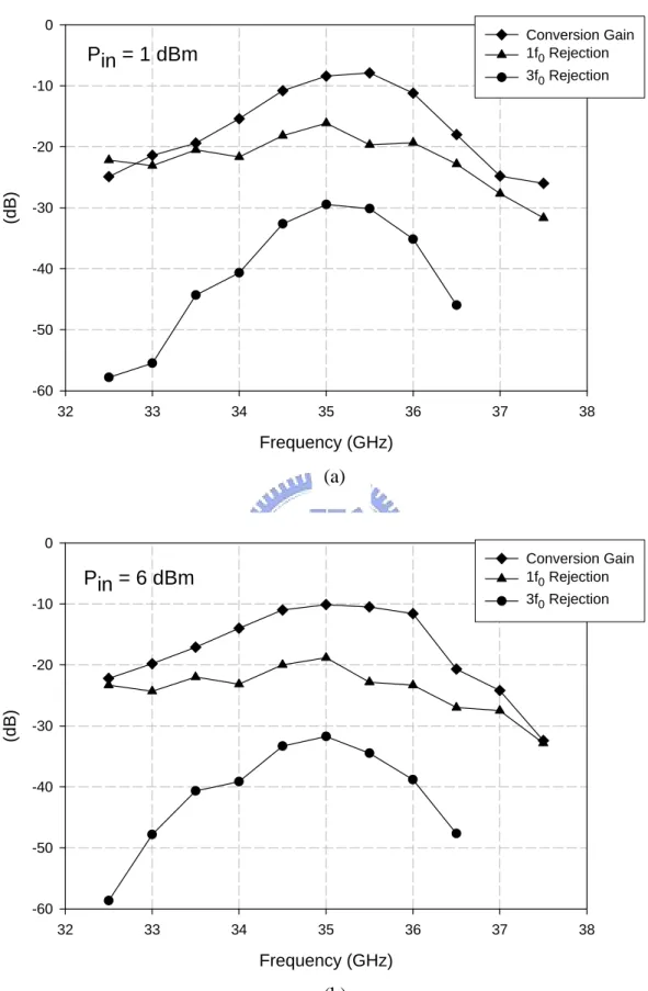
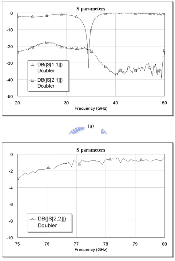
(31) mixer products (mfRF + nfLO) at the intermediate frequency (IF) output. As a result, within a single harmonic band, a single input signal can produce multiple responses on the analyzer display as illustrated in Fig. 3.8 (in this case, the 76 GHz signal is valid), only one of which is valid. These responses come in pairs, where members of the valid response pair are separated almost to 2fIF and either the right-most (for negative harmonics) or left-most (for positive harmonics) member of the pair is the correct response. To identify the actual signals from the undesired images and spurs, a frequency-shift method can be applied. The altered quantity of the actual signals must consist with the shift of the radio frequency (RF) or local oscillator (LO) when either the RF or LO frequency is shifted. Otherwise, the remains are the undesired images and spurs. For some newer types of the SAs, identification of valid responses is achieved by simply turning on the signal-identification (SIG ID) feature.. 3.3.4 Measured Results The 35-to-70 GHz frequency doubler was measured via on-wafer probing. Fig. 3.9(a) and Fig. 3.9(b) illustrate the test setups used for the circuit characterization. The former is established for power measurement and the latter verifies the stability assurance. A microphotograph of the 35-to-70 GHz frequency doubler is shown in Fig. 3.10. The measured conversion gain, fundamental rejection, third harmonic rejection and output power versus input power from -10 to 15 dBm at input frequency of 35 GHz are plotted in Fig. 3.11 and Fig. 3.12. It is observed that, for an input power level at 1 dBm, the conversion performance achieves a maximum conversion gain of -8.4 dB. The saturated output power at 70 GHz is -2.6 dBm for 15 dBm input power. Fig. 3.13(a) and Fig. 3.13(b) also indicate the measured conversion gain, fundamental rejection and third harmonic rejection as a function of input frequency 19.
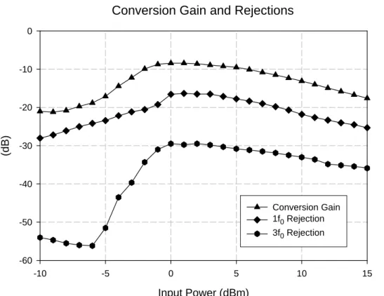
(32) from 32.5 to 37.5 GHz with an input power level of 1 and 6 dBm. It has almost 1 GHz bandwidth centered at 35 GHz for a flat conversion gain. The measured small-signal S-parameters from 20 to 50 GHz and 75 to 80 GHz, illustrated in Fig. 3.14(a) and Fig. 3.14(b), give some agreements with that the input and output ports are matched to nearly 50O standard. As discussed in Section 3.3.3, stability assurance is an important factor to guarantee the accuracy of the power measurement. Fig. 3.15 and Fig. 3.16 depict the frequency spectrum from 58 to 75 GHz and 75 to 110 GHz. Only the 70 and 105 GHz signals are valid and the others are images and spurs. It can be confirmed by the RF-shift technique. When the fundamental 35 GHz input signal was shifted by 1 MHz, not only the second harmonic 70 GHz output signal was shifted by 2 MHz as illustrated in Fig. 3.17(a), but also the third harmonic 105 GHz output signal was shifted by 3 MHz as illustrated in Fig. 3.17(b). If an oscillating signal appears within 58 to 110 GHz, the shift must be zero caused by the unchanged LO frequency. For example, the 61.2 and 78.09 GHz signals are shifted by 1.75 and 2.258 MHz as indicated in Fig. 3.17(c) and Fig 3.17(d). Consequently, they are not actual signals. Similarly, the others which are verified by RF-shift, are also images and spurs except for the 70 and 105 GHz signals. Fig. 3.18(a) indicates none of the low frequency oscillations from DC to 40 GHz. The 35 GHz signal is the leakage from the input signal. A more rigorous inspection from DC to 1 GHz frequency spectrum is shown in Fig 3.18(b). Therefore, we can confirm that this 35-to-70 GHz frequency doubler is stable for the above frequency bands. Furthermore, if a low frequency oscillation caused by the impurity of power supply or other defects occurs, an out-of-chip capacitor can be added to the drain or gate port to eliminate the oscillation.. 20.
(33) Fig. 3.1 The schematic diagram of the 35-to-70 GHz frequency doubler.. Fig. 3.2 Layout of the 35-to-70 GHz frequency doubler.. 21.
(34) Fig. 3.3 The simulated conversion gain, 1f0 and 3f0 rejection versus input power of the 35-to-70 GHz frequency doubler.. Fig. 3.4 The simulated output power versus input power of the 35-to-70 GHz frequency doubler. 22.
(35) (a). (b) Fig. 3.5 The simulated conversion gain, 1f0 and 3f0 rejection versus frequency of the 35-to-70 GHz frequency doubler at (a) Pin = 1dBm, (b) Pin = 6dBm.. 23.
(36) (a). (b) Fig. 3.6 The simulated small-signal S-parameters of the 35-to-70 GHz frequency doubler. (a) From 20 to 50 GHz for S11 and S21, (b) from 60 to 80 GHz for S22.. 24.
(37) Fig. 3.7 The simulated large-signal S-parameters of the 35-to-70 GHz frequency doubler from 30 to 40 GHz for S11, S21 and S22.. Fig. 3.8 Signal responses produced by a 76 GHz signal in W-band.. 25.
(38) (a). (b) Fig. 3.9 The test setups for the 35-to-70 GHz frequency doubler characterization. (a) Power measurement, (b) stability assurance.. Fig. 3.10 The microphotograph of the 35-to-70 GHz frequency doubler.. 26.
(39) Conversion Gain and Rejections 0. -10. (dB). -20. -30. -40 Conversion Gain 1f0 Rejection. -50. 3f0 Rejection -60 -10. -5. 0. 5. 10. 15. Input Power (dBm). Fig. 3.11 The measured conversion gain, 1f0 and 3f0 rejection versus input power of the 35-to-70 GHz frequency doubler.. Pout vs Pin 0. -10. (dBm). -20. -30. -40 Pout(2f0) vs Pin Pout(1f0) vs Pin. -50. Pout(3f0) vs Pin -60. -70 -10. -5. 0. 5. 10. 15. Input Power (dBm). Fig. 3.12 The measured output power versus input power of the 35-to-70 GHz frequency doubler. 27.
(40) 0. Conversion Gain 1f0 Rejection. Pin = 1 dBm. 3f0 Rejection. -10. (dB). -20. -30. -40. -50. -60 32. 33. 34. 35. 36. 37. 38. Frequency (GHz). (a). 0 Conversion Gain 1f0 Rejection. Pin = 6 dBm. 3f0 Rejection. -10. (dB). -20. -30. -40. -50. -60 32. 33. 34. 35. 36. 37. 38. Frequency (GHz). (b) Fig. 3.13 The simulated conversion gain, 1f0 and 3f0 rejection versus frequency of the 35-to-70 GHz frequency doubler at (a) Pin = 1dBm, (b) Pin = 6dBm.. 28.
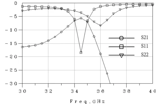
(41) (a). (b) Fig. 3.14 The measured small-signal S-parameters of the 35-to-70 GHz frequency doubler. (a) From 20 to 50 GHz for S11 and S21, (b) from 75 to 80 GHz for S22.. 29.
(42) Fig. 3.15 Frequency spectrum from 58 to 75 GHz produced by a 70 GHz signal.. Fig. 3.16 Frequency spectrum from 75 to 110 GHz produced by a 105 GHz signal.. 30.
(43) (a). (b). (c). (d). Fig. 3.17 (a) A 70 GHz real signal, (b) a 105 GHz real signal, (c) a 61.2 GHz spurious signal, (d) a 78.09 GHz spurious signal.. (a). (b). Fig. 3.18 Frequency spectrum produced by a 35 GHz leakage signal, (a) from 0 to 40 GHz, (b) from 0 to 1 GHz. 31.
(44) Chapter 4 DESIGN METHODOLOGY OF BROADBAND SWITCHES 4.1 Overview A switch can be applied to perform the multiple accesses, which is widely used and considered as a major choice in communications. It also reduces the duplicate of the circuits with identical functions. In the low frequency below several GHz, the design of switches merely concerns the parasitics and transmission-line effects. On the contrary, these effects appear significantly in the millimeter-wave frequency range and must be taken into account in the switch design. This chapter has a full discussion on the design methodology of broadband switches and presents the Fisher’s equivalence [11] in order to broaden the bandwidth of switches.. 4.2 Switching Devices Two types of devices used commonly in the control circuits are PIN diodes and FETs. Before looking at the circuit design methods, we briefly review the significant properties of these devices. PIN Diodes. A PIN diode is a pn junction device that has a very minimally. doped or intrinsic region located between the p-type and n-type contact regions as illustrated in Fig. 4.1(a). The addition of the intrinsic or i-region results in characteristics that is very superior for certain device applications. In reverse bias the intrinsic region results in very high values for the diode breakdown voltage, whereas the device capacitance is reduced by the increased separation between the p- and n-region. In forward bias the conductivity of the intrinsic region is controlled or modulated by the injection of charge from the end regions. A practical PIN diode 32.
(45) consists of a lightly doped p- or n-region between the highly doped p-type and n-type contact regions, as shown in Fig. 4.1(b) and Fig. 4.1(c). To identify very lightly doped p and n material, the Greek letters are used; consequently, lightly doped p material is called p-type and lightly doped n material is called ?-type. The diode is a bias-current-controlled resistor with preferable linearity and low distortion. PIN diodes can provide faster switching speed and can handle medium to large RF power levels. They also make excellent RF switches, phase shifters and limiters. Sometimes the Schottky barrier diode (SBD) is applied for faster switching speed. FETs. In recent years PIN diode switches have been increasingly. replaced by FETs based monolithic switches, especially for low to medium power applications. The FET switches are three-terminal devices, in which the gate bias voltage Vg controls the states of the switch. The FET acts as a voltage-controlled resistor, in which the gate bias controls the drain-to-source resistance in the channel. The intrinsic gate-to-source and gate-to-drain capacitances and device parasitics limit the performance of the FET switches at higher frequencies. In switching applications, a low-impedance (nearly short) state is obtained by making the gate voltage equal to zero. When the negative gate-source bias is larger than the pinch-off voltage in magnitude, the FET is in a high-impedance (nearly open) state. Fig. 4.2 shows these two linear operational regions of the FET graphically [12]. Fig. 4.3 indicates the configuration of a switching FET [13]. A low-impedance state can be adequately modeled by a DC “on” resistance (Ron) which is series connection to a parasitic inductor (Lon) between the source and the drain as depicted in Fig. 4.4(a). Additional parasitic elements exist, but have no influential RF effects, particularly if the gate bias circuitry is isolated with a large value resistor (Riso), as is indicated in Fig. 4.3. A complete equivalent circuit in a high-impedance state is illustrated in Fig. 4.4(b). This equivalent circuit is based on the device geometry and has been 33.
(46) described previously in [12], [14]. The off-state drain-to-source leakage resistance (Rds) is generally large enough to be neglected in circuit modeling. The drain and the source are directly capacitive-coupled (Cds) and also through the gate (Cgs and Cgd). All of these capacitances have series parasitic resistive elements (Rgs and Rgd for Cgs and Cgd; Rs and Rd for Cds). A simplified FET model can be used without sacrificing accuracy as shown in Fig. 4.5(a) and Fig. 4.5(b). The parasitic inductor was neglected for the on-state equivalent circuit. The off-state equivalent circuit has been reduced to a simple series resistor (Roff) and capacitor (Coff). For the simplification, it is assumed that the magnitudes of the reactances of the various capacitances are much greater than the various parasitic resistances. This assumption yields the following relationships: Roff ≈. 1. Coff. Rgs + Rgd Rs + Rd + Cds (Cgs + Cgd ) 2 [1 + ]2 [1 + ] (Cgs + Cgd ) Cds. ≈. 1 (Cgs + Cgd ) 1 Cds + . Cds (Cgs + Cgd ) 2 2 [1 + ] [1 + ] Cds (Cgs + Cgd ). (4.1). (4.2). Note that these relationships for Roff and Coff are frequency independent. The additional terms that have been ignored are frequency dependent. It is important to note that virtually no DC power is required by the FET switches in either state. The other advantage of FET switches is that additional biasing circuits are unnecessary because of the natural DC isolation between gate and drain (or source). The negligible DC power consumption and DC biasing isolation of the FET switches are superior to the PIN diode switches.. 4.3 Broadband Switch Design 4.3.1 Basic Switch Configurations 34.
(47) There are two basic configurations [15] that may be used for a simple switch designed to control the flow of millimeter-wave signals along a transmission line. One is series-type switch and the other is shunt-type switch. The third configuration that consists of the combination of the series-type and shunt-type switches is called series-shunt switch. Before we go into the details, two essential parameters of switches must be specified. Insertion loss (IL) is defined as the ratio of the power delivered to the load in the on-state of the ideal switch to the actual power delivered by the practical switch. It is usually expressed in decibels. Isolation is a measure of the performance for the switch when it is in the off-state. Isolation (ISO) is defined as the ratio of the power delivered to the load for an ideal switch in the on-state to the actual power delivered to the load when the switch is in the off-state. Series-type Switches. Fig. 4.6(a) illustrates the equivalent circuit of a. series-type switch. The low-impedance state of the FET allows the signal to propagate, while in the high-impedance state, the incident power on the switch is mostly reflected back. Accordingly, the low- and high-impedance states of the FET are called on-state and off-state for a series-type switch. The insertion loss may be calculated by considering the equivalent circuit depicted in Fig 4.6(b). If VL denotes the actual voltage across the load in the ideal switch, the insertion loss may be written as 2. 2. VL Rlow 1 Rlow 1 Xlow IL = = 1+ + + VLD Z0 4 Z0 4 Z0 . 2. ,. (4.3). where Zlow = Rlow + jXlow is the impedance of the switching device in the low-impedance state. Similarly, the isolation is given as. 35.
(48) 2. ISO =. 2. VL Rhigh 1 Rhigh 1 Xhigh = 1+ + + VLD Z0 4 Z0 4 Z0 . 2. ,. (4.4). where Zhigh = Rhigh + jXhigh is the impedance of the switching device in the high-impedance state. Shunt-type Switches. Fig. 4.7(a) illustrates the equivalent circuit of a. shunt-type switch. The shunt-type switch is complement to the series-type switch. The low-impedance state of the FET almost reflects the incident power back and the high-impedance state permits the signal to propagate. Therefore, the low- and high-impedance states of the FET are called off-state and on-state for a shunt-type switch. The insertion loss may also be calculated by considering the equivalent circuit depicted in Fig 4.7(b). If VL denotes the actual voltage across the load in the ideal switch, the insertion loss may be written as 2. 2. VL Ghigh 1 Ghigh 1 Bhigh IL = = 1+ + + VLD Y0 4 Y0 4 Y0 . 2. ,. (4.5). where Yhigh = Ghigh + jBhigh is the admittance of the switching device in the high-impedance state. Furthermore, the isolation is given as 2. ISO =. 2. VL Glow 1 Ylow 1 Blow = 1+ + + VLD Y0 4 Y0 4 Y0 . 2. ,. (4.6). where Ylow = Glow + jBlow is the admittance of the switching device in the low-impedance state. Series-Shunt Switches. The simplest series-shunt switching configuration is. indicated in Fig. 4.8(a). This switching circuit may be analyzed in terms of the equivalent circuit as shown in Fig. 4.8(b). For the on-state, the device impedance Zse is denoted by the low impedance Zlow, and the device impedance Zsh is denoted by 36.
(49) the high impedance Zhigh. From the simple circuit analysis, the insertion loss may be written as 1 ( Z 0 + Zhigh)( Z 0 + Zlow) IL = + 2 2 Z 0 Zhigh. 2. .. (4.7). .. (4.8). Similarly, the isolation is written as 1 ( Z 0 + Zlow)( Z 0 + Zhigh ) ISO = + 2 2 Z 0 Zlow. 2. It may be noted that if the non-identical devices are used in the series and the shunt locations, values of Zhigh and Zlow in (4.7) could be different from those in (4.8). In general, the isolation obtained by using a series-shunt configuration is much better (more than twice in decibels) than that for either the series-type or shunt-type switch. The insertion loss for the series-shunt configuration is worse than that for a shunt-type switch but better than that for a series-type switch.. 4.3.2 Single-Pole Single-Throw Switch A single-pole single-throw (SPST) switch is used to control the flow of signals along a transmission line. As mentioned above, three basic configurations can be adopted to design the SPST switch. In the millimeter-wave frequency range, the device parasitics introduce more significantly unfavorable effects either on insertion or isolation performance. Some well-known compensated techniques, like capacitive [16] or impedance-transformation methods [17], can be utilized to minimize the non-ideal open or non-ideal short effects. Even a traveling-wave concept was applied in SPST switch design [18]. In 1965, R. E. Fisher [11] has suggested that the diode capacitance and its parallel resonating stub tuner could be analyzed approximately as a simple stub. J. F. 37.
(50) White [19] demonstrates the feasibility of Fisher’s equivalence for low frequencies from 1 to 2 GHz in 1968. In this thesis, Fisher’s equivalence is also adopted except that the switching devices are replaced by FETs and the frequencies are extended to the millimeter-wave frequency range. Fig. 4.9 illustrates the circuit model used for Fisher’s equivalent circuit. The following equation gives the relationship between YE, YT ,θ T and the diode capacitance C.. −1 ω 0C ω 0C 2 2 YE = ω 0C + YT cot 1 + π YT YT . (4.9). Fig. 4.10 plots YT and θT versus ω0C/YE. For a more accurate estimation, some corresponding variable values for the common steps in the evaluation of ω0C/YE are given in Table 4.1. For small normalized susceptance, ω0C/YE, the required tuning stub is nearly a quarter wavelength long and its normalized admittance, YT/YE, is nearly unity. The largest allowable value forω0C/YE is p/4. As can be seen from the curves, θT and YT/YE are both equal to zero at this value. Furthermore, a maximally flat filter, consisting of the quarter-wavelength short-circuited stubs with quarter-wavelength spacing, has been summarized in tabular form by W. W. Mumford [20]. The form of the filter is shown in Fig. 4.11 and Mumford’s values for filters with three, four and five elements are tabulated in Table 4.2. The filters are symmetrical and consequently only the normalized admittances for the first stub to the center are listed. For a broadband SPST switch design, the parasitics of FETs in the low-impedance state are usually unconcerned and can simply be ignored. In the high-impedance state, the parasitic capacitances of FETs have more significant effects, but they can also be incorporated into the equivalent quarter-wavelength 38.
(51) short-circuited stubs, as illustrated in Fig. 4.12, to broaden the bandwidth of SPST switches. To be more specific, a wide bandwidth of the maximally flat filter can be created via the design tables or calculations by hands first. The parasitic capacitances of FETs can be equivalent to the capacitors modeled in the Fisher’s equivalence and be transformed to the quarter-wavelength short-circuited stubs used in the previously wideband filter. Therefore, an arbitrarily broadband SPST switch can be formed with an appropriate design through the technique of capacitances absorption.. 4.3.3 Single-Pole Double-Throw Switch Fig. 4.13(a) and Fig. 4.13(b) show the series-type and shunt-type circuits for a single-pole double-throw (SPDT) switch; the switch demands at least two switching devices. In operation, one FET is biased in the low-impedance state, while the other FET is biased in the high-impedances state. The input signal is switched from one output to the other by reversing the FET states. The bandwidth of the SPDT switch in shunt configuration is restricted because of the quarter-wavelength transmission line, which is required between the transmission line junction and the locations of the two switching devices. Fisher also suggested that a SPDT shunt diode tee switch can be realized using the stub filter approach; such a method is depicted in Fig. 4.14(a). The diodes are located a quarter-wavelength apart from the input in each of two output arms. The off-arm has a nearly short circuit produced by the forward biased diode, which results in a quarter-wavelength short-circuited stub shunted with the transmission path to the on-arm. As shown in Fig. 4.14(b), this stub must have the characteristic admittance, Y0, of the through line since it represents a transmission path when it becomes an on-arm. 39.
(52) To be more definite, the parasitic capacitances of FETs, in the high-impedance state, can also be incorporated into the equivalent quarter-wavelength short-circuited stubs used in the previously wideband filter as described in Section 4.3.2. This design is distinct from the conventional ones, in which the bandwidth is restricted because of the quarter-wavelength transmission line which is required between the transmission line junction and the locations of the two switching devices. The extra quarter-wavelength transmission line can be incorporated into the transmission path for the on-arm as indicated in Fig 4.14(b). Consequently, an arbitrarily broadband SPDT switch can be formed with an appropriate design through the technique of capacitances absorption.. 4.3.4 Single-Pole m-Throw Switch The single-pole m-throw (SPmT) switch has a single input, a single output on-arm and (m-1) output off-arms. We proposed that a SPmT shunt-type switch can also be realized using the stub filter approach. The FETs are located a quarter-wavelength apart from the input in each of the m output arms. The (m-1) off-arms have a nearly short circuit produced by the low-impedance FETs, which result in an equivalent quarter-wavelength short-circuited stub with the characteristic admittance of (m-1)Y0 shunted with the transmission path to the on-arm. Each stub must have the characteristic admittance, Y0, of the through line since it represents a transmission path when it becomes an on-arm. The last of the quarter-wavelength short-circuited stubs for each paths must have the characteristic admittance of (m-1)Y0 which is corresponding to the equivalent quarter-wavelength short-circuited stub resulted from the (m-1) shunted off-arms. Therefore, the bandwidth of this proposed SPmT switch can be almost unrestricted if an appropriate design is employed. 40.
(53) (a). (b). (c). Fig. 4.1 (a) A general structure of the PIN diode, (b) ?-type, (c) p-type.. Fig. 4.2 Linear operational regions of a FET switch.. 41.
(54) Fig. 4.3 The FET in switching configuration.. (a). (b). (a). Fig. 4.4 Complete equivalent circuit for, (a) low-impedance state, (b) high-impedance state.. (b). Fig. 4.5 Simplified equivalent circuit for, (a) low-impedance state, (b) high-impedance state.. (a). (b) Fig. 4.6 Series-type switch configuration, (a) transmission line model, (b) equivalent circuit model. 42.
(55) (a). (b) Fig. 4.7 Shunt-type switch configuration, (a) transmission line model, (b) equivalent circuit model.. (a). (b) Fig. 4.8 Series-shunt switch configuration, (a) transmission line model, (b) equivalent circuit model.. 43.
(56) Fig. 4.9 Circuit model used for Fisher’s equivalent circuit.. Fig. 4.10 Summary of Fisher’s equivalence for simulating a quarter-wavelength stub with a capacitor and its parallel tuner.. ω0C / YE. YT / YE. θT (degree). 0.000. 1.000. 90.0. 0.100. 0.985. 84.2. 0.200. 0.956. 78.4. 0.300. 0.915. 71.8. 0.400. 0.850. 64.8. 0.500. 0.760. 56.7. 0.600. 0.627. 46.2. 0.700. 0.436. 31.9. 0.750. 0.300. 21.8. 0.780. 0.120. 8.75. 0.7854(π/4). 0.000. 0.00. Table 4.1 Tuned capacitor values for simulating a quarter-wavelength stub.. Fig. 4.11 Equivalent circuit for the maximally flat stub filter.. 44.
(57) Y2 / Y0. 0.100. 0.200. 0.300. 0.600. 0.500. 1.000. Y1 / Y0. Y2 / Y0. Y3 / Y0. 0.700. 1.400. 0.100. 0.366. 0.532. 1.000. 2.000. 0.200. 0.694. 0.989. 1.400. 2.800. 0.300. 1.005. 1.410. 2.000. 4.000. 0.400. 1.304. 1.808. 2.500. 5.000. 0.500. 1.596. 2.193. 3.000. 6.000. 0.700. 2.166. 2.933. 0.100. 0.292. 0.900. 2.724. 3.648. 0.200. 0.571. 1.300. 3.819. 5.038. 0.400. 1.109. 2.000. 5.702. 7.403. 0.800. 2.141. 2.800. 7.829. 10.058. 1.300. 3.395. 1.900. 4.877. 3.000. 7.568. Five Stubs. Three Stubs Four Stubs. Y1 / Y0. Table 4.2 Mumford’s design tables for the maximally flat stub filters.. Fig. 4.12 Equivalent circuit for the transmission state of the SPST switch.. 45.
(58) (a). (b) Fig. 4.13 The SPDT switch with, (a) series-type configuration, (b) shunt-type configuration.. (a). (b) Fig. 4.14 (a) SPDT switch implemented by Fisher’s equivalence, (b) the equivalent filter circuit for the transmission state. 46.
數據
+7

相關文件
定義為∣G(jω)∣降至零頻率增益(直流增益)值之 0.707 倍 時之頻率或-3dB 時頻率。.
單晶片電路接受到 A/D 轉換器的信號後,即將此數位信號由顥示器 顯示。此時單晶片 IC 並將此一 A/D 轉換器與指撥設定開關做比較,A/D 轉換器的信號高於設定值時,即由 OUT CONTROL
接收器: 目前敲擊回音法所採用的接收 器為一種寬頻的位移接收器 其與物體表
雙極性接面電晶體(bipolar junction transistor, BJT) 場效電晶體(field effect transistor, FET).
• A function is a piece of program code that accepts input arguments from the caller, and then returns output arguments to the caller.. • In MATLAB, the syntax of functions is
Sequence-to-sequence learning: both input and output are both sequences with different lengths..
This design the quadrature voltage-controlled oscillator and measure center frequency, output power, phase noise and output waveform, these four parameters. In four parameters
傳統的 RF front-end 常定義在高頻無線通訊的接收端電路,例如類比 式 AM/FM 通訊、微波通訊等。射頻(Radio frequency,
