國 立 交 通 大 學
工學院半導體材料與製程設備學程
碩士論文
動態隨機存取記憶體(DRAM)電容清洗技術之研究
The Study of Cleaning Methods for Dynamic Random
Access Memory (DRAM) Capacitor
研究生: 吳慧盈
指導教授 : 張 立 博士
動態隨機存取記憶體(DRAM)電容清洗技術之研究
The Study of Cleaning Methods for Dynamic Random
Access Memory (DRAM) Capacitor
研 究 生:吳慧盈 Student:Wei Yeeng, Ng
指導教授:張立 Advisor:Li, Chang
國 立 交 通 大 學
工學院半導體材料與製程設備學程
碩 士 論 文
A ThesisSubmitted to Degree Program of Semiconductor Material and Process Equipment College of Engineering
National Chiao Tung University in partial Fulfillment of the Requirements
for the Degree of Master of Science in
Semiconductor Material and Process Equipment
March 2011
Hsinchu, Taiwan, Republic of China
I 動態隨機存取記憶體(DRAM)電容清洗技術之研究 學生:吳慧盈 指導教授: 張立 博士 國立交通大學工學院半導體材料與製程設備學程 摘 要 堆疊式電容為動態隨機存取記憶體(DRAM)的關鍵組件。為增加電容值,目前製程 大多利用高選擇比之氫氟酸將氮化鈦(TiN)下電極周圍之介電質做濕式等向性回 蝕刻(Crown Wet Etching Back Process),以期達到雙倍表面積的覆蓋率(Surface Area Coverage)之目的。回蝕刻製程後易產生許多副產物與雜質並會重新附著於 晶圓表面,進一步影響到製程良率。研究中藉由應用材料公司(Applied Material) 所發展之缺陷量測機台做掃描式電子顯微鏡(SEM)外觀分析及 X 光能量分散光譜 (EDS)元素分析後得知副產物成分以碳(Carbon)、矽(Silicon)、鈦(Titanium) 及氧(Oxygen)為主。本研究主要目的為找出一個適合高深寬比電容結構的清洗方 式,期能去除電容製程後所產生之副產物並避免電容結構倒塌且維持電容間的電 子特性。研究方向包含選取適當機台(單片處理機台或批次噴灑式處理機台)及不 同種類 pH 值之混合酸液(EKC6800、REZI38、EKC265、ELM C30、EcoPeeler)。決 定出最適當的機台與酸液後,將進一步探討處理時間與旋轉速度對雜質及副產物 去除能力之影響。
研究結果顯示之最佳條件為兼具製程容忍度大且雜質去除率最高的條件:酸 液 EKC265 搭配批次噴灑式處理機台。含氰胺(HDA)之化學混合溶劑 EKC265,使 雜質與基板之間的界面電位(zeta potential)處於同極性而互相排斥,進而提升 雜質去除率。氰胺為強氧化還原劑,使金屬氧化物質還原成可溶於異丙酮(IPA) 之螯合物。此外選擇應用於 EKC265 處理時間則不宜過久,若處理時間太長 Titanium 將被過度回蝕刻,結構易倒塌;然則太短雜質去除率有限,多種不同 處理時間經搭配並選擇適當之旋轉速度後所得最佳化條件,可使雜質去除率達到 80%。旋轉速度低於 650rpm 以下則雜質去除率呈線性,但於 650rpm 以上去除率 則下降;主要原因為化學反應效果於 650rpm 以上被限制全由物理力量主導所致。 最後的最佳化條件經重複驗證後,被證實可用於 60nm 以下之動態隨機存取記憶 體世代且對於產品良率具有顯著改善。
III
The Study of Cleaning Methods for DRAM Capacitor
Student: Ng Wei Yeeng Advisor: Dr. Li Chang
Degree Program of Semiconductor Material and Process Equipment College of Engineering
National Chiao Tung University
ABSTRACT
In a modern stacked-capacitor DRAM device, the structure of the storage capacitor
can be thought of as a vertical cylinder made of titanium nitride (TiN). To maximize
the capacitance of the cell in high-performance DRAM devices, the dielectric material
surrounding the storage nodes needs to be removed during the fabrication process to
increase the surface area. This process is known as the crown capacitor wet etch
process. However, the wafer surface is highly contaminated by particle defects during
the dielectric material removal process. Using Scanning Electron Microscopy (SEM)
and Energy Dispersive X-ray Spectroscopy (EDS), these particulate defects are shown
defects that appeared on top of the capacitor are the major yield killers for the DRAM
device. This study will focus on choosing a suitable tool (between the batch type
spray tool and the single wafer tool); and chemical (EKC6800, REZI38, EKC265,
ELMC30 and EcoPeeler) with a high residue and particles removal ability. The best
optimized cleaning recipe, which includes process time and rotation speed, is
developed to provide a sufficient process window for this process.
Also, the results of this work are discussed and analyzed. The batch type process
spray tool in combination with the hydroxylamine (HDA) based chemical: EKC265
with high pH, is proved to be efficient in removing particles and residues of high
aspect ratio capacitor structures in this work. Zeta potential in the alkaline solution
(EKC265) is negative, thus it tends to repel the particles on specimen surface which is
also negative-charged. In addition, the combination of HDA and an organic amine
form a strong reducing complex solution which can reduced insoluble metal oxide
into a lower oxidation state and subsequently chelated with the ligand to form a more
soluble metal complex.
V
a risk of pattern collapse with a long treatment time due to the increment of titanium
etch amount. Rotation speed also plays an important rule for particle removal. A
higher rotation speed implies stronger external momentum to detach particles. But, it
will also limit the efficiency of the chemical reaction. Thus, a balance between
chemical reaction and physical reaction has to be considered.
The final optimal condition proves to be significant to yield improvement and is
Acknowledgement
This thesis could not be finished without the help and support of many people who are
gratefully acknowledged here.
Firstly, I would like to express my deep and sincere gratitude to my supervisor,
Professor Li Chang. His wide knowledge and his logical way of thinking have been of
great value for me. His understanding, encouragement and personal guidance have
provided a good basis for the present thesis.
Further, I greatly appreciate the collaboration of my colleagues in the Powerchip
Semiconductor Wet team: Jeambo Yang, Shi-Jie Lin, Jeckey Wu and Ming Zhen Yan,
who have helped me so much to complete this project. Without them, this work wouldn’t be a success.
VII
and Prof. Fu-Min Pan for their detailed review, constructive criticism and excellent
advice during the preparation of this thesis.
Many thanks also to my rock climbing friends: Prof. Wojtech Gierlotka for his
scientific and unscientific discussion and Paul Brouard for guiding me in technical
article composing.
Lastly, I offer my regards and blessings to my family who supported me in all aspect
during the completion of the project.
Outlines
Chapter 1: Introduction ………...1
1.1 DRAM Capacitor ………...1
1.2 Wet Cleaning Process ………3
1.3 Objectives ………..6
1.4 Organization of The Thesis and Methods ……….7
References ………...9
Chapter 2: Overview of Particulate Contamination and Adhesion:
Defect Sources Analysis ……...………..11
2.1 Introduction ……….11
2.2 Origins of Defect and Particles Occurrence ………14
2.3 Types and Composition Analysis of Particles ……….17
2.3.1 Defect Types Categorization ………...18
2.3.2 Analysis of Composition ……….19
2.4 Effects of Particulate Contaminations of DRAM Devices ………..22
2.4.1 Defect Impact on Wafer Yield Failure ……….22
2.4.2 Summary of Yield Loss for Each Defect Categorization …25 2.5 Particle Adhesion in Liquid Bath ………..………..27
2.5.1 Zeta Potential ………...27
2.5.2 Electric Double Layer Repulsion ………29
2.5.3 Van der Waals Attraction ……….30
2.5.4 DLVO Theory ………..31
IX
References ………35
Chapter
3:
Process
Parameters
and
Analysis
Methods ………..………37
3.1 Processing Steps & Tools ………37
3.1.1 Processing Tool: Single Wafer Type Tool ………...38
3.1.2 Processing Tool: Batch Type Spray Process Tool ………...40
3.1.3 Processing Steps ………..43
3.2 Sample Preparation ……….43
3.2.1 Crown Capacitor Wet Etch Process ………...46
3.3 Single Wafer Type Tool ………...51
3.3.1 Chemical Selection ………..51
3.3.1.1 EKC6800 ………...52
3.3.1.2 REZI-38 ...………..………..54
3.4 Batch Type Process Tool ……….54
3.4.1 Chemical Selection ………..54
3.4.1.1 EKC265 ………...54
3.4.1.2 ELM C30 ……….54
3.4.1.3 EcoPeeler ……....……….55
3.5 Process Variables Investigated ………57
3.6 Detection and Analysis of Particle Defects ……….57
References ………59
Chapter 4: Impact of Process Variables On Wafer Surface
Cleaning………...61
4.1 Introduction of Experimental Design ………..61
4.1.1 Chemistries Dependency On Crown Capacitor Particle Defects ……….62
4.1.1.1 Experimental Result ………64
4.1.2 Chemical Process Time Dependency On Crown Capacitor Particle Defects ………..67
4.1.2.1 Experimental Result ………..…….….68
4.1.3 Chemical Rotation Speed Dependency On Crown Capacitor Particle Defects ……….75 4.1.3.1 Experimental Result ………75 4.2 Discussion ………...78 4.2.1 Chemical Reaction ………..78 4.2.1.1 EKC6800 ………78 4.2.1.2 REZI-38 ………..80 4.2.1.3 EKC265 ………..82 4.2.1.4 ELM C30 ………84 4.2.1.5 EcoPeeler ……….85
4.2.1.6 Summary for Chemical Reactions ………...86
4.2.2 Physical Reaction ………88
4.3 Summary and Condition Setup ………...92
4.4 Repeatability Test and Yield Improvement Result ………..93
References ………97
Chapter 5 Conclusions and Future Development ………...……99
XI
5.2 Future Development ………..101 References………...104
Figure Captions
Chapter 1 :
Figure 1.1 Fabrication procedure of crown stacked capacitor……….3
Chapter 2 :
Figure 2.1 Defect source step-by-step inspection………..16
Figure 2.2 Schematic of specimen defect zone (Zone A: 15 mm to wafer edge; Zone B: radius 135 mm from wafer center)……….18
Figure 2.3 Categorization and EDS analysis for defects at zone A………...20
Figure 2.4 Categorization and EDS analysis for defects at zone B (135 mm in radius from wafer center)……….21 Figure 2.5 (a) Failure map versus in-line defect map of Lot A; Wafer notch
pointed to bottom of wet bath tank during crown wet etch process ; (b) Failure map versus in-line defect map of Lot B; Wafer notch pointed to top of wet bath tank during crown wet etch process………23 Figure 2.6 (a)Top view of particle defect induced capacitor short; (b)Cross section. Particle defects appear before high-K dielectric deposition and after bottom TiN electrode formation………..24
Figure 2.7 Electrostatic double layer around a particle………28
Figure 2.8 Zeta potential: pH influences particle adhesion and removal………..29
Figure 2.9 An example of a calculation of the reciprocal interaction between a particle and the wafer surface………...31 Figure 2.10 Schematic diagram of variation of free energy with particle separation according to DLVO theory………...33 Figure 2.11 Schematic diagram of the variation of free energy with particle
XIII
separation at higher salt concentration showing the possibility of a
secondary minimum……….34
Chapter 3 :
Figure 3.1 Class 100 clean room………...38Figure 3.2 SEZ DV (Da Vinci) 38-DS series...39
Figure 3.3 Schematic of SEZ DV38-DS process chamber………40
Figure 3.4 TEL PR300z cleaning system………..41
Figure 3.5 Transparent schematic of equipment overview (Process chamber circled in red)………42
Figure 3.6 Schematic of process chamber function during process………..42
Figure 3.7 Schematic of TEL PR300z process chamber cross-section………….43
Figure 3.8 (a) SEM cross-section view of crown shaped capacitor (50K magnification); (b) Schematic of crown shaped capacitor architecture ; (c) Bottom of crown shaped capacitor, contact with W landing pad (100K magnification); (d) Top-side of crown shaped capacitor, support-Si3N4 structured to prevent capacitor collapse (100K magnification)………..45
Figure 3.9 Wet bench TEL UW300z……….46
Figure 3.10 Crown wet etch process condition 1……….47
Figure 3.11 Crown wet etch process condition 2……….48
Figure 3.12 (a) Cylinder supporter collapse; (b) Small particle (<0.5μm); (c) Big particle (>0.5μm); (d) Residue……….50
Figure 3.13 Schematic of detectors chamber of Applied Materials Complus 3T…58
scattering signals………58
Chapter 4 :
Figure 4.1 (a) Sheet particle; (b) Residue ……….66
Figure 4.2 Scatter plot for residue counts versus EKC265 and IPA process time variation………73 Figure 4.3 Scatter plot for big sheet particles counts versus EKC265 and IPA time variation………73 Figure 4.4 Scatter plot for particles >0.5μm counts versus EKC265 and IPA time variation………74 Figure 4.5 Scatter plot for pattern collapse counts versus EKC265 and IPA time variation………...74
Figure 4.6 Rotation speed dependency on big sheet peeling particles and random
type particles………77 Figure 4.7 Schematic of HF, HF2- and F- concentration relatives to pH…………79
Figure 4.8 Cleaning mechanism of Rezi 38………...81
Figure 4.9 Schematic of ELM C30 reaction of removing fluoro compound and organic carboxylate………..84
Figure 4.10 Ammonium Phosphate preparation………..86
Figure 4.11 Cleaning mechanism of EcoPeeler………...86
Figure 4.12 Pourbaix diagram for Titanium in pure water, perchloric acid or sodium hydroxide……….88 Figure 4.13 Particle adhesion/removal model used in the critical particle Reynolds number model………...90 Figure 4.14 Schematic showing the definition of the lever arms as related to rolling
XV
particle removal………....91 Figure 4.15 Comparison of organic residues and small particle > 0.5 μm for wafer with and without EKC265 treatment………95 Figure 4.16 Comparison of big sheet particle > 1.0 μm for wafers with and without EKC265 treatment………96 Figure 4.17 Comparison of wafer yield and typical pass for lot with and without EKC265 cleaning……….96
Table Captions
Chapter 1 :
Table 1.1 Typical cleaning solutions used in the semiconductor manufacturing process………6
Chapter 2 :
Table 2.1 Device characteristic degradation due to contamination………..13
Table 2.2 Summary of yield loss for crown wet etch defects………..26
Chapter 3 :
Table 3.1 Summary of result of condition 1 and condition 2………...49
Table 3.2 Comparison of chemical REZI-38 and EKC 6800………...53
Table 3.3 Comparison of batch type spray tool chemical………56
Chapter 4 :
Table 4.1 Defect analysis for chemical dependency on crown wet particles...65 Table 4.2 Defect analysis for chemical process time dependency on crown wet particles………70
Table 4.3 Defect analysis for IPA process time dependency on crown wet
particles………71
Table 4.4 Chemical rotation speed dependency on crown capacitor particle
defects………..76
Table 4.5 Metallic reduction by Hydroxylamine……….83
XVII
Graph Captions
Chapter 3:
Graph 3.1 Analysis of defect counts for condition 1 and condition 2…………...50
Chapter 4:
Graph 4.1 Defect analysis for chemical dependency on crown capacitor
particles………66
Graph 4.2 Defect analysis for chemical process time dependency on crown
capacitor particles……….72
Graph 4.3 Defect analysis for IPA process time dependency on crown capacitor
particles………72
Chapter 1: Introduction
1.1 DRAM capacitor
A typical dynamic random access memory (DRAM) cell consists of an access
transistor and a storage capacitor (1T/1C). There are two types of storage capacitors,
stacked-capacitors and trench capacitors, of which the latter offers highest density, at
the expense of process complexity [1]. In 1977, M.Koyanagi fabricated the first
DRAM test chip with a stacked capacitor cell using 3 µ m NMOS technology [2].
Then, a stacked capacitor cell was employed in a 1Mbit DRAM production for the
first time by Fujitsu [3]. Hitachi also employed a stacked capacitor cell in 4Mbit
DRAM production [4]. Many other DRAM companies used a trench capacitor cell in
the early stage of 4Mbit DRAM production. However, the stacked capacitor cell, which eventually came to occupy a major position in 4Mbit to 4Gbit DRAM’s, has evolved by introducing the three-dimensional capacitor structures with a fin-type
electrode [5] and a cylindrical electrode . As the design rule of DRAM shrinks down
below 100nm, the novel MIM capacitor processes are inevitable [6].
2
is designed to gain more effective capacitor area by using etch rate selectivity of wet
etchant. (Figure 1.1) A brief fabrication process procedure for a capacitor over bitline
(COB) is proposed. After the transfer gate transistor formation, W/WN bit line is
defined before storage capacitor formation. Silicon nitride and thick CVD PSG /
BPSG are deposited according to the required storage node height. Then, the storage
node region which is packed with minimum space is defined by PSG/BPSG etching.
Subsequently, TiN film which is used for the storage node is deposited with a CVD
tool. The gap of the cup-shaped capacitor is then filled by PSG. Next, CMP polishes
the wafer structure until the silicon nitride end point is detected. Then, another
patterning process is undergone to etch off the supporting silicon nitride. Finally, the
whole wafer will be treated under a 49% HF portion, due to the high etch rate
selectivity of SiN to BPSG/PSG and SiN film, all of the BPSG and PSG will be
removed completely, while the SiN remains to support the cylinder. Now, a so-called
crown shaped stacked capacitor with sufficient cell capacitance is formed. The feature
of the crown shaped stacked capacitor structure is that both in- and out-sides of the
storage node are used as cell capacitors.
However, after the crown wet capacitor formation, particulate defects which prove to
crown shaped stacked capacitor formation will now be discussed.
Figure 1.1 Fabrication procedure of crown stacked capacitor.
1.2 Wet cleaning process
In general, compared with other industrial products, the yield of VLSI is
conspicuously low. Among the causes of failure in mass-produced devices, random
structural defects caused by particle adhesion onto the wafer or reticle occupy an
extremely large proportion, and have become the single largest cause of yield
reduction [7]. Furthermore, along with the increment of memory integration levels,
4
Across the range of manufacturing techniques, maintaining wafer cleanliness has
become the crucial issue for improving yield and reliability. Every wafer-processing
step is a potential source of contamination, not only from particles but also from a
variety of other contaminants. In order to remove these contaminants, cleaning steps
appear repetitively within the semiconductor process flow, occupying 30~40% of all
the process steps. As the advanced semiconductor device technology progresses from
the half-micron era to the quarter-micron era and beyond, the severity of demands for
cleanliness will continue to increase [7].
Cleaning process is required to achieve (i) ultraclean surface, (ii) without any adverse
side effects, (iii) within a short period of time, (iv) with high reproducibility, (v) at
low cost. The requirement by the industry is becoming more severe along with further
integration of ULSI [8]. Cleaning technology, therefore, must be innovated to meet
the ever-increasing requirements.
The high-performance and multi-performance features needed for this generation of
cleaning are: controllable selectivity, multi-functionality, adaptability to high aspect
ratios and finer structures, efficient cleaning for high density particles and reduction
cleaning processes are performed to remove metallic ions and particles. The current
ULSI wet-cleaning technology is based on the so-called RCA cleaning published by
Kern and Puotinen of RCA, Inc. in 1970 [9]. Table 1.1 shows a process flow of a
typical current ULSI wet-cleaning based on the RCA cleaning [10]. It also shows
characteristics of each cleaning solution.
These cleaning steps use ultrahigh-purity chemicals and ultra pure water in which
metallic contaminant is reduced to the ppt order or less. H2O2 used in SPM (H2SO4 /
H2O2), HPM (HCl / H2O2 / H2O), and APM (NH4OH / H2O2 / H2O) is a strong
oxidizing agent. H2O2 oxidizes and decomposes contaminants to raise the removal
efficiency, and oxidizes the top surface of Si substrate to form a passivation (SiO2)
film at thickness around 1 nm. HCl, a typical strong acid, dissolved oxidized metal
(oxides, hydroxides, and ions). H2SO4 decomposes organic contaminant and HF
dissolves SiO2, whereas these two acids can also dissolve oxidized metals. NH4OH,
the only alkali component, not only dissolves organic contaminants but also removes
insoluble particle [10].
However, these chemicals cannot be applied to metal surfaces as it uses H2O2, strong
6
Although organic solvent or ultrapure water can be used for post-metallization
cleaning, their cleaning performance is not sufficient. Reduction of pattern size which
leads to higher aspect ratio is important in DRAM device, in addition, it becomes
increasingly important to improve the cleaning performance [11].
Table 1.1 Typical cleaning solutions used in the semiconductor manufacturing process
[10]. Cleaning Solution Composition Purpose APM (SC-1) HPM (SC-2) SPM DHF NH4OH/H2O2/H2O HCl/H2O2/H2O H2SO4/H2O2 HF/H2O
Removal of organics and particles Removal of metallic ions, surface passivation by native oxide formation Removal of organic contaminations & metallic ions
Removal of native oxide film and metallic ions
1.3 Objectives
This thesis will focus on the study of metal surface cleaning method for
post-crown-wet- stacked capacitor in the 6F2 60 nm DRAM technology. The objective
of this work is first to study how to get a defect and particles free wafer after the HF
dip crown wet process (as mentioned in section 1.1, procedure 6) , in order to gain
more yield for a 60 nm DRAM in 300mm wafer. In other words, this thesis focuses on
remove them. Then, a model will be setup which takes into account the physical and
chemical wet cleaning mechanism. The principles behind the model will be then
discussed. The procedure to derive defects and particles with 300mm defect
inspection tool of Applied Material (AMAT) Complus 3T is demonstrated.
1.4 Organization of the thesis and methods
The focal point of this work is to find the ideal way to remove crown capacitor
particles after wet etch treatment. All specimen used were 300mm DRAM wafers,
with capacitor structures (which also known as storage node) height of 1.7um, critical
dimension (CD) 0.091 um, and an aspect ratio of 18.7. In Chapter 2, an overview of
wafer contamination, including defect and particles sources analysis will be presented.
Then, the process variable of this study which will involve different kind of chemicals
and tool will be introduced in Chapter 3. The investigated processing steps include:
the removal of BPSG and PSG in HF solution (Crown Capacitor Wet Etch) and the
follow up cleaning and polymer residue removal process. They are common
processing steps in the DRAM fabrication facility used for this study. In Chapter 4,
the experimental design and results will be discussed. To analyze defect sources,
measurements before and after the processing step are conducted. The observation of
8
be discussed which leads to a better understanding of the impact of each parameter on
particle removal. The thesis ends with a general conclusion of the research described
References
1. Lutzen, J., et al., "Integration of capacitor for sub-100-nm DRAM trench
technology", VLSI Technology, Digest of Technical Papers, Symposium on
2002, pp. 178-179.
2. Koyanagi, M., "The Stacked Capacitor DRAM Cell and Three-Dimensional
Memory", Solid-State Circuits Newsletter, IEEE, 2008. 13(1): pp. 37-41.
3. Takemae, Y., et al., "A 1Mb DRAM with 3-dimensional stacked capacitor
cells", Solid-State Circuits Conference, Digest of Technical Papers, IEEE
International, 1985, pp. 250-251.
4. Kimura, K., et al., "A 65-ns 4-Mbit CMOS DRAM with a twisted driveline
sense amplifier", Solid-State Circuits, IEEE , 1987, pp. 651-656.
5. Ema, T., et al., "3-dimensional stacked capacitor cell for 16 M and 64 M
DRAMS", International Electron Devices Meeting, 1988, Technical Digest.,
1988, pp. 592-595.
6. Changhyun, C., et al. "A 6F2 DRAM technology in 60nm era for gigabit
densities",VLSI Technology, Digest of Technical Papers, Symposium on. 2005,
pp.36-37.
7. Jun Sugiura, "Influence of Contaminants on Device Characteristics",
10
8. Hitsohi, M., Ohmi, T.(Ed), "Principles of Semiconductor Device Wet
Cleaning", Scientific Wet Process Technology for Innovative LSI/FPD
Manufacturing, Ed. 2006, United States.
9. W. Kern and D.A. Puotinen, "Cleaning solution based on hydrogen peroxide
for use in silicon semiconductor technology", 1970, RCA Rev. 31 :
pp.187-206.
10. Hattori, D.T., "Ultraclean Surface Processing of Silicon Wafers.", Ultraclean
Techonology for VLSI Manucfacturing: An Overview, Springer, Ed. 1995,
Japan.
11. Hiroshi, M., Akinobu, T., Hitoshi M., Senri, O., Kenichi M., Ohmi, T.(Ed),
"High-Performance Wet Cleaning Technology", Scientific Wet Process
Chapter 2: Overview of Particulate Contamination
Aspects: Defect and Particle Sources Analysis
2.1 Introduction
In the semiconductor process, the word “contamination” has generally implied any
items other than intentionally applied matter and morphologies which adhere
inadvertently to the wafer and give rise to external disturbances. Silicon is
constitutionally very sensitive to these kinds of external disturbance, and this
sensitivity has been exacerbated by the development of ultrafine processes [1].
Contaminants are morphologically categorized into four groups: particles, metallic
contaminants, organic contaminants, and unintended native oxide. A cleaning process
is required to thoroughly remove these contaminants without inducing any adverse
side effects such as excessive etching, increase of surface microroughness, and pattern
damage [1].
The device characteristic degradation caused by each form of contamination is shown
in Table 2.1 [2], and these connections are not independent phenomena, but rather, are
12
structure of ultrafine devices with high aspect ratios causes a local concentration of
stress within the wafer, which influences the distribution of metallic contaminants and
other impurities; this seems to accelerate degradation, such as the reduction of the
dielectric strength of thin insulating films and the increase of junction leakage current.
Because degradation is generated by this kind of reciprocal action between the device
structure and contamination, the same contamination level can result in failures in
some devices and none in others. Of the various forms of contamination, the one
which causes most device failures in mass production is the particle. In fact, more
than 70 to 80% of the sources of yield reduction in DRAM devices are due to particles.
The rest are due mostly to metallic contamination. Other problems appear during
process development and trial operations of new equipment, and in many cases
Table 2.1 Device characteristic degradation due to contamination.
Contaminant Degradation of device characteristic
Particle
Pattern defects, oxide dielectric strength failure, ion-implantation failure
Metallic Ion
Junction leakage failures, interface states increase, Vth shift, gate oxide degradation, lifetime reduction
Organics
Abnormal film growth, contact resistivity increase, crystalline defects, gate oxide degradation
Native Oxide Film
Contact resistivity increase, crystalline defects (Epi), selectivity degradation of selective CVD, gate oxide integrity degradation Surface
microroughness
Gate oxide integrity degradation, mobility degradation due to surface scattering
14
Particle contamination has for the most part entailed measuring the number of
particles and their diameters, but in order to determine the origin of contamination and
devise an effective countermeasure for its prevention, it is also essential to analyze the
particle composition and chemical states.
This chapter will give an overview of analysis for particles adhered to the wafer after
crown capacitor wet process, so that we can take a fuller look at the direction of
improvements.
2.2 Origins of Defect and Particles Occurrence
In order to clarify the defect source of the crown capacitor process, a step-by-step
defect analysis is undergone. The defect inspection is executed after crown wet etch,
high-k deposition, CVD TiN deposition, boron poly-silicon deposition, tungsten
sputter, PETEOS deposition and tungsten etch respectively. This analysis used 6
wafers in 1 lot to check the defects occurrence and its origin. Defects are categorized
into two simple classifications: big particle defects and sheet particle defects. A more
detailed defect classification will be used in experimental design.
from the 3S crown capacitor process. In the crown wet process step, particle
generation occupied 50% of all investigated process. Hence, understanding particles
generated on crown capacitor wet etch back process is very important to gain a better
16
2.3 Types and Composition Analysis of Particles
In the semiconductor production line, short cycle time and high yield are demanded.
In order to ensure high yield in mass production, it is very important to control, reduce,
and prevent the particles generated by each process step. Finishing the product
requires days or even months, it is often too late to begin detection and analysis at the
end of the process; in addition, it becomes increasingly difficult to isolate the
deficiencies of a process after several steps. Thus, defects detection at an early stage,
after the process step, can help us measure the number of particles and their diameters;
as well as determine the origin of contamination and analyze the particle composition
of chemical states [2].
Both Scanning Electron Microscopy (SEM) and Energy Dispersive X-ray
Spectroscopy (EDS) are applied in this analysis. SEM is used to produce the image
18
2.3.1 Defect Types Categorization
In this investigation, the 300mm wafer is divided into two zones to clarify the defect
sources: zone A, 15mm to the edge; zone B, radius of 135mm from the center (Figure
2.2). Defects are classified according to shape, size, and elemental component. The
cover rate of each zone will be analyzed.
Figure 2.2 Schematic of specimen defect zone. (Zone A: 15mm to wafer edge; Zone B:
2.3.2 Analysis of Composition
Figure 2.3 shows the distribution of defects in zone A. 65% of the particles in zone A
are larger than 1μm, these include big sheet particles and big peeling particles; which
are mostly titanium (Ti) or titanium nitride (TiN). Another 35% of particles covered
on the wafer are smaller than 0.5μm, and they are notable as small particles. These
small particles contain both Ti and TiN. The reason Ti and TiN appear on the wafer
edge is speculated to be due to the pattern damage from ugly dies during lithography
and etching processes. Bottom electrodes that are made of Ti can be weak and easy to
collapse.
As for Figure 2.4, defects in zone B are described. Mostly defect particles distributed
in the wafer center are organic-like residues. They consist of carbon, oxygen, and
some of them are fluoro-like. The reaction of 49% HF and BPSG is believed to form
these kinds of carbon rich, silicon rich and fluorine rich residues. These residues are
believed to be chemicals bonded with the surface of Ti and form strong van der wall
20
22
2.4 Effects of Particulate Contaminations on DRAM Device
Device characteristic degradation due to particles include pattern defects, degradation of the insulating film’s dielectric strength, and failures due to local masking during ion implantation and etching. Of these, the biggest cause of degradation is the pattern defect. Wafer yield loss is mostly determined by short and open circuits caused by particles generated during metallization [3].
2.4.1 Defect Impact on Wafer Yield Failure
Figure 2.5 (a) and (b) compare the direct impact of defects after the crown wet etch process on the wafer failure map. As in Figure 2.5 (a) the failure of Icc2standby
current is coloured in pink; the notch orientation of lot A during 49%HF wet process is shown by an arrow pointing at the bottom of the tank (Figure 2.5 a): the wafer failure map shows exactly the same distribution as the defect inspection map. On the other hand, in lot B (Figure 2.5 b) the notch orientation is 180 degrees reversed to the top and both the defects map and wafer failure map rotates. Meanwhile, as observed from both Figure 2.5 (a) and (b), the coverage of defects near the bottom of the tank is proved to be denser compared to the top and wafer center. This is mainly due to the flow field close to the wafer guide and the frictions at the touch point between wafer guide and wafers.
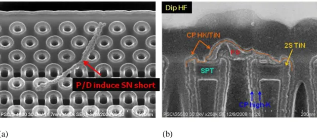
Figure 2.6 is the analysis in wafer failure test. The SEM cross-section indicates that the particle defects appear before High-K dielectric deposition but after bottom TiN electrode formation. Thus, it is proofs that these particle defects comes from crown wet capacitor etch process from wet bench.
(a)
(b)
Figure 2.5 (a) Failure map versus in-line defect map of lot A; wafer notch pointed to bottom of wet bath tank during crown wet etch back process. (b) Failure map versus in-line defect map of lot B; wafer notch pointed to top of wet bath tank during crown wet etch back process.
24
(a) (b)
Figure 2.6 (a) Top view of particle defect induced capacitor short (b) Cross section of particle defects appear before high-K dielectric deposition and after bottom TiN electrode formation.
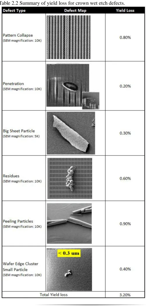
2.4.2 Summary of Yield Loss for Each Defect Categorization
All defects including pattern collapse, particles and residues after the crown wet etch process are taken into account the yield loss. 250 wafers together with defects and wafer yield data are compared and analyzed. The average yield loss is predicted. Table 2.2 summarizes the correlation of each defect type after crown wet etch to the yield loss. However, pattern collapse and penetration which caused 1 percent of yield loss will not be focused on this study. This study will focus generally on the particle removal ability: how to remove big sheet particles, residues, peeling particles and wafer edge cluster, small particles, that totally impact 2.2 percent of wafer yield loss will be evaluated.
26
2.5 Particle Adhesion in a Liquid Bath
To understand the particle detachment from the wafer surface, it is essential to understand the particle adhesion on the wafer. This section will briefly introduce three key parameters that contribute to the deposition and detachment of particles on the wafer surface. After the treatment of concentrated HF on the crown wet capacitor, hydrophobic surface is considered in the following discussion.
2.5.1 Zeta Potential
Particles dispersed or suspended in a liquid system are called colloids. Colloids typically acquire an electrical charge when immersed in a liquid medium [4]. Charge on a colloid is often measured in terms of a zeta potential, the potential at the shear plane between the colloid and the liquid. A typical charge distribution surrounding a colloid is sketched in Figure 2.7 [5]. Electrical potential at the colloid surface is maximum and decreases through the surrounding layers of excess positive ions until reaching the value of the bulk solution where equilibrium concentrations of positive and negative ions exist.
Relative motion of the colloid with respect to the solution divides the positive ion sheath into two regions: (i) the ion region near the charged colloid that moves with the colloid; and (ii) the diffuse region remote from the colloid which moves with the bulk liquid. The boundary between these two regions is the shear plane, and the potential at this shear plane is called zeta potential.
28
Figure 2.7 Electrostatic double layer around a particle [5].
(net) Electro- Negative Particle Nernst Potential Zeta Potential Electric Potential Surrounding the Particle Layer of Adsorbed ions Plane of Shear Extent of Diffuse Layer of Counter ions Bulk of Solution Concentration of Positive Ions Concentration of Negative Ions
In liquid, both the wafer surface and the particles acquire surface charge, which is characterized by zeta potential. It is independent of particle size but depends on the electrolyte pH: in acidic conditions (low pH) the zeta potential is positive, and in alkaline solution it tends to be negative, as shown in Figure 2.8. Like charges repel each other and opposite charges attract each other. Acid cleans, such as HF, which result in a positive zeta potential for most particles and a negative zeta potential for silicon surfaces, are therefore prone to particle adhesion [6].
Figure 2.8 Zeta potential: pH influences particle adhesion and removal [7].
2.5.2 Electric Double Layer Repulsion
The fundamental interactions occurring between particles and the wafer surface in solutions are the van der Waals force and the electrostatic force (the reciprocal action of an electrical double layer) [8].
30
If a negatively charged colloid is repelled from a negatively charged wafer surface, then it is the repulsive forces that dominate the interaction between them, no contact between them will take place and no deposition will occur. This interaction is called electrostatic double layer repulsion (EDR) [7].
The width of the diffuse layer depicted in Figure 2.7 depends on the ionic strength of the liquid surrounding the particle. At high concentration, the range of the region of excess positive charge is short because the particle charge can be balanced by only a small volume of liquid.
2.5.3 Van der Waals Attraction
Van der Waals attraction between molecules arises from an interaction between the electron clouds surrounding each molecule. The displacement in electron distributions induced by the presence of the other molecule introduces a dipolar electric force which is always attractive [9].
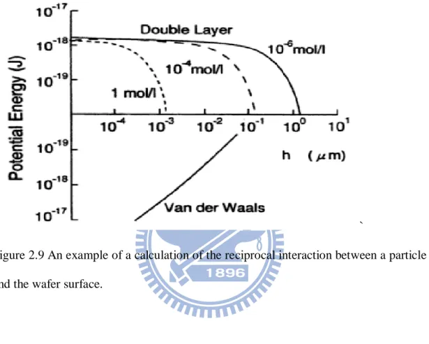
The entire reciprocal action between the particle and wafer is shown as the sum of the electrical double layer potential and the van der Waals potential; if it is positive, repulsion acts between the particle and wafer, and if it is negative, attraction. On the other hand, the electrical double layer in the vicinity of the charged suface changes according to the sphere of influence of the ion density in the solution. When the ion density in the solution increases, van der Waals attraction is superior to the electrical double layer repulsion, and particles are deposited.
surface are the same sign. When the signs are different, the electrical double layer force and van der Waals force acts as an attraction, conditions which cause particles to deposit easily.
`
Figure 2.9 An example of a calculation of the reciprocal interaction between a particle and the wafer surface.
2.5.4 DLVO Theory
The interaction energy between two particles can be represented according to the DLVO theory of colloidal stability [10][11]. The DLVO theory of colloidal stability assumes that the coagulation behavior of particles depends mainly on the van der Waals interactions energy and on the double layer interaction energy. DLVO theory suggests that the stability of a particle in solution is dependent upon its total potential energy function VT. This theory recognizes that VT is the balance of several competing
32
(Equation 2-1)
Where VS is the potential energy due to the solvent, it usually only makes a marginal
contribution to the total potential energy over the last few nanometers of separation. Much more important is the balance between VA and VR, these are the attractive and
repulsive contributions. They potentially are much larger and operate over a much larger distance.
(Equation 2.2)
Where A is the Hamaker constant and D is the particle separation. The repulsive potential VR is a far more complex function.
(Equation 2.3)
where is the particle radius, is the solvent permeability, is a function of the ionic composition and is the zeta potential.
DLVO theory suggests that the stability of a colloidal system is determined by the sum of these van der Waals attractive (VA) and electrical double layer repulsive (VR)
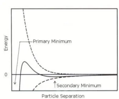
forces that exist between particles as they approach each other due to the Brownian motion they are undergoing. This theory proposes that an energy barrier resulting from the repulsive force prevents two particles approaching one another and adhering together (Figure 2.10). But if the particles collide with sufficient energy to overcome
that barrier, the attractive force will pull them into contact where they adhere strongly and irreversibly together. Therefore, if the particles have a sufficiently high repulsion, the dispersion will resist flocculation and the colloidal system will be stable. However, if a repulsion mechanism does not exist then flocculation or coagulation will eventually take place.
In certain situations (e.g. in high concentration HF), there is a possibility of a “secondary minimum” where a much weaker and potentially reversible adhesion between particles exists together (Figure 2.11). These weak forces are sufficiently stable, and can’t be broken up by Brownian motion, but may dissociate under an externally applied force such as vigorous agitation.
Figure 2.10 Schematic diagram of variation of free energy with particle separation according to DLVO theory. The net energy is given by the sum of the double layer repulsion and the van der Waals attractive forces that the particles experience as they approach one another.
34
Figure 2.11 Schematic diagram of the variation of free energy with particle separation at higher salt concentrations showing the possibility of a secondary minimum.
2.6 Conclusions
From the defect source analysis result, it is proved that the root cause of most capacitor loop electrical characteristic failure is due to crown wet etch particle defects. And these defects are mainly big sheet particles which are Ti- rich; and polymer residues which are carbon-rich and silicon-rich. Thus, a cleaning process method to remove these particles after the crown wet capacitor process will be investigated, and will be introduced in the next two chapters.
Section 2.5 introduced how these particles are attached in the HF liquid bath. The zeta potential is used to explain the particles adhesion and removal from the wafer surfaces. The DLVO theory, a combination of both van der Waals forces and electric double layer repulsion, guided the experimental methods chosen in the next chapter.
References
1. Hiroshi M., Akinobu T., Hitoshi M., Senri O., Kenichi M., “High-Performance Wet Cleaning Technology”, Scientific Wet Process Technology for Innovative LSI/FPD Manufacturing, Ed. 2006, USA.
2. T. Hattori, Sony, "Contamination Control: Problems and Prospects", Solid State Technology , vol.33, no.7, pp. S1-S8, 1990.
3. Jun Sugiura, "Influence of Contaminants on Device Characteristics", Ultraclean Surface Processing of Silicon Wafers, Springer, Ed. 1998, Japan.
4. K.Werner, “Handbook of semiconductor wafer cleaning technology: science, technology, and applications”, Noyes Publications, Ed. 1993, USA.
5. Ranade, M.B., “Adhesion and removal of fine particles on surfaces”, Aerosol Science & Technology, volume 9, pp.179-191, 1987.
6. Franssila, S., “Introduction to microfabrication”, J.Wiley, Ed. 2004, USA.
7. M. Itano, F.W. Kern, Jr., I. Kawanabe, M. Miyashita, R.W. Rosenberg, and T. Ohmi, “ Particle removal from silicon wafer surface in wet cleaning process”, IEEE transactions on Semiconductor Manufacturing, Volume 6, issue 3, pp.258-267, 1993.
8. M. Itano, T. Kezuka, “Particle adhesion and removal on wafer surfaces in RCA cleaning”, Ultraclean Surface Processing of Silicon Wafers, Springer, Ed. 1998, Japan.
9. D.S. Rimai, L.P. Demejo and R.C. Bowen, “Mechanics of particle adhesion”, Fundamentals of Adhesion and Interfaces, pp.1-23, 2004.
10. B.V. Derjaguin and L.D Landau, “Theory of the stability of strongly charged hydrophobic sols and of the adhesion of strongly charged particles in solutions of electrolytes”, Acta Physicochim USSR, Volume:14, pp. 633, 1941.
36
11. E.J.W. Verwey and J.T.G. Overbeek, “Theory of the Stability of Hydrophobic Colloids.”, Amsterdam, Elsevier, pp. 118, 1948.
12. C. Ruggiero, M. Mantelli, A.Curtis, S.Zhang, P. Rolfe, “A computer model of the adhesion behaviour of particles under the influence of DLVO and hydrophobic interactions”, Proceedings of the 20th Annual International Conference of the IEEE Engineering in Medicine and Biology Society, vol 6, pp.2838-2841, 1998.
Chapter 3: Process Parameters and Analysis
Methods
As stated in chapter 2, particulate defects with a size bigger than 0.5 µm prove to have a direct yield loss on 68nm generation DRAM device. These kinds of particulate defects are in fact a consequence of a variation in surface properties and a result of a series of process steps. A cleaning process has to be performed in order to remove these particles. How these particles can be removed is a worthwhile study, since the conventional methods of intensive megasonic irradiation for contaminant de-absorption and for etching of the underlying film by as much as several nanometers can be no longer applied. This is because pattern collapses and dimensional fluctuation due to the etching have become critical [1]. Therefore, a series of cleaning experiments which comprise of single wafer equipment and batch type spray process equipment were undergone in order to get a clean surface after the capacitor crown wet process.
3.1 Processing Tools and Steps
The fabrication of DRAM devices encompassed a number of treatments, such as film deposition, photolithography, cleaning and etching steps. The facility included in this study is a Class-100 clean room (Figure 3.1). A Class-100 clean room maintains less than one hundred particles larger than 0.5 micron meter in each cubic foot of air space. The process step to be investigated will focus on the wet cleaning step after the crown wet capacitor formation. It is essential yet difficult to remove the residues and defects from the bottoms of cylinder holes as well as from the wafer surface. Otherwise, the
38
gap fill of the upper capacitor electrode will be unstable, resulting in both performance and functional yield losses [2,3] . To be compatible with this study, the following processing tools were chosen .
1. Single Wafer Type Tool (SEZ DV38-DS). 2. Batch Type Spray Process Tool (TEL PR300z).
Figure 3.1: Class-100 Clean Room.
3.1.1 Processing Tool: Single Wafer Type Tool
Designed with the 300mm wafer Da Vinci ™ platform, SEZ DV38-DS offers eight double-sided process modules; enabling simultaneous, high-throughput removal of wafer front-side polymers and backside organics or particles (Figure 3.2). The process takes place in a multilevel process chamber. The chemistry is dispensed onto the top wafer surface or simultaneously onto both wafer surfaces at one level. Then, the wafer
is moved to another process level where it is rinsed with DI water and dried. This approach isolates the wafer frontside and backside, eliminating cross-contamination between wafer surfaces [3] (Figure 3.3).
40
Figure 3.3: Schematic of SEZ DV 38-DS process chamber.
3.1.2 Processing Tool: Batch Type Spray Process Tool
Although batch type spray process tool cleaning has been a mature technology for wafer cleaning for many years, there are still advancements made today, especially targeted for the 60nm and below technology node. According to an article presented by FSI on Semiconductor Manufacturing Magazine [4], centrifugal batch spray systems have successfully demonstrated higher particle removal efficiencies compared to non-megasonic wet benches, due to greater hydrodynamic forces. The other advantages for IC manufacturers, like leverage cost and cycle time reduction, also consolidate its role in semiconductor wet cleaning technology.
The batch type spray process tool, TEL PR300z, from Tokyo Electron Limited, Akasaka, Japan, that is commonly used for stripping photoresist from 12 inch wafers
for back end of line (BEOL) processing is used in this work (Figure 3.4). TEL PR300z has one process chamber with a maximum 25 wafers processing.
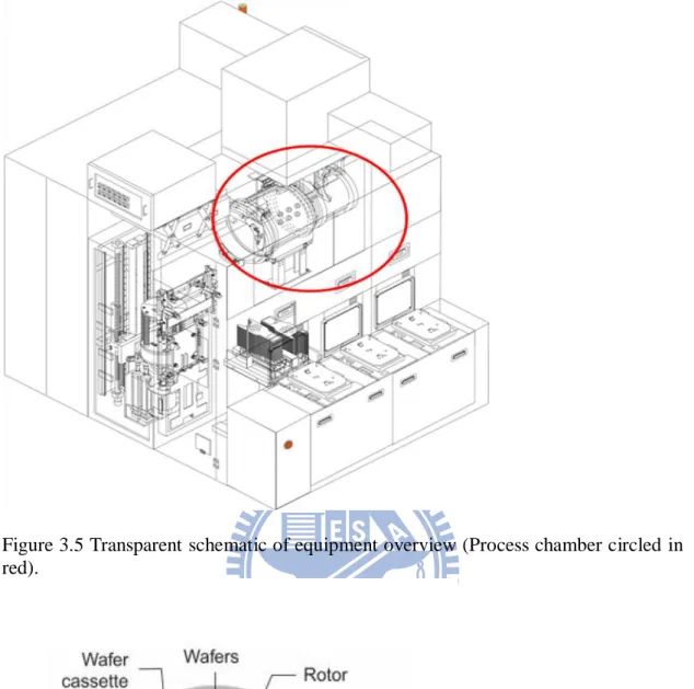
The TEL PR300z process chamber can be divided into an inner and outer chamber. The inner chamber nozzle is responsible for spraying chemicals, rinsing IsoPropanol (IPA) & gas nitrogen (N2). Meanwhile, as for the function of the outer chamber nozzle,
it uses DI water clean to rinse and Nitrogen gas to dry (Figure 3.5). During the cleaning process, the process rotor will rotate a maximum of 25 wafers. The chamber nozzles will remain static while the wafers are rotating (Figure 3.6 & Figure 3.7).
42
Figure 3.5 Transparent schematic of equipment overview (Process chamber circled in red).
Figure 3.7 Schematic of TEL PR300z process chamber cross-section.
3.1.3 Processing Steps
This work emphasizes ways and methods to remove particles and residues generated from the oxide etch crown capacitor process. Thus, the investigative process steps include:
1. Crown capacitor wet etch.
2. Polymer residues and particles removal.
3.2 Sample Preparation
As substrates, one-sided polished silicon wafers are chosen with a thickness of 775μm and a diameter of 300 mm. Transistors are well formed, and bottom Titanium Nitride (TiN) electrodes on crown-shaped capacitors are integrated on top of a contact landing pad. The critical dimension of the capacitor is 0.091µm in diameter and 1.7µ m in height, corresponding to the aspect ratio 18.7 as illustrated in Figure 3.8(a). Figure
Motor Spin shaft Inner nozzle Outer nozzle Chamber wall Inner Drain Outer Drain 25 wafers
44
3.8(b) to Figure 3.8(d) show the exact image of the crown capacitor from a SEM cross-section view. The capacitor cylinders with TiN bottom electrodes exposed, are supported with 50 nm Si3N4 film on the top of the cylinders open area. This
architecture work of the crown-shaped capacitor stands solidly on a tungsten (W) landing pad which functions as the contact. The relevant process is presented in Chapter 1, Figure 1.1.
(a) (b)
(c) (d) Figure 3.8
(a) SEM cross-section view of crown-shaped capacitor (50 K magnification). (b) Schematic of crown-shaped capacitor architecture.
(c) Bottom of crown-shaped capacitor, contact with W landing pad (100 K magnification).
(d) Top-side of crown-shaped capacitor, support-Si3N4 structured to prevent capacitor
46
3.2.1 Crown Capacitor Wet Etch Process
A wet bench tool, TEL UW300z (Figure 3.9) was chosen to perform the crown capacitor wet etch process. 49 wt% hydrogen fluoride (HF) with a temperature 20 degrees°C and circulation flow rate of around 23 liters/min is used to etch off ILD (Inter-Layer Dielectric). The main purpose of using 49 wt% HF is due to its high selectivity of various ILD films. The selectivity of Si3N4 to PSG is 1 to 65 tested on
non-pattern film wafers. As a consequence of using pure HF solution, exposed ILD films are etched off completely; meanwhile partial amount of Si3N4 film will remain
to support the cylinder capacitor. The remaining Si3N4 film is called the supporting-
Si3N4 structure. The supporting- Si3N4 plays the important role of keeping the crown
cylinders from collapsing (Figure 3.8 d ).
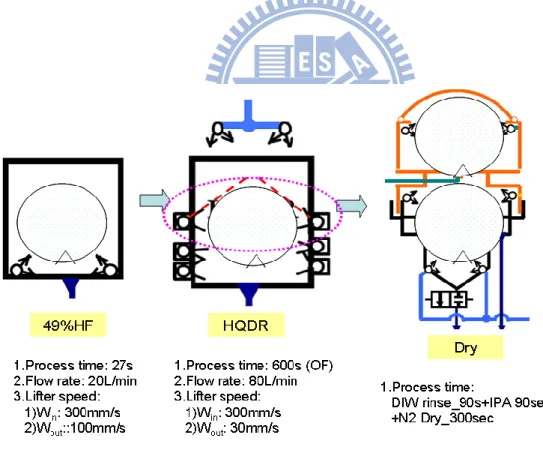
To be accessible with clean room facilities and equipment tank configuration, two conditions are designed in order to prepare a defect-less sample.
1. 49 wt% hydrogen fluoride (HF), 20 degrees°C, 20 liters/minute , 27 seconds DI water rinse, 80 liters/minute, 600seconds IPA 90 seconds + N2 300 seconds dry
(as illustrated in Figure 3.9).
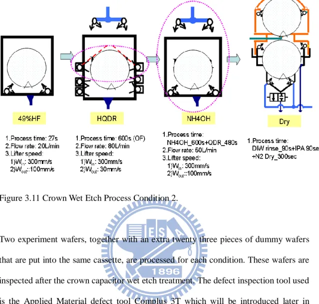
2. 49 wt% HF, 20 degrees°C, 20 liters/minute , 27 seconds DI water rinse, 80 liters/minute, 600 seconds 1:200 NH4OH:H2O, Room Temperature, 600
seconds IPA 90 seconds + N2 300 seconds dry (as illustrated in Figure 3.10).
48
Figure 3.11 Crown Wet Etch Process Condition 2.
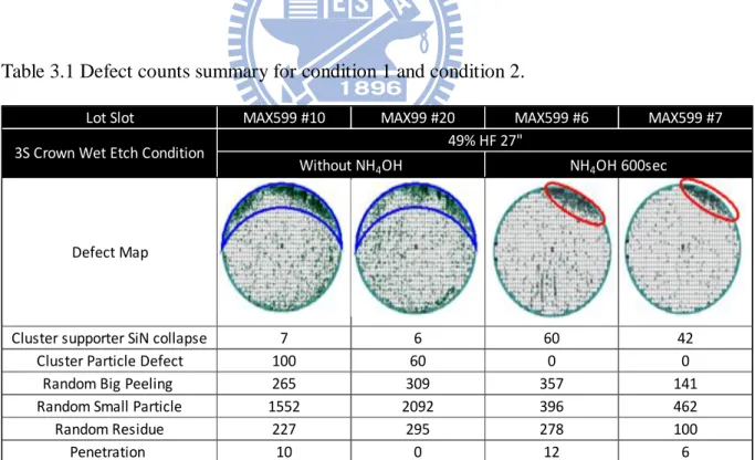
Two experiment wafers, together with an extra twenty three pieces of dummy wafers that are put into the same cassette, are processed for each condition. These wafers are inspected after the crown capacitor wet etch treatment. The defect inspection tool used is the Applied Material defect tool Complus 3T which will be introduced later in Section 3.6.
From Table 3.1, two different defect maps appeared. The result of the defect inspection is divided into seven categories, which included a cluster type cylinder supporting Si3N4 peelings defect; cluster type particles; random distribution big
peeling particles; random distribution small particles with size smaller than 0.5µ m; random distribution organic type residues and penetration. The scanned defects are classified into these categories accordingly. Without NH4OH treatment, defects are
defined as having more than 100 particles, with a size larger than 0.1µ m per die, distribute most near the surface of the wafer edge. Then, without NH4OH treatment,
wafers contain 400 percent more random small particles (particles with size smaller than 0.5µ m) than those with NH4OH treatment. Figure 3.12 shows the SEM image for
particle categories that mentioned earlier.
Table 3.1 and Graph 3.1 show that wafers with NH4OH treatment have better
performance than ones without. NH4OH solution has changed the zeta potential on the
particles and the wafer surface, which enhances the effect of particle removal. In order to get a better wafer yield, wafers with NH4OH treatment were chosen for the next
experiment.
Table 3.1 Defect counts summary for condition 1 and condition 2.
Lot Slot MAX599 #10 MAX99 #20 MAX599 #6 MAX599 #7
Defect Map
Cluster supporter SiN collapse 7 6 60 42 Cluster Particle Defect 100 60 0 0
Random Big Peeling 265 309 357 141 Random Small Particle 1552 2092 396 462 Random Residue 227 295 278 100 Penetration 10 0 12 6
Without NH4OH NH4OH 600sec
50
Crown Wet Condition versus Defect Count
0 500 1000 1500 2000 2500 Cluster supporter SiN collapse Cluster Particle Defect Random Big Peeling Random Small Particle Random Residue Penetration defect type Cou nts/Dies #10 without NH4OH #20 Without NH4OH #6 NH4OH 600sec #7 NH4OH 600sec
Graph 3.1 Defect counts for condition 1 and condition 2.
(a) (b) (c) (d)
Figure 3.12 (a) cylinder supporter collapse (b) small particle (<0.5μm) (c) big particle (>0.5μm) (d) residue. (SEM 10K magnification)
3.3 Experimental Design: Single Wafer Type Tool
The surface material of the specimen exposed is mainly Titanium, therefore, strong oxidation chemicals and concentrated acids are avoided. The most noted chemical property of titanium is its excellent resistance to corrosion, capable of withstanding attack by dilute sulfuric acid and hydrochloric acid as well as chlorine gas, chloride solutions, and most organic acids. Thus, dilute chemicals are targeted. And in order to be compatible with Perfluoroalkoxy (PFA) copolymer resin material in SEZ DV38-DS experimental tool, chemicals EKC6800 and Rezi-38 are chosen to be investigated. The single-wafer spin processor rinses from the wafer center to the edge, there are fewer inherent defectivity transfer pathway.
3.3.1 Chemical Selection :
3.3.1.1 EKC6800 [5]
EKC technology, Inc., part of DuPont Electronic and Communications, is the leading manufacturer of patent specialty chemicals used in the manufacturing of wafers for the semiconductor and related industries. EKC6800, one of the chemicals used in the Back End of Line (BEOL) for advanced interconnect applications was chosen in this experiment. EKC6800 contains 55~85 percent of N,N-Dimethylacetamide and 0~5 percent of Ammonium bifluoride, and with a pH value varied from 6 to 8. The main reason for this chemical being chosen is that, the contained fluoride can react with polymer residues. Polymer residues are then reformed into a low molecular structure that is soluble in water.
52
3.3.1.2 Rezi-38 [6]
Rezi-38, a product of Baker Incorporate, is an aqueous ash residue remover, which effectively cleans a wide variety of metal-organic residues from substrates, including sensitive metal alloys like copper and low k dielectrics. With a pH around 13, this product is 80 percent aqueous, which requires no special rinse and is effective at room temperatures (as low as 23 degrees°C). In addition, Rezi-38’s aqueous composition also offers a variety of environmental benefits. It does not contain SARA 313[7] specified components or hazardous air pollutants (HAPs), and has a less than 5 percent concentration of volatile organic compounds (VOCs). In addition, the high water content of the product allows easier disposition that is environment free. Table 3.2 below compares Rezi-38 and EKC6800.
Table 3.2 Comparison of REZI-38 and EKC 6800 chemicals.
Chemical REZI-38 EKC 6800
Maker Baker Dupont
Formulation >85% Aqueous <3% TMAH Fluoride salt Organic solvent Acid/base pH Viscosity @ RT Solubility in Water Surface Tension Base 13 1.2 cSt. Complete 72 dyne/cm Alkalescent 7.8 ~ 8.2 --- Complete --- Etch Rate (A/min)
TiN W Ti ~0 2.3 0.103 0 0.41 0
54
3.4 Experimental Design: Batch Type Process Tool
As stated above, the majority of defect particles distributed are Titanium rich compounds. We targeted a few chemicals that are compatible with the equipment material, that is stainless steel SUS 316 that has a good resistance to heat and corrosion : EKC265[8], ELM C30[9] and EcoPeeler [10].
3.4.1 Chemical Selection : EKC265, ELM C30 & EcoPeeler
3.4.1.1 EKC265 [8]
Also invented by EKC technology, Inc., EKC265 is the initial product of Dupont™ PlasmaSolv® series formulated to remove photoresist residue generated after via and metal etch processes. EKC265 post-etch residue removers are made with Hydroxylamine (HDA) high performance hydroxylamine-based cleaning technology. HDA technology comprises aqueous organic mixtures formulated to effectively remove residues from substrate surfaces after via, poly and metal etch processes used in the microelectronics industry.
3.4.1.2 ELM C30 [9]
A product of Mitsubishi Gas Chemicals, the ELM series cleaning chemical specialize in cleaning and removing etch residue with inorganic chemicals. However, ELM C30 contains Dimethylformamide (DMF) as a chemical solvent. Dimethylformamide is the organic compound with the formula (CH3)2NC(O)H which is a common solvent
for chemical reactions, unfortunately, this is always linked to cancer in humans, and is also thought to cause birth defects.
3.4.1.3 EcoPeeLer[10]
EcoPeeler is a transparent and inorganic chemical which does not contain any HDA (Hydroxylamine), hazardous, toxic or organic solvents. A product of Fine Polymer, the pH of EcoPeeler can be controlled to required levels so as to be comparable with various processes. It is also a cost effective chemical as there is no necessity for additional facilities or cost associated with its disposal. But most important of all, EcoPeeler is eco-friendly and provide a low CoO (Cost of Ownership) advantage.
Table 3.3 summarizes the differences between these three chemicals for batch type spray process tool.
56
Table 3.3 Comparison of batch type spray tool chemical.
Chemical EKC265 ELM C30 EcoPeeler
Maker Dupont MGC Fine Polymers
Formulation 1) 2-(2-aminoethox y)ethanol 50~100% 2) Hydroxylamine (HDA) 10~25% 3) Pyrocatechol 2.5~10% 1) Dimethylformami de (DMF) 69% 2) Fluoride compound 2% 3) Water 29% 1) Ammonium phosphate (NH3H2PO) 2) Condensed ammonium phosphate (-(OPNH3)n-) 3) Urea (OC(NH2)2) 4) Water Acid/base pH Solubility in Water Base 11.5~12.5 Completely Neutral 7~8 Completely Acid 3~4 Well Mixed Etch Rate (A/min) TiN W Ti TEOS 2.0 0.7 34.2 0.1 0.7 1.9 3.6 197 0.9 0.3 5.4 0.1
![Table 1.1 Typical cleaning solutions used in the semiconductor manufacturing process [10]](https://thumb-ap.123doks.com/thumbv2/9libinfo/8262950.172265/25.892.129.760.461.726/table-typical-cleaning-solutions-used-semiconductor-manufacturing-process.webp)