具有基體偏壓之低雜訊放大器及整合型多相位濾波器之1-V 2.4-GHz低中頻架構前端接收器電路設計
91
0
0
全文
(2) 具有基體偏壓低雜訊放大器及整合型多相位濾波器之 1-V 2.4-GHz 低中頻架構前端接收器電路設計 The Design of 1-V 2.4-GHz Low-IF Receiver Front-End With Body-biased Low Noise-Amplifier and Integrated Polyphase Filter 研 究 生:吳瑞仁. Student:Jui-Jen Wu. 指導教授:吳重雨. Advisor:Chung-Yu Wu. 國立交通大學 電機資訊學院 電子與光電學程 碩士論文. A Thesis Submitted to Degree Program of Electrical Engineering Computer Science College of Electrical Engineering and Computer Science National Chiao Tung University in Partial Fulfillment of the Requirements for the Degree of Master of Science in Electronics and Electro-Optical Engineering June 2004 Hsinchu, Taiwan, Republic of China 中華民國九十三年十二月.
(3) 授權書. (博碩士論文) 本授權書所授權之論文為本人在__國立交通____大學(學院)_電子__系所 _電子與光電__組_九十三_學年度第_一_學期取得_碩__士學位之論文。 論文名稱:具有基體偏壓之低雜訊放大器及整合型多相位濾波器之 1-V 2.4-GHz 低中頻架構前端接收器電路設計 1.■同意 □不同意 本人具有著作財產權之論文全文資料,授予行政院國家科學委員會科學技術資料中心、 國家圖書館及本人畢業學校圖書館,得不限地域、時間與次數以微縮、光碟或數位化等 各種方式重製後散布發行或上載網路。 本論文為本人向經濟部智慧財產局申請專利的附件之一,請將全文資料延後兩年後再公 開。(請註明文號: ) 2. ■同意 □不同意 本人具有著作財產權之論文全文資料,授予教育部指定送繳之圖書館及本人畢業學校圖 書館,為學術研究之目的以各種方法重製,或為上述目的再授權他人以各種方法重製, 不限地域與時間,惟每人以一份為限。 上述授權內容均無須訂立讓與及授權契約書。依本授權之發行權為非專屬性發行權利。依本 授權所為之收錄、重製、發行及學術研發利用均為無償。上述同意與不同意之欄位若未鉤 選,本人同意視同授權。 指導教授姓名:吳重雨. 研究生簽名: (親筆正楷) 日期:民國. 學號:8967514 (務必填寫) 94 年. 12. 月. 28. 日. 1. 本授權書請以黑筆撰寫並影印裝訂於書名頁之次頁。 2. 授權第一項者,所繳的論文本將由註冊組彙總寄交國科會科學技術資料中心。 3. 本授權書已於民國 85 年 4 月 10 日送請內政部著作權委員會(現為經濟部智慧財產局) 修正定稿。 4. 本案依據教育部國家圖書館 85.4.19 台(85)圖編字第 712 號函辦理。.
(4) 國立交通大學 論文口試委員會審定書 本校 電機資訊學院專班. 電子與光電. 組 吳瑞仁. 君. 所提論文 (中文). 具有基體偏壓之低雜訊放大器及整合型多相位濾波器 之 1-V 2.4-GHz 低中頻架構前端接收器電路設計. (英文). The design of 1-V 2.4-GHz Low-IF Receiver front-end with body-biased low noise- amplifier and integrated polyphase filter. 合於碩士資格水準、業經本委員會評審認可。. 口試委員:. 吳重雨. 、. 洪崇智. 謝志成. 、. 林明仁. 指導教授: 吳重雨 博士 班主任: 中 華 民 國. 93. 年 12 月 28 日.
(5) 具有基體偏壓之低雜訊放大器及整合型多相位濾波器之 1-V 2.4-GHz 低中頻架構前端接收器電路設計. 學生:吳瑞仁. 指導教授:吳重雨 教授. 國立交通大學電機資訊學院 電子與光電學程﹙研究所﹚碩士班. 摘. 要. 此論文提出一個能操作在 1-V 電源電壓,射頻頻率為 2.4-GHz 之低中 頻架構之前端接收器電路,所完成的晶片是一個適用於電池供電的通訊器或 藍芽無線傳輸的應用。目的是能夠實現一個簡單,低成本,低電壓,低功率 消耗,且能有最少的額外元件,而能夠很容易的使用在可攜式裝備上。 這個晶片的製作是透過國家晶片系統設計中心,以台灣積體電路製造 股份有限公司提供的 0.25-um 互補式金氧半導體製程技術實現。整個晶片 包含一個基體偏壓型低雜訊放大器,正交壓控振盪器,降頻混波器及一個主 動型多相位濾波器。 量測結果顯示,接收器可以正確的操作在 1-V 電源電壓。它並能提供 15-dB 增益,17-dB 的雜訊指數,41-dB 的鏡像拒斥比,-15-dBm 輸入三階 截點值。在 1-V 電源電壓下有 18.575mW 的功率消耗。. i.
(6) The Design of 1-V 2.4-GHz Low-IF Receiver Front-End With Body-biased Low-Noise Amplifier and Integrated Polyphase Filter. Student:Jui-Jen Wu. Advisors:Prof. Chung-Yu Wu. Degree Program of Electrical Engineering Computer Science National Chiao Tung University. ABSTRACT This thesis proposed a design of 1-V 2.4-GHz low-IF architecture receiver front-end circuit. It is suitable for battery-based communication equipments or bluetooth application. The goal of this design is to realize a simple, low cost, low voltage, low power consumption and with fewer external components receiver architecture and it can be easy to use for portable equipments. This chip was fabricated using 0.25-um CMOS technology provided by Taiwan semiconductor manufacturing company via national chip implementation center. Whole chip includes a body-biased low noise amplifier, quadrature voltage control oscillator, downconvert mixer and an active polyphase filter. The measured results show that the receiver can be correctly operated at 1-V power supply. The receiver provides gain 15-dB, 17-dB noise figure, 41-dB image rejection ratio, and -15-dBm input third intercept point. The power dissipation is 18.575mW with 1-V power supply.. ii.
(7) ACKNOWLEDGMENTS First, I express my deepest gratitude to my advisor, Professor Chung-Yu Wu for his enthusiastic, patient direction and invaluable suggestions. I thank to senior Dr. Hong-Sing Kao, Mr. Chung-Yun Chou and Mr. Wenchieh Wang for their kindly assistance and their useful guidance in the experience sharing of RF IC design. I also thank to my classmates Fang-Te Su, Yen Ting, Chin-Hao Chang, Chien-Hsiang Chen and Chih-Yuan Hsieh. They are good friends of mine and they always enthusiastically share their experience of RF IC design and testing methodology. In this chip’s implementation, I want to say thank to National chip implementation center (CIC), Taiwan semiconductor manufacturing company (TSMC) for their help and support in the chip fabrication. I thank my parents, who gave me the courage to get my education, supported me in all achievements. In addition, I give my dearly thanks to my wife, Yu-Pin Huang. We married last year-end. But I sacrificed a lot of time for my job and my research. Especially she born my daughter during my education, she must tolerate many pressures and take cares our baby lonely. Finally, I would like to say thank to all the people who have ever helped me in the past years.. iii.
(8) Contents Chinese Abstract English Abstract Acknowledgments Contents Table Captions Figure Captions. ………………………………………………… i ………………………………………………… ii ………………………………………………… iii ………………………………………………… iv ………………………………………………… vi ………………………………………………… vii. CHAPTER 1 INTRODUCTION ............................................................1 1.1 BACKGROUND .............................................................................................1 1.2 REVIEW CMOS RF RECEIVER ARCHITECTURES..................................3 1.2.1 Low-IF receiver with image reject filter...............................................9 1.2.2 Body-biased low-noise amplifier design ............................................10 1.3 Motivation......................................................................................................12 1.4 Thesis organization ........................................................................................12. CHAPTER 2 CIRCUIT ARCHITECTURE AND SIMULATION RESULTS .......................................................................13 2.1 SYSTEM ARCHITECTURE ........................................................................13 2.2 OPERATIONAL PRINCIPLE ......................................................................14 2.3 CIRCUIT DESIGN........................................................................................18 2.3.1 Body-biased low noise amplifier (LNA) ............................................18 2.3.2 Quadrature voltage control oscillator..................................................30 2.3.3 Quadrature mixer ................................................................................33 2.3.4 Active polyphase filter........................................................................35 2.4 RECEIVER REALIZATION ........................................................................42 2.5 SIMULATION RESULT...............................................................................44. iv.
(9) CHAPTER 3 EXPERIMENT RESULTS ..........................................53 3.1 Layout Description.........................................................................................53 3.2 Testing Description........................................................................................56 3.3 Measurement Setup........................................................................................59 3.4 Experimental results.......................................................................................62. CHAPTER 4 CONCLUSIONS AND FUTURE WORKS ................73 4.1 CONCLUSIONS............................................................................................73 4.2 FUTURE WORKS.........................................................................................74. REFERENCES ......................................................................................75. v.
(10) Table Captions CHAPTER 1 INTRODUCTION ............................................................1 CHAPTER 2 CIRCUIT ARCHITECTURE AND SIMULATION RESULTS ......................................................................13 Table 2.1 LNA device parameter.........................................................................29 Table 2.2 QVCO device parameter......................................................................32 Table 2.3 Mixer device parameter .......................................................................35 Table 2.4 Compare with passive and active polyphase filter...............................40 Table 2.5 The comparison between w/o body bias, w/i body bias.and reference paper.....................................................................................................46 Table 2.6 The performance summary of polyphse filter......................................51 Table 2.7 The gain and noise figure assignment..................................................52. CHAPTER 3 EXPERIMENT RESULTS ..........................................53 Table 3.1 DC bias tables ......................................................................................62 Table 3.2 Final summaries of measurement results.............................................71 Table 3.3 Measured performances compared with Bluetooth specifications ......72 Table 3.4 Receiver comparisons with another quadrature-designed receiver .....72. CHAPTER 4 CONCLUSIONS AND FUTURE WORKS ................73. vi.
(11) Figure Captions CHAPTER 1 INTRODUCTION ............................................................1 Fig. 1.1 RF technology trend (TSMC)...................................................................2 Fig. 1.2 transceiver system architecture.................................................................3 Fig. 1.3 Heterodyne architecture............................................................................5 Fig. 1.4 Direct conversion architecture..................................................................7 Fig. 1.5 DC offset due to self-mixing of LO..........................................................7 Fig. 1.6 Effect of second-order distortion..............................................................8 Fig. 1.7 Low-IF architecture with polyphase filter ................................................9. CHAPTER 2 CIRCUIT ARCHITECTURE AND SIMULATION RESULTS ......................................................................13 Fig. 2.1 System architecture.................................................................................13 Fig. 2.2 Operation of downconversion ................................................................15 Fig. 2.3 IF quadrature I/Q signal generator..........................................................16 Fig. 2.4 Low-IF quadrature downconverter.........................................................16 Fig. 2.5 Single end cascode NMOS place on Deep N-well with body-bias ........19 Fig. 2.6 Cross section of cascode NMOS place on deep N-well .........................19 Fig. 2.7 The deviation of threshold voltage and forward current ........................20 Fig. 2.8 body-bias voltage vs. LNA gain .............................................................21 Fig. 2.9 LNA gain with difference body-bias ......................................................22 Fig. 2.10 (a) Resistive termination (b) 1/gm termination (c) shunt-series feedback (d) inductive degeneration....................................................23 Fig. 2.11 The small signal model of Input impendence matching.......................23 Fig. 2.12 Parasitic circuit model of a pad capacitance and bond-wire ................25 Fig. 2.13 LNA Gmeff small signal analysis equivalent circuit............................25. vii.
(12) Fig. 2.14 small signal noise model of MOS device .............................................26 Fig. 2.15 Equivalent gate circuit ..........................................................................27 Fig. 2.16 Revised Noise model ............................................................................27 Fig. 2.17 LNA circuit...........................................................................................29 Fig. 2.18 Typical RLC tank .................................................................................30 Fig. 2.19 Conceptual block diagram of the quadrature VCO ..............................31 Fig. 2.20 Fully differential inverter with LC-tuned in the quadrature VCO........31 Fig. 2.21 The whole circuit of quadeature voltage-controlled oscillator circuit..32 Fig. 2.22 Basic PMOS unit cell of mixer.............................................................33 Fig. 2.23 Mix Va and Vb operation constructed by two basic PMOS device .....34 Fig. 2.24 double-balanced mixer structure ..........................................................34 Fig. 2.25 Quadrature downconversion mixer schematic .....................................35 Fig. 2.26 4-stages RC network polyphase filter...................................................36 Fig. 2.27 The principle of complex filter.............................................................37 Fig. 2.28 Using real filter realize complex filter..................................................38 Fig. 2.29 The four-stage polyphase filter.............................................................38 Fig. 2.30 Polyphase filter input bias. ...................................................................39 Fig. 2.31 1-stage polyphase filter.........................................................................39 Fig. 2.32 4-stage polyphase filter.........................................................................39 Fig. 2.33 output buffer .........................................................................................40 Fig. 2.34 whole chip of receiver schematic .........................................................43 Fig. 2.35 simulated voltage gain of the LNA.......................................................44 Fig. 2.36 The simulated input matching (S11) of the receiver ............................45 Fig. 2.37 (a) LNA P-1dB HSPICE simulation result. (b) redesign the LNA gain to 6dB, P-1dB can be improved to -5.5dBm........................................45. viii.
(13) Fig. 2.38 LNA noise figure SpectreRF simulation [email protected] ..........46 Fig. 2.39 The simulated tuning range of VCO.....................................................47 Fig. 2.40 Mixer noise figure SpectreRF simulation [email protected] Fig. 2.41 The transient analysis of downconverter (a) input and output of LNA (b) I/Q signal of quadrature VCO (c) output waveform of downconverter......................................................................................49 Fig. 2.42 The frequency response of polyphase filter..........................................50 Fig. 2.43 The input stage HP filter.......................................................................51 Fig. 2.44 The spectrum analysis of receiver ........................................................52 Fig. 2.45 Output noise spectral density for receiver NF=8.2dB@10MHz ..........52. CHAPTER 3 EXPERIMENT RESULTS ..........................................53 Fig. 3.1 The receiver chip layout .........................................................................55 Fig. 3.2. Die photograph and receiver chip floorplan ..........................................57 Fig. 3.3 Bonding board for the receiver...............................................................58 Fig. 3.4 test platform for receiver ........................................................................60 Fig. 3.5 The measurement setup of receiver chip ................................................61 Fig. 3.6 IIP3 and conversion gain measurement setup ........................................61 Fig. 3.7 bias conditions ........................................................................................62 Fig. 3.8 The input matching (S11) of receiver.....................................................63 Fig. 3.9 The receiver output spectrum .................................................................64 Fig. 3.10 Output spectrum of IF signal ................................................................65 Fig. 3.11 The spectrum of LO leakage ................................................................65 Fig. 3.12 The tuning range of VCO .....................................................................66 Fig. 3.13 Output spectrum of two-tone test. ........................................................67 Fig. 3.14 Two-tone-test plot for IIP3 ...................................................................67. ix.
(14) Fig. 3.15 The receiver gain with difference body-bias ........................................69 Fig. 3.16 The performance of receiver gain.........................................................70 Fig. 3.17 The performance of image rejection....................................................70. CHAPTER 4 CONCLUSIONS AND FUTURE WORKS ................73. x.
(15) CHAPTER 1 INTRODUCTION. CHAPTER 1 INTRODUCTION 1.1 BACKGROUND Before, RF CMOS process could not be widely used, due to its complexity and instability. RF front-end circuit are usually designed and fabricated with GaAs or BiCMOS technology due to its better characteristics in the RF band. However, in recent years advances in the development of CMOS processes continues to spread. CMOS processing technology have continued to reduce the minimum channel length of MOS device, thereby increasing the transistor cut-off frequency ft. In the case of RF circuits, higher ft transistor means it can be operated at higher frequency. This parameter moves up the carrier frequency of RF system. RF CMOS processing has the benefits of low cost. The wireless communication system designer attempts to integrate RF and baseband components for cost-sensitive applications. A great amount of researches continues to improve the power efficiency and to reduce the supply voltage in RF circuit used in the present generation of wireless products. Otherwise, RF system is still needed to meet the desired gain, linearity and noise figure. These are always a challenge for a RF circuit designer. Low-IF receiver is one of popular architecture in the RF receiver front-end circuit, where off-chip IF filter is easy to implement in a single chip so that the additional power dissipation can be saved and complexity can be reduced. Otherwise, low-IF receiver architecture has fewer external components. It is the benefit of integration. Monolithic image cancellation has been always a challenge in receiver design. A low-IF receiver will suffer from an in-band image signal.. 1.
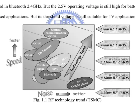
(16) CHAPTER 1 INTRODUCTION. That’s a challenging to separate the desired channel from undesired ones and from interference. The complex polyphase filter presented in this paper is the low-IF filtering section of the bluetooth in the short-range radio receiver. We used an active complex polyphase filter to restrain the image signal. This design of IF filters focus on cost, size and manufacturing point of view. Although the development of CMOS process is push to 90nm process, Fig. 1.1 is a process trend of Taiwan semiconductor manufacturing company. 0.25um CMOS process is ripe and cheaper than newer generation. 0.25um CMOS processing enhanced the ft up about to 25GHz and operating voltage is down to 2.5V(refer to TSMC’s RF IC technology). This frequency range can be easily used in bluetooth 2.4GHz. But the 2.5V operating voltage is still high for batterybased applications. But its threshold voltage is still suitable for 1V applications.. Fig. 1.1 RF technology trend (TSMC). The mail application of this thesis is used for bluetooth system. Bluetooth is an industry standard for short-range wireless voice and data communication in 2.4GHz ISM band. It regulates operating band from 2.4GHz to 2.48GHz. The channel bandwidth is about 1-MHz. In order to empower low power and highly. 2.
(17) CHAPTER 1 INTRODUCTION. integration implementations, the Bluetooth system specifications were made quite relaxed. The specification of this design is based on bluetooth. Bluetooth specifies an operating frequency range 2.40~2.48-GHz with 79 channel of 1-MHz bandwidth per channel. The basic access is based on 1-Mbps GFSK modulations. The inputpower-level range is -70~-20dBm. In this paper, the receiver was fabricated using a low cost 0.25um standard CMOS process provided by TSMC. This design used operating voltage 1V and applied in 2.4GHz bluetooth frequency band. The architecture of receiver uses a low-IF architecture with 5~10MHz intermediate frequency (IF).. 1.2 REVIEW CMOS RF RECEIVER ARCHITECTURES A typical block diagram of transceiver system is shown in Fig. 1.2. The upper side represents the receiver part of the transceiver, while the lower side represent the transmit part of transceiver. The system also includes a frequency synthesizer (RF local oscillator) to apply a clear and stable frequency. The local oscillator is responsible for the correct frequency selection in the up- and downconverters. LNA. Filter. Mixer. Filter. A/D Converter. Antenna. A/D. RF LO. ~ D/A. PA. RF Amplifier. Mixer. Filter. D/A Converter. RF band IF band Fig. 1.2 transceiver system architecture. 3.
(18) CHAPTER 1 INTRODUCTION. The frequency domain can be separated to RF band and IF band in the transceiver system. In the receive path, the receiver must be able to reject signals outside the band. The receiver must without loss and it also meet its performance. In the first stage of receiver system, the received signal amplified by the low noise amplifier (LNA). Because noise added by the LNA corrupt the received signal significantly and degrades the overall system performance, the amplifier must have the ability to detect weak signals and to reject the noise interference. Hence, noise figure is always an important consideration in the design of LNA. The received signal usually has a carrier frequency of a few 100’s MHz, or even a few GHz. The frequency down-conversion stage locks to the frequency of the received signal and down converts the received signal to the IF band. Next to the low noise amplifier, the down converter operation is done by mixing the received signal and LO signals. The LO signal is generated by a frequency synthesizer. The LO signal must be clear and stable. In the last stage of receiver, The IF band signal pass to A/D converter processing to digitize by a digital signal processor (DSP) or any application in integrated circuit. In the part of transmitter, the information signal can be speech, video or data is digitized and organized into frames. Finally, it will be transmitted by transmission path. A baseband signal is up-converted to the desired transmit carrier frequency by mixing the LO signal and IF frequency. The power amplifier transmits enough power to antenna in the last stage of transmission path. The transmitter must efficiently produce enough output power. But the harmonics will be generated in an efficient power amplifier. These usually must be filtered out before they reach the antenna.. 4.
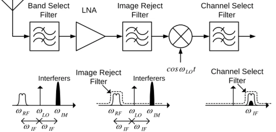
(19) CHAPTER 1 INTRODUCTION. The performance of receiver system can be issued in selectivity, noise figure, and intermodulation. High selectivity means it can receive a low magnitude signal in a high noise environment. In addition to noise consideration, a receiver system also needs enough BER (bit error rate) requirements. In order to meet this requirement, the signal must be enhanced and the noise and image signal from antenna must be degraded. The main purpose of receiver system is to translate the input RF spectrum to a much lower frequency. The primary criteria of selecting receiver architecture are their complexity, cost, integration, power dissipation and the number of external components. The designer selects receiver architecture according to their applications. The following reviews three kinds of popular receiver architectures. They are heterodyne receivers, direct-conversion receivers and Low-IF receivers. A. Heterodyne Receivers This is probably the most commonly employed architecture in current wireless communication. Heterodyne receiver down-converts the received signal to an intermediate frequency (IF). The Heterdyne receiver is illustrated in Fig. 1.3. Band Select Filter. Interferers. ω RF ωLO ω IM ω IF ω IF. LNA. Image Reject Filter. Image Reject Filter. Channel Select Filter. cos ω LO t Interferers. ω RF ωLO ω IM ω IF ω IF. Fig. 1.3 Heterodyne architecture. 5. Channel Select Filter. ω IF.
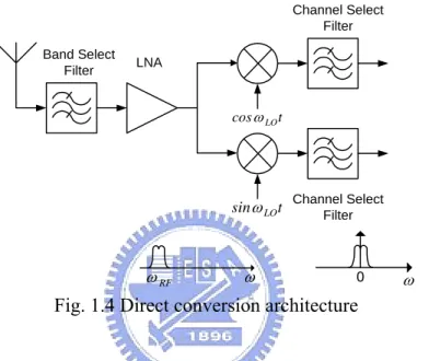
(20) CHAPTER 1 INTRODUCTION. The mixer mixes the RF signal and LO signals to generate IF. The RF frequency and LO frequency is different, and therefore the mixer output frequency is ω IF = ω RF − ω LO . If it exist an image signal ω IM to satisfy ω IF = ω LO − ω IM , they are down-convert to an identical IF. The desired signal is interfered by image signal. The receiver architecture must consider image signal ω IM and desired signal ω RF are received at the same time. For this reason, the receiver needs an image reject filter to remove the image signal. The image reject filter is usually implemented with off-chip because the filter is passive and consumes large area. Because it is off-chip implementation, the low noise amplifier must drive a 50Ω load. This intensifies a trade-off among the noise, linearity, gain and power dissipation of the low noise amplifier. Furthermore, due to it need several discrete components; the large power consumption is not suitable for low power application. There is a trade-off between the selective of IF frequency and image rejection filter. If the chosen of IF frequency is lower, the filter must have good performance reject the image frequency but the cost will be increased. If the choice of IF frequency is higher, the filter performance is relaxed. Although the heterodyne receivers widely used in most application and offer best selectivity, a number of drawbacks cause that it is difficult to implement in high-Q filter, and high power dissipation is usually not suitable for single-chip and low power application. B. Direct-Conversion Receivers Illustrate in Fig. 1.4, direct-Conversion receiver architectures translate the received signal directly to zero frequency ( ω IF = 0 ); it also called zero-IF receiver or homodyne conversion receiver.. 6.
(21) CHAPTER 1 INTRODUCTION. Compared with heterodyne architecture, direct-conversion doesn’t have the problem of image signal interference. As a result, no external image reject filter is required and the LNA need not drive a 50Ω load. Otherwise, a LPF and baseband amplifiers can replace the IF-filter in heterodyne receivers. These architectures can be easily realized to monolithic integration. Because of its simplicity, appears to offer the best opportunity for integrated systems. Channel Select Filter Band Select Filter. LNA. cos ω LO t. sin ω LO t. ω. ω RF. Channel Select Filter. 0. ω. Fig. 1.4 Direct conversion architecture The RF frequency mixes the LO frequency into baseband frequency. Image signal is shifted to negative frequency domain. The desired signal is selected by baseband LPF, therefore image signal is out of baseband domain and image signal is fully rejected.. LNA. LO Leakage. cos ω LO t. Fig. 1.5 DC offset due to self-mixing of LO Direct-conversion receiver offers many advantages to realize in monolithic integration, but it comes with a number of design issues. As shown in Fig. 1.5, DC. 7.
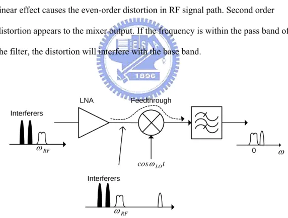
(22) CHAPTER 1 INTRODUCTION. offset is a design trouble in this architecture. The source of DC offset comes from two reasons. First, LO signal is a usually large signal and high power. LO frequency is the same as RF frequency. For this reason, LO signal is easily leak to LNA and mixer input port. The leakage effect usually arises from capacitive and subtract coupling. This leakage signal is mixed with the LO signal and produce a DC component. This DC component corrupts the baseband signal. Second, if a large interferers leaks from the LNA and mixer input to the LO port. The interferers similarly produce the DC offset variation. Another important trouble of design issue is second order distortion. As depicted in Fig. 1.6, because the transfer function of circuit is not linear, the nonlinear effect causes the even-order distortion in RF signal path. Second order distortion appears to the mixer output. If the frequency is within the pass band of the filter, the distortion will interfere with the base band.. LNA. Feedthrough. Interferers. ω RF. 0. cos ω LO t Interferers. ω RF Fig. 1.6 Effect of second-order distortion. 8. ω.
(23) CHAPTER 1 INTRODUCTION. 1.2.1 Low-IF receiver with image reject filter. Fig. 1.7 Low-IF architecture with polyphase filter Low-IF receiver is usually used in wireless communication because it’s high integrality, low cost and easy to implement filter at low frequency. The low-IF architecture resolve the trade-off between image-reject filter and channel select for IF choice. I-Q mismatch is a disadvantage of low-IF receiver. I-Q mismatch cause s the receiver unable to reject image signal entirely. Asymmetry on layout, process variation or parasitic degrades the image rejection capability. Layout and design strategies are proposed to achieve high performance of image rejection for mismatch consideration. Low-IF architecture with polyphase filter is shown in Fig 1.7, RF desired signal is amplified by low-noise amplifier and transfer to the mixer to mix with RF and LO signal. The LO signal is generated and it is I/Q signal with 90 degree phase difference. The quadrature mixer mixes the LO signal and down-convert the signal to I/Q low intermediate frequency band. This operation will be further discussion in chapter.2.. 9.
(24) CHAPTER 1 INTRODUCTION. Relative to direct-conversion receiver, the main advantage of the Low-IF receiver is that it doesn’t have DC offset problem. In order to solve the DC offset and to achieve higher monolithic integration, Low-IF receiver down converts the RF signal to IF. Although this architecture solves the troubles of DC offset, the existed image signal degrades the performance of the receiver. Fortunately, the RF signal downconverts to very low frequency and image reject filter is easy to implement at low frequency. This architecture can use many kinds of methods to reduce the image signal. For example, Hartley architecture, Weaver architecture and polyphase filter architecture. In this case of low-IF receiver, it uses a polyphase filter as the image reject filter. The basic function is used to pass the desired IF signal and to reject the image signal. The bluetooth specification is developed in favor of high-IF or low-IF architecture. However, A high IF receiver, which uses an IF much larger than the signal bandwidth, needs off-chip filters due to required high Q components. Hence the system integration level is reduced and extra power on the I/O driving circuit is demanded. In addition, the high IF also increases the complexity and cause more power dissipation in the IF stage. For this reasons, a low-IF architecture is preferred in this proposed design. Fig. 1.6 shows the block diagram of the low-IF receiver. Low-IF receiver architectures translate the received signal to very low frequency. It via a polyphase filters to reject the image signal.. 1.2.2 Body-biased low-noise amplifier design This thesis tries to realize a low-IF receiver with polyphase image reject architecture operated at 1-V supply voltage by TSMC 0.25um technology. The. 10.
(25) CHAPTER 1 INTRODUCTION. high threshold voltage in 0.25um process is a challenge when it operates at low supply voltage. To provide body-bias control is an effective method to reduce the threshold voltage for low voltage design. This is often seen in SOI technology low-noise amplifier design. The SOI technology has many advantages for low voltage and high frequency design due to its bulk isolation scheme [11]. But SOI process is not a standard process and it is not ripe and popular than CMOS bulk process. The body of transistor is connecting to a bias voltage. The threshold voltage of the transistor becomes smaller due to body effect so that a large drain current is obtained which keeps the gain high even at a lower supply voltage. By using body-bias control, it can operate at below 1.0V with a higher gain and higher 1dBcompression point. The body-bias method is applied to LNA circuit. The measurement results have proved the body-bias method can improve the performance at low voltage operation.. Technology Frequency Bulk voltage Supply Voltage Power Consumption S11 Gain NF P-1dB. This work Simulation results w/o bulk bias with body (same device bias size*) 0.25um bulk 0.25um bulk 2.4GHz 2.4GHz VBS=0V 0.5V 1V 1V 3.5mA 3.17mA -20dB 20.2dB 2.02dB -10dBm. -20dB 16dB 3dB -13dBm. 11. Reference paper Experimental results Active body Body effect type LNA[11] feedback[14] 0.35um SOI 1.9GHz 0.5V 1V 5mA. 0.18 bulk 1.65~2.5GHz 0.6V 0.9V 2.5mA. 7dB 5.6dB -4.5dBm. 10dB 1.34dB -16dBm.
(26) CHAPTER 1 INTRODUCTION. 1.3 Motivation TSMC 0.25-um 1P5M 2.5V process is ripe, cheaper and stable in today’s application. Its standard supply voltage is 2.5V. Most of portable system consuming low power has become a new trend in circuit design. This thesis tries to realize a 1-V low voltage receiver circuit fabricated by TSMC 0.25-um for low voltage and low power application. Besides, the headroom of design circuit will be degraded because of its threshold voltage too high. The gain and linearity are limited by its intrinsic performance. Using body-bias in LNA can solves the drawback of voltage drop down but the performance of MOS device is improved.. 1.4 Thesis organization In this chapter, the thesis discussed about the principle of different receiver architecture and their advantages and disadvantages. In the next chapter, chapter 2, it presents the design of receiver components in detail and their design considerations. Each component is divided to several sub sections and discussed the features and design considerations separately. The algorithm of image-reject process is also analyzed in this chapter. The implementation method and postsimulation results is completed. Chapter 3 contains experimental results and discussions. The measurement setup and environment is also introduced. Finally, conclusions and future works are described in chapter 4.. 12.
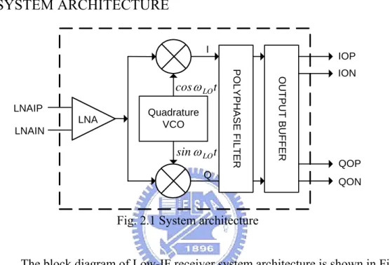
(27) CHPATER 2 CIRCUIT ARCHITECTURE AND SIMULATION RESULTS. CHAPTER 2 CIRCUIT ARCHITECTURE AND SIMULATION RESULTS 2.1 SYSTEM ARCHITECTURE I. LNA LNAIN. Quadrature VCO. sin ω LO t. OUTPUT BUFFER. LNAIP. POLYPHASE FILTER. cos ω LO t. IOP. Q. ION. QOP QON. Fig. 2.1 System architecture The block diagram of Low-IF receiver system architecture is shown in Fig. 2.1. The receiver architecture includes a low noise amplifier, quadrature VCO, quadrature mixer, polyphase filter, and an output buffer in the last stage. LNA provides a high gain but low noise figure to amplify the RF signal. It amplifies the desired signal and suppresses noise interference. LNA also provides a 50Ω input matching for antenna and transmission line. The LNA is the frist stage of receiver system. It plays an important role on noise figure for whole receiver system. The LNA output transfers RF signal to next stage. The quadratuere mixer used to down-converts the RF signal to IF signal. A quadrature VCO generates LO signals with 90-phase difference. As shown in Fig. 2.2, the quadrature LO signal is used to mixes with RF signal to generate IF I/Q signal. 13.
(28) CHPATER 2 CIRCUIT ARCHITECTURE AND SIMULATION RESULTS. The quadrature mixer stage follows the LNA. The quadrature mixer mixes RF signal and quadrature LO signals. The quadrature mixer is used to downconverts RF band to IF band and splits the IF band to I/Q phase difference. The mismatch of VCO and mixer can degrade the image rejection ratio. Polyphase filter and output buffer is a complex filter in the last stage, which follows the RF mixer, used to suppress the image signal and employ a common source buffer to transfer the desired signal in IF band. The desired and image signals can be distinguished in phase relation and double-ended spectrum. The polyphase filter generally can be easily realized by passive R-C polyphase network. The main disadvantage is the signal loose. The receiver in this design used an active polyphase filter to solve the image signal and improve the linearity. The common source output buffer must consider the linearity and used to drive the output load. It provides enough output power to drive the output capacitance and eliminate output loss as far as possible. Layout and design strategies are considered to achieve high performance and image rejection ratio in this architecture. The whole chip floorplan, mismatch, The symmetry of differential circuit, robust power line, and signal transmission line are the key points to eliminate the ill effect in layout.. 2.2 OPERATIONAL PRINCIPLE This section describes the principle of the receiver, it presents how the receiver down-converts RF band signal to IF band signal. It also shows the image cancellation methodology. The typical function of downcoversion is to do a multiplication operation. It assumes the RF signal is e jω RF t and the LO signal is e jω LOt . To multiply these two signal and input to an analog multiplier. Then the mixer generates an IF frequency. 14.
(29) CHPATER 2 CIRCUIT ARCHITECTURE AND SIMULATION RESULTS. ω RF − ω LO . i.e. ω IF = ω RF − ω LO . The following are the mathematical representations with an assumption of ω RF > ω LO , to multiply the RF and LO signal with exponential equation (1). e jω RF t × e − jω LO t → e jω IF t. (1). It is an easy way to expand the equation by Eulers’s formula, exponential function and Euler’s formula act as an important role on the discussion of complex signal. After the Eulers’s formula transformation, the operation of mixer operation can be rewritten as follow.. (cosω RF t + j sin ω RF t ) • (cosω LO t − j sin ω LO t ) =. (cosω RF t • cosω LO t + sin ω RF t • sin ω LO t ) + j (sin ω RF t • cos ω LO t − cos ω RF t • sin ω LO t ). = cos(ω RF − ω LO ) + j sin (ω RF − ω LO )t (2). → cos ω IF t + j sin ω IF t. From the equation (2), Quadrature RF signal is multiplied with quadrature LO signal. The procedure generates quadrature IF signal on the output terminal of I-channel and Q-channel. I-channel corresponds to the real part of complex signal and Q-channel corresponds to the imaginary one. I-channel and Q-channel are always with 90-degree phase difference in an identical frequency. The operation of signal multiplication in frequency domain depicts on Fig. 2.2. The equation (1) and (2) can be described and signify in block function diagram, which is shown in Fig. 2.3.. 0. ωRF. ω X. ω. −ωLO 0. Fig. 2.2 Operation of downconversion. 15. 0 ωIF. ω.
(30) CHPATER 2 CIRCUIT ARCHITECTURE AND SIMULATION RESULTS. I. 90o. RF. LO. Q Fig. 2.3 IF quadrature I/Q signal generator. It presented how the equation (2) to be implemented in frequency domain. The quadrature VCO applies I/Q quadrature LO signal with 90-degree phase difference and multiplied with RF input signal. The LO quadrature signal can be denoted to cosω LO t and sin ω LO t . The operation of Low-IF block diagram is shown in Fig. 2.4.. I. cos ω LO t LNAIP. Quadrature VCO. LNA LNAIN. sin ω LO t Q Fig. 2.4 Low-IF quadrature downconverter. 16.
(31) CHPATER 2 CIRCUIT ARCHITECTURE AND SIMULATION RESULTS. Image-reject process. If there exist an image signal e jω IM t , the image frequency has the same frequency. After down-conversion processing, it can be denoted by. ω IF = ω RF − ω LO and ω IF = ω LO − ω IM separately, where the ω IM is the image frequency. The below mathematical equation representations the image signal mixes the LO signal with an assumption of ω IM < ω LO , e jω IM t × e − jω LO t → e − jω IF t. (3). By Euler’s formula, the down-conversion procedure can be rewritten as.. (cosω IM t + = +. j sin ω IM t ) • (cos ω LOt − j sin ω LOt ). (cosω IM t • cosω LOt + sin ω IM t • sin ω LOt ) j (sin ω IM t • cos ω LOt − cos ω IM t • sin ω LOt ). = cos(ω IM − ω LO ) + j sin (ω IM − ω LO )t (4). → cos ω IF t − j sin ω IF t. The signal mixing procedure generates quadrature IF signal on the output terminal of I-channel and Q-channel. The output IF frequency is ω IF . The frequency is similar to ω RF signal mixes with LO signal, which is represented in previous equation (2). Image IF signal contains negative sine function on Qchannel. It should be known that a quadrature image rejection filter must distinguish the desired signal ω RF and undesired image signal ω IM by complex filter. The polyphase filter is usually implement to act as the complex filter to reject the image signal.. 17.
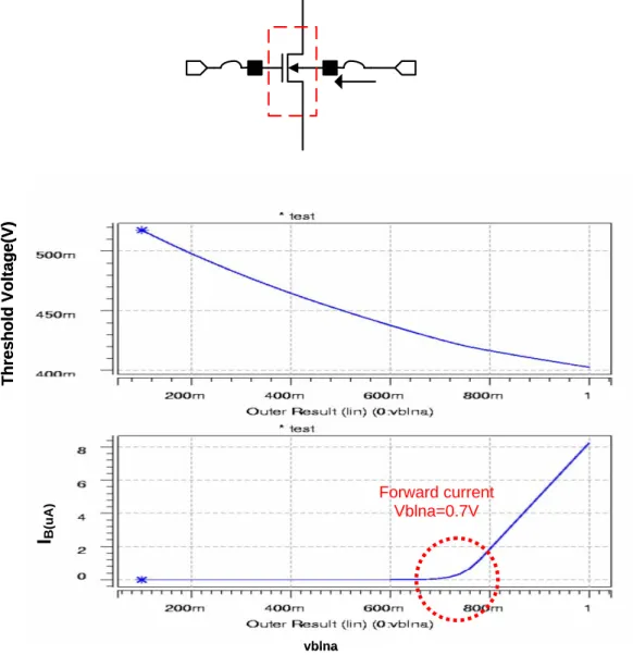
(32) CHPATER 2 CIRCUIT ARCHITECTURE AND SIMULATION RESULTS. 2.3 CIRCUIT DESIGN 2.3.1 Body-biased low noise amplifier (LNA) Low noise amplifier (LNA) is the first stage of the receiver system. The architecture of LNA proposed in this thesis is inductive source degeneration with body-bias scheme. In order to operate at 1-V power supply, the body-bias is applied in cascode input stage. The body-bias is used to improve the voltage headroom, linearity and noise factor. The performance of the LNA is optimized by properly choosing the size of the input and cascade transistors. This strategy can also minimizes noise as possible as for the system. There are several common goals in design of LNA. These include input impedance matching, higher power gain, minimizing the noise figure, sufficient linearity, and small power consumption. Otherwise, it also provides 50Ω input matching for antenna input. A. Body-biased design In order to decrease the threshold voltage of cascade input devices and improve the operation headroom, body-bias voltage is implemented in the LNA design. The body-bias must be supplied in terminal of NMOS bulk that is separated from other NMOS devices. TSMC 0.25um provides an effective method to separate the NMOS substrate that is deep N-well process. The P-well in DEEP NWELL is called RW. It isolates the P-well from other NMOS devices. That not only cancels the NMOS body effect but also the body-bias supplied to the terminal of NMOS bulk independently. The Fig. 2.11 illustrates how the single end cascode NMOS place on deep N-well with body-bias circuit. Fig. 2.5 illustrates the cross section of the LNA input cascade stage. The junction model of MOS device is not. 18.
(33) CHPATER 2 CIRCUIT ARCHITECTURE AND SIMULATION RESULTS. well defined. We must pay attention to the design guard band and sensitive to process variation.. Ld Deep NWELL. MN2. MN1. VBLNA. LNAIN Ls. Fig. 2.5 Single end cascode NMOS place on Deep N-well with body-bias. LNAIP Positive bias VBLNA. P+. N+. N+. P+. N+. N+. P+. N-well. N-well. RW. Deep N-well P-sub. Fig. 2.6 Cross section of cascode NMOS place on deep N-well Shown in Fig. 2.6, it provides a positive body-bias (VBLNA) voltage to the terminal of NMOS bulk. Then a forward parasitic PN junction will be created. It generates a forward current when the body-bias (VBLNA) greater than the PN junction on voltage. A forward current induced into source or drain of the NMOS. This causes the NMOS input stage operation point shift. For this reason, the gain of LNA will be degraded. The top curve of Fig. 2.7 shows the threshold voltage. 19.
(34) CHPATER 2 CIRCUIT ARCHITECTURE AND SIMULATION RESULTS. decrease if VBLNA increase. The bottom curve of Fig. 2.7 shows the IBS forward. Threshold Voltage(V). current is created if the forward VBS voltage VBLNA greater than about 0.7V.. IB(uA). Forward current Vblna=0.7V. vblna. Fig. 2.7 The deviation of threshold voltage and forward current The drain current Id of MOSFET is Id = K (VGS − Vth ) 2 where K and Vth ater the gain factor and the threshold voltage, respectively. In order to obtain a large gain, the current increased. However, the supply voltage is lowered, the drain current is limited. The body of the transistor is connected to the bias voltage. The Vth of the transistor is Vth = Vtho + γ. 20. [. ]. 2φ F − VBS − 2φ F , where Vtho is.
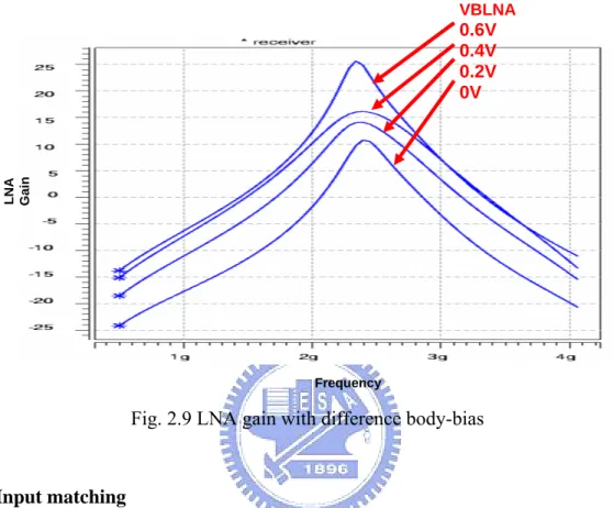
(35) CHPATER 2 CIRCUIT ARCHITECTURE AND SIMULATION RESULTS. the threshold voltage for body-source voltage, VBS=0V, γ is body-effect coefficient, φ F is the bulk potential. As the gate-source voltage (VGS) must be not less than 0V. The threshold voltage becomes smaller due to the body biased effect and this leads to a larger drain current. The transconductance factor (gm) of the body-biased LNA is larger than conventional LNA. The ratio of the gm to gm0, which is the transconductance factor when the body biased at the source, is. (V. GS. gm = gm0. − Vth0 − γ. [. ]). ⎛ 2φ F − VBS − 2φ F ⋅ ⎜1 + ⎜ ⎝ (VGS − Vth0). γ 2φ F − VBS. ⎞ ⎟ ⎟ ⎠. VBLNA=0.6V. LN A G AI N (d B). Too large forward bias. VBLNA (body bias: V). Fig. 2.8 body-bias voltage vs. LNA gain Fig. 2.8 shows the gain of LNA increase if VBLNA increase. The junction forward current destroys the DC operating point of input stage devices and it further decrease the gain of LNA. From the transfer curve of LNA gain with sweep the bias voltage, the best body-bias (VBLNA) is about the range from 0.4V to 0.6V. If The VBLNA greater than 0.6-V will cause the gain of LNA decrease.. 21.
(36) CHPATER 2 CIRCUIT ARCHITECTURE AND SIMULATION RESULTS. Fig. 2.9 illustrates the frequency response of LNA with difference body-bias voltage.. VBLNA. LNA Gain. 0.6V 0.4V 0.2V 0V. Frequency. Fig. 2.9 LNA gain with difference body-bias. B. Input matching There are four kinds of common architectures used in input matching of LNA. Fig.2.2 illustrates four kinds of input matching circuit. They are resistive termination, 1/gm termination, shunt-series feedback and inductive degeneration. Illustrate in Fig. 2.10(a), The resistance termination shunt with input port to provide a 50Ω resistance. The use of real resistor has a poor noise figure. The resistor in this fashion has a deleterious effect on LNA’s noise figure. A second The NF of 1/gm termination is usually larger than 3dB. Shunt-series feedback needs on-chip resistors of reasonable quality. It also often has higher power to provide high gain. The shunt-series feedback approach is not suitable for this work. The inductive degeneration usually has best quality and small noise in this LNA design. 22.
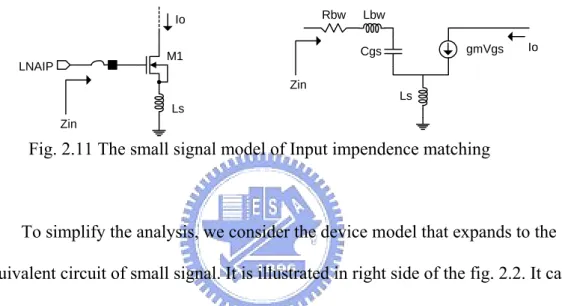
(37) CHPATER 2 CIRCUIT ARCHITECTURE AND SIMULATION RESULTS. Zin Zin. Zin (b). (a). Zin (e). (d). Fig. 2.10 (a) Resistive termination (b) 1/gm termination (c) shunt-series feedback (d) inductive degeneration Fig. 2.11 is the input stage equivalent circuit of source degeneration cascode low noise amplifier. Rbw. Io. gmVgs. Cgs. M1. LNAIP. Lbw. Zin. Io. Ls. Ls Zin. Fig. 2.11 The small signal model of Input impendence matching. To simplify the analysis, we consider the device model that expands to the equivalent circuit of small signal. It is illustrated in right side of the fig. 2.2. It can be show that the input impedance of the circuit is shown as follow:. Zin( s ) =. Vs sCgs ( RG + sLg ) ⋅ Vgs + ( gmVgs + sCgsVgs ) ⋅ sLs = Is sCgsVgs. = RG + sLg +. ⎛ gm ⎞ 1 ⎟ ⋅ Ls + sLs + ⎜⎜ sCgs ⎝ Cgs ⎟⎠. = s ( Lg + Ls ) +. ⎛ gm ⎞ 1 ⎟ ⋅ Ls + RG + ⎜⎜ sCgs ⎝ Cgs ⎟⎠. (5). At the resonate frequency, that is Zin(i)=0 then. s ( Lg + Ls ) +. 1 =0 sCgs. 23. (6).
(38) CHPATER 2 CIRCUIT ARCHITECTURE AND SIMULATION RESULTS. Alternately,. ω o = 2πf o =. 1 ( Ls + Lg )Cgs. (7). From this equation, to evaluate can get the Lg value. in the real part of Zin, Zin(r)=50Ω ⎛ gm ⎞ ⎟⎟ ⋅ Ls = ω t Ls = 50Ω Zin = ⎜⎜ ⎝ Cgs ⎠. (8). Ls value can be evaluated from this equation. Replace the gm/Cgs with mos cut-off frequency, i.e. ft =. gm Cgs. Cgs = K ′ ⋅ W. (9). From this equation, we can see the Zin=50 are related to the mos cut-off frequency. The parasitic of a output pad and bond-wire loading are modeled by a resistance series an inductor and parallel a PAD capacitance; the PAD capacitance is connected to substrate. This model is illustrated in Fig. 2.12. The bond-wire impendence also compensates the input impedance to fit the 50Ω matching. After adjust the bond-wire inductance and capacitance, The low-noise amplifier has best S11 performance.. 24.
(39) CHPATER 2 CIRCUIT ARCHITECTURE AND SIMULATION RESULTS. Rbw. Lbw. =. Cpad. Subtrate Fig. 2.12 Parasitic circuit model of a pad capacitance and bond-wire. C. Voltage gain and linearity For LNA design, Linearity and gain are usually tradeoffs in general condition. The gain generally designed in appropriate range of 15~20dB in a conventional LNA for wireless communication. Fig 2.13 shows the model of LNA small signal analysis equivalent circuit. Rg. Lg gmVgs. Cgs. Io. Ls. Fig. 2.13 LNA Gmeff small signal analysis equivalent circuit. io = gm ⋅ Vgs Ve = ( sCgsVgs + gmVgs) ⋅ sLs Vin = sCgsVgs ( Rs + sLg +. 1 ) + sLs (Vgs ⋅ sCgs + gmVgs) sCgs. [. ]. = Vgs s 2 Cgs ( Ls + Lg ) + s (CgsRs + gmLs ) + 1 Gmeff =. io gm = 2 Vs s Cgs ( Ls + Lg ) + s (CgsRs + gmLs) + 1. 25. (10).
(40) CHPATER 2 CIRCUIT ARCHITECTURE AND SIMULATION RESULTS. At the resonate frequency, we can get the effect transconductance in equ. (11) 1 Cgs ( Ls + Lg ). ωo =. Gmeff =. gm = ω (CgsRs + gmLs ). ωt ⎛ ⎝. ωRs⎜1 +. ω t Ls ⎞ ⎟ Rs ⎠. =. ωt 2ωRs. (11). D. Noise Optimization.. This subsection describes noise performance on the inductor-degeneration configuration and designing an optimal dimension of the MOS devices for minimal noise contribution. Noise figure is an important specification in LNA design. In the cascade network of multi-stage, first stage plays an important role to reduce the total noise figure of the receiver system. The LNA is the first stage of the receiver system. In general, LNA noise figure determine the receiver sensitivity.. Vg 2. C gd. Rg +. C gs. Vgs. gmVgs. id 2. -. ro. Fig. 2.14 small signal noise model of MOS device Fig. 2.14 shows a small signal noise model of the input stage, Rg is gate resistance and Rs is voltage source resistance; Rg can be minimized by good layout. Where Vg 2 and id 2 are induced by Rs and channel resistance respectively. Thermal noise and gate current noise are main source in LNA design. Especially the channel thermal noise is dominant. The equation id 2 is listed in (9). id 2 = 4kTBγg d 0. 26. (12).
(41) CHPATER 2 CIRCUIT ARCHITECTURE AND SIMULATION RESULTS. +. ig 2. Vgs. gg. C gs. -. Fig. 2.15 Equivalent gate circuit A equivalent gate circuit model is shown in Fig.2.15. A shunt noise current ig 2 and a shunt conductance g g have been added. At resonance frequency, the. small signal revised noise model is shown in Fig. 2.16.. Lbw. Rbw. Vg 2. Rg +. Rs. ig 2. gg. Cgs. id 2. gmVgs. Vgs. -. Vs 2. iout. 2. Ls. Fig. 2.16 Revised Noise model 2 2 Rbw Rg γg d 0 Rsω C gs F = 1+ + + Rs Rs g m2. Rg ⎛ω R F = 1 + bw + + γg d 0 Rs ⎜⎜ Rs Rs ⎝ ωT. ⎞ ⎟⎟ ⎠. (13). 2. (14). A common form of the noise factor is listed in equ. (13). It is re-arranged to equ. (14). It is observed that It can further decrease noise factor by to reduce g d 0 . To achieve low noise factor involves linearity tradeoff. Besides, the technology scaling is a key.. Rg ⎛ω R + γg d 0 Rs ⎜⎜ F = 1 + bw + Rs Rs ⎝ ωT. ⎞ ⎟⎟ ⎠. 2. ⎧⎪ δα 2 δα 2 + + 1 2 Q c 1 + QL2 ⎨ L 5 5 γ γ ⎪⎩. [. 27. ⎫. ]⎪⎬ ⎪⎭. (15).
(42) CHPATER 2 CIRCUIT ARCHITECTURE AND SIMULATION RESULTS. E. Low-Noise Amplifier Circuit Implementation. The new LNA with body-bias circuit is proposed in this thesis. The LNA uses common-source degeneration cascode with fully differential configuration. Shown in Fig. 2.17, its device size is listed in table I. MN1, MN2 provide the enough gain and noise optimization. MN1, MN2, LS1 and LS2 are designed to optimize the input matching. MN3, MN4 isolate the input RF signal input and LNA output. LD1, LD2 and CC1, CC2 provides impedance for voltage gain in resonate frequency. The body-bias is applied for MN1, MN2, MN3 and MN4. For this reason, these devices are placed in a deep-NWELL structure to isolate with other NMOS P-substrate. The body-bias scheme can further decrease the threshold voltage and improve the gain and linearity. All inductors are spiral inductor supplied by TSMC 0.25-um technology. A sub-circuit in HSPICE simulation models the behavior of inductor, MIM capacitance.. 28.
(43) CHPATER 2 CIRCUIT ARCHITECTURE AND SIMULATION RESULTS. Fig. 2.17 LNA circuit. Device Name MN1,MN2 MN3,MN4 XLS1,XLS2 XLD1,XLD2 CC1,CC2. W/L(um/um) 120/0.24 10/0.24 2.5n 4.7n 0.1p. Table 2.1 LNA device parameter. 29.
(44) CHPATER 2 CIRCUIT ARCHITECTURE AND SIMULATION RESULTS. 2.3.2 Quadrature voltage control oscillator This receiver involves the design of circuit to generate a quadrature LO signal with 90-phase difference. The most popular method is to use a voltagecontrolled oscillator (VCO), which is usually in the form of the LC-tank. High frequency oscillator usually comprises a resonator, which includes inductor, capacitor, and negative resistor. Fig. 2.18 illustrates the standard circuit of typical resonator. In order to generate quadrature LO signal, a structure of VCO based on even-stage ring oscillator usually be used.. -R. L. C. Fig. 2.18 Typical RLC tank Fig. 2.9 is the conceptual block diagram of the quadrature VCO. This structure is like as a two-stage ring oscillator. INV1 and INV2 are identical fully differential inverter. The ring oscillator was combined with two fully differential inverters. Finally, The inverters connect to LC-tank load and a negative resistor respectively. Fig. 2.19 further depicts the fully differential inverter with LC-tank and negative resistor. MN5 and MN6 act as the negative resistor to cancel the parasitic resistor. Two spiral inductor and varactor decide the frequency of oscillator. MN1 and MN2 act as fully differential inverter. The inverter output terminal is VO1 and VO2. Two identical inverters are combined together for two-stage ring-oscillator. To observe the output DC level can bias at VDD.. 30.
(45) CHPATER 2 CIRCUIT ARCHITECTURE AND SIMULATION RESULTS. -R1. -R2. L1. L2. LOIP LOIN. C1. C2. - +. - +. + -. + -. LOQP LOQN. INV2. INV1. Fig. 2.19 Conceptual block diagram of the quadrature VCO The fully circuit of quadrature voltage-controlled oscillator in this thesis is shown in Fig. 2.21. The output terminal of VCO connected to next stage(mixer) directly.. VO1. VO2. VCOVB. N1 V1 N5. N2. V2. N6. Fig. 2.20 Fully differential inverter with LC-tuned in the quadrature VCO. 31.
(46) CHPATER 2 CIRCUIT ARCHITECTURE AND SIMULATION RESULTS. XL1. XL4. XL2 XL3 XC1. LOIN. XC2. XC3. LOIP LOQN. XC4. LOQP. VCOVB VCOVB. N=8 MN5. N=8. MN1. MN2. N=8. MN3 MN4. MN6. N=8. MN7. Fig. 2.21 The whole circuit of quadeature voltage-controlled oscillator circuit. Device Name MN1,MN2,MN3,MN4 MN5,MN6,MN7,MN8 XL1,XL2,XL3,XL4 XLD1,XLD2 XC1,XC2,XC3,XC4. W/L(um/um) 10/0.36 40/0.24 2.5n 1.05n 0.049p. Table 2.2 QVCO device parameter. 32. MN8.
(47) CHPATER 2 CIRCUIT ARCHITECTURE AND SIMULATION RESULTS. 2.3.3 Quadrature mixer This section discussed the principle and design methodology of the downconverter mixer. Consider the Fig. 2.22, refer the drain current of basic unit PMOS cell. By means of the PMOS drain current operating equation in saturation, the mixer can achieve the mixing operation. PMOS is a basic unit cell in this mixer design. First, we can observe that the PMOS current is the function of gate to drain voltage in saturation region.. (16). I d = K (Vgs − Vt ) 2 Where the constant K is K=. (17). 1 ⎛W ⎞ µ n Cox ⎜ ⎟ 2 ⎝L⎠. In order to simplify the following analysis and to make it clearly, replace the gate and drain terminal to ‘Va’ and ‘Vb’ respectively. The drain current of the PMOS device can be written as. I d = K (Vgs − Vt ) 2 = K [(Va 2 − 2Va ⋅ Vb + Vb 2 − 2(Va − Vb ) ⋅ Vt + Vt 2 ]. (18). Thus, the voltage of Vmx1 shown in Fig. 2.22 will become (Vt is replaced by constant value C ) Vmx1 = I d × Z L = KZ L [(Va 2 − 2Va ⋅Vb + Vb 2 − 2(Va − Vb ) ⋅ C1 + C 2 ]. Va Vb Vmx1 Id. ZL. Fig. 2.22 Basic PMOS unit cell of mixer. 33. (19).
(48) CHPATER 2 CIRCUIT ARCHITECTURE AND SIMULATION RESULTS. Va. -Va. Vb. -Vb Vmxp ZL. Id. Fig. 2.23 Mix Va and Vb operation constructed by two basic PMOS device Illustrate in Fig. 2.23, merge two basic PMOS unit cells as and summation the Id current flow through the Z L . The Id current can be deriving as. I d = K [(Va 2 − 2Va ⋅Vb + Vb 2 − 2(Va − Vb ) ⋅ C1 + C 2 ]. (20). + K [(Va 2 − 2Va ⋅Vb + Vb 2 − 2(− Va + Vb ) ⋅ C1 + C 2 ]. = 2(Va 2 + Vb 2 ) − 4Va ⋅ Vb + 2C 2 (21). Vmx 2 = I d × Z L = [2(Va 2 + Vb 2 ) − 4Va ⋅ Vb + 2C 2 ]Z L. Va. Va. -Va. Vb. -Va. -Vb Vmxp Id. ZL. Vb Vmxn ZL. Id. Fig. 2.24 double-balanced mixer structure The Fig. 2.24 shows the double-balanced mixer structure. Vmxp − Vmxn = [2(Va 2 + Vb 2 ) − 4Va ⋅Vb + 2C ] ⋅ Z L. (22). − [2(Va 2 + Vb 2 ) + 4Va ⋅Vb + 2C ] ⋅ Z L = 8 ⋅Va ⋅Vb To replace the sign of equations. It can be Va=LOIP, -Va=LOIN, Vb=MXIP, -Vb=MXIN. 34.
(49) CHPATER 2 CIRCUIT ARCHITECTURE AND SIMULATION RESULTS. LOIP. LOIN. LOQP. LOQN. VBMXRF 1k. 1k. MP1. MP3. MP2. MP4. MP5. MP7. MP6. MP8. MXIP MXIN. MXIP MXIN. MXIP. MXIN. XC4. XC2 IFIP. IFQN XC1. IFIN. XC3. IFQP. VBMXIF MN1. MN2. MN3. MN4. MN5. Fig. 2.25 Quadrature downconversion mixer schematic. Device Name MP1,MP2,MP3,MP4, MP5,MP6,MP7,MP8 MN1,MN2,MN3,MN4 XC1,XC2,XC3,XC4. W/L(um/um) 5/0.3 10/0.24 0.9p. Table 2.3 Mixer device parameter. 2.3.4 Active polyphase filter The polyphase filter and output buffer are the last stage of receiver front-end system. The polyphase filter stage that follows the mixer and selected the desired signal to output. The polyphase filter is used to reject image interference in a receiver front-end system. It must have the features with high image rejection ratio, low sensitivity to mismatching components, sufficient linearity, and low power consumption in the design of integrated RF front-end receiver. When the input signal is clockwise or positive frequency, the RF signal down converted IF signal passes to output. Contrary, the signal is anti-clockwise or negative frequency; the. 35.
(50) CHPATER 2 CIRCUIT ARCHITECTURE AND SIMULATION RESULTS. filter should reject the image IF signal. In the application of monolithic integration, the polyphase filter design must be easily integrated in a receiver chip. The polyphase filter is a complex filter; most of popular of polyphase filter is RC sequence network. It is comprise of two passive components, which are resistor and capacitance to do the filter operation. The center frequency of onestage RC polyphase filter can be determined by ω = 1 / RC for narrow band design. The amplitude of the output will be equal only at the input frequency. The transfer function of RC network depends on phase order of the input sequence. In order to prevent process variation and increase variation guard band, a multi-stage RC network can be used to achieve a broadband design. M-stage network can be constructed by cascading M-stage to expand the bandwidth of the filter. The 4stage RC polyphase filter network is shown in fig. 2.26.. Fig. 2.26 4-stages RC network polyphase filter The main disadvantage of the multi-stage RC polyphase filter is its signal loose. This will cause received signal decay and decrease the noise figure (NF) performance of the receiver system. In this thesis, we use an active polyphase filter for the Low-IF receiver application. The advantages of the active polyphase filter are its high input impendence in each stage and provide enough gain to amplify the IF desired signal. It prevent the degradation of the gain lose. Besides, it eliminates the extra. 36.
(51) CHPATER 2 CIRCUIT ARCHITECTURE AND SIMULATION RESULTS. power dissipation. Simultaneously, the high gain is assigned to the first stage to improve the better noise performance. The main consideration of polyphase filter is its image rejection ratio (IRR), tolerance in process variation, bandwidth, linearity and power consumption. As the transfer function of complex filter, this is similar to RC network polyphase filter to perform the positive or negative frequency filter. The filter must distinguish positive frequency and negative frequency. In the point of view in filter transfer function, it is combination of 1st order low-pass and high pass transfer function. The transfer function of a complex filter can be represented as. H (ω ) = H 1 (ω ) + jH 2 (ω ). (23). Where H 1 (ω ) and H 2 (ω ) are real transfer function. If a complex signal. I (ω ) + jQ(ω ) is applied to this complex filter, the output signal R(ω ) can be rewritten as R (ω ) = I (ω ) H 1 (ω ) − Q (ω ) H 2 (ω ) + j ( I (ω ) H 2 (ω ) + Q (ω ) H 1 (ω )). (24). The block diagram of simple complex filter was presented in Fig. 2.27. I ( ω ) + jQ( ω ). H 1 ( ω ) + jH 2 ( ω ). I ( ω )H 1( ω ) − Q( ω )H 2 ( ω ) + j( I ( ω )H 2 ( ω ) + Q( ω )H 1( ω )). Fig. 2.27 The principle of complex filter To expand the equation to first order high pass and low pass filter with single pole. The transfer function H ( s ) can be represented as follow. ⎛ 1 s H ( s ) = H 1 ( s ) + jH 2 ( s ) = A ⋅ ⎜ + ⎜s + ω s +ωp p ⎝. 37. ⎞ ⎟ ⎟ ⎠. (25).
(52) CHPATER 2 CIRCUIT ARCHITECTURE AND SIMULATION RESULTS. Where A is the gain of the transfer function and ω p is the position of single pole. H 1 ( s ) and H 2 ( s ) are the first order low pass and high pass equation. The image signal can be rejected by this equation at the frequency ω p . A 1-stage polyphase filter can be implemented by combination of first order low-pass and high-pass filter circuit. Ii(ω). H 1(ω). Io(ω)=I(ω)H 1(ω)-Q(ω)H 2(ω). -. H 2(ω). H 2(ω). + +. H1(ω). Q i(ω). +. +. +. Qo(ω)=I(ω)H 2(ω)+Q(ω)H 1(ω). Fig. 2.28 Using real filter realize complex filter In order to increase the tolerance of process variation, the bandwidth of filter must be expanded. Wide bandwidth can be achieved by cascade multi-stage. LP1. +. LP2. +. LP3. +. LP4. HP1. HP2. HP3. HP4. HP1. HP2. HP3. HP4. LP1. -. LP2. -. LP3. -. +. LP4. -. Fig. 2.29 The four-stage polyphase filter This design implements a four-stage polyphase filter to expand the bandwidth and enhance the tolerances of process variation. Fig. 2.29 illustrates the four-stage polyphase filter design in this chip. The poles of each stage are difference to fine-tune the bandwidth and operating frequency. The poles are determined by changing CH for each one-stage polyphase filter. The polyphase filter also provides enough gain to amplify the IF signal and prevent the best performance of linearity.. 38.
(53) CHPATER 2 CIRCUIT ARCHITECTURE AND SIMULATION RESULTS. fp =. 1 1 = = 2.76MHz 2πRC 2π ⋅ 3.6k ⋅ 3.6 p. Fig. 2.30 Polyphase filter input bias.. Fig. 2.31 1-stage polyphase filter. Fig. 2.32 4-stage polyphase filter. 39.
(54) CHPATER 2 CIRCUIT ARCHITECTURE AND SIMULATION RESULTS. Fig. 2.33 output buffer Type Passive Polyphase filter 1 Decided by RC. Active Polyphase filter Decided by gm and C pole HP: gm r ⋅α ⋅ gm1 ⋅ ( 1 ) Vol Ch = gm1 Vp s+( ) Ch LP: Voh r ⋅ α ⋅ gm1 ⋅ s = gm Vp s+( 1) Ch (W/L)mp3=(W/L)mp4= α (W/L)mp1 Device RC MOS, C Area Large area Small area Input impedance Low input impedance High input impedance Gain Lossy Provide gain Extra amplifier Additional buffer no need of extra amplifier Power More power for buffer Smaller than passive filter Table 2.4 Compare with passive and active polyphase filter.. The mirrored current I3 is then divided into IL and IH by a diode-connected transistor MI, and a capacitor, CH, respectively. IL and IH can be derived as.. Vol = Vp. r ⋅α ⋅ gm1 ⋅ (. gm1 ) Ch. gm s+( 1) Ch. 40. (26).
(55) CHPATER 2 CIRCUIT ARCHITECTURE AND SIMULATION RESULTS. Voh r ⋅ α ⋅ gm1 ⋅ s = gm Vp s+( 1) Ch. (27). Where α is the value of (W/L)3/(W/L)1, and gml and gmh are the transcoductances of Ml and ML, respectively. (W/L)mp3=(W/L)mp4= α (W/L)mp1 The bias voltage of each stage must adjust to gain a best performance of receiver. It is observed the positive frequency gain loss in lower frequency. It is because of the input stage HP filter. It is shown in Fig.2.30. The pole of the HP filter is about 2.76MHz. Lower pole frequency is best but it is trade-off between area and low pole. The Fig. 2.31 presents the circuit of 1-stage polyphase filter. Fig. 2.32 presents the circuit of 4-stage polyphase filter. The output buffer is shown in Fig.2.33. Table 2.4 shows the comparison between passive and active polyphase filter. The main disadvantage of the multi-stage passive polyphse filter is that it is lossy, and thus received signal decays and the overall noise figure (NF) of the receiver is degraded. Additional buffer should be inserted among stage to overcome this drawback. However, additional buffer means it consumes extra power. Furthermore, a larger area is required to implementation numbers of passive resistors and capacitors in the RC polyphase filter.. 41.
(56) CHPATER 2 CIRCUIT ARCHITECTURE AND SIMULATION RESULTS. 2.4 RECEIVER REALIZATION The designed receiver has been implemented on a single testchip; it comprises a body-biased LNA, a quadrature VCO, a quadrature mixer, polyphase filter and an output buffer. 1-V power supply design is a challenge on TSMC 0.25-um technology in many conventional circuit structure. The body bias VBLNA for LNA to gain the headroom of LNA. All inductors employed are spiral inductors made of top thick metal; varactors are N-well structure; resistors are polysilicon with P-type implant. To avoid the body-effect, all N-mos device contain deep N-well for equal voltage between VBS. The model including spiral inductor, MIM capacitor, varactor and deep NWELL NMOS devices is supported by TSMC. The design is checked by LPE parasitic RC extraction based on TSMC’s spice model document to evaluate the simulation results. In order To avoid body effect of NMOS, all NMOS devices contain deep NWELL to make VSB voltage is zero. All spiral inductors made of top thick metal; Varactors are N-WELL structure; resistors are made of polysilicon with p-type implant. The buffer circuit as output stage follows the polyphase filter for measurement. The circuit comprises four common-source stage, following the four terminals of the polyphase filter respectively. The Fig.2.30 in next page presents the complete schematic of proposed Low-IF receiver.. 42.
(57) CHPATER 2 CIRCUIT ARCHITECTURE AND SIMULATION RESULTS. VCOVB. MN5. LOIP. N=8. XL1. LOIP. MN6. MN1. MP1. 1k. MP3 MP2. MXIN. XC2. XC1. LOIN. MN2. XC2. XC1. QVCO. N=8. 1k. MXIP. IFIP. MN2. MP5. LOQP. XL2 XL3. LOIN. MP4. XLS2. XC3. XC4. MN3 MN4. LOQP. MP6. XL4. LOQN. N=8. LOQN. VCOVB. MXIN. IFQN. LNAIN. MN5. MP8. MN7. 0.2p 12.4N. LNAOP. XC3. XC4. MXIP. MP7. MN4. MN2. MN4. XLD2. IFQP. MXIP MXIN. IFIN. MN3. CC1. CC2. VBLNAI. XLD1. MN3. MN1. NVSS. N=8 MN8. MN5. MN5. MN5. MN5. ION. QON. QON. ION. ION. QON. QON ION. XC3. MN4. XC3. MN4. XC3. MN4. XC3. MN4. MP3. VP. MP1. MP1. MN3 MN1. MP3. VP. MP1. MN3 MN1. MP3. VP. MP1. MN3 MN1. MP3. XC1. XC1. XC1. MP2. MP5. VN. MP5. MN2 MN6. MP2. VN. MP5. MN2 MN6. MP2. VN. MP5. MN2 MN6. MP2. VN. MN2 MN6. MP6. MP6. MP6. MP6. XC4. MN7. XC4. MN7. XC4. MN7. XC4. MN7. ION. ION. QON. ION. QON. ION. QON. QON. MN5. MN5. MN5. MN5. IOP. MN8. MN8. MN8. QOP. IOP. QOP. IOP. QOP. IOP. QOP. MN8. XC3. MN4. XC3. MN4. XC3. MN4. XC3. MN4. MP4. MP4. MP4. MP4. MP3. VP. MP1. MP1. MN3 MN1. MP3. VP. MP1. MN3 MN1. MP3. VP. MP1. MN3 MN1. MP3. VP. MN3 MN1. XC1. XC1. XC1. MP5. VN. MP5. VN. MP5. VN. MP5. VN. MN2 MN6. MP2. MN2 MN6. MP2. MN2 MN6. MP2. MN2 MN6. MP2. MP6. MP6. MP6. MP6. 4-STAGE POLYPHASE FILTER MP4. MP4. MP4. MP4. VP. MN3 MN1. XC1. XC4. MN7. XC4. MN7. XC4. MN7. XC4. MN7. IOP. QOP. IOP. QOP. IOP. QOP. IOP. QOP. MN8. MN8. MN8. MN8. MN1. R1. MN2. R2. MN3. MN4. R3. R4. OUT4. OUT3. OUT2. OUT1. BUFFER. IN1. IN2. IN4. IN3. 43. MIXER VBMXRF. MN1. VBMXIF. NVSS. 12.4N 0.2p. LNAON. LNA. LNAIP VBLNA. XLS1. XC1. Fig. 2.34 whole chip of receiver schematic.
(58) CHPATER 2 CIRCUIT ARCHITECTURE AND SIMULATION RESULTS. 2.5 SIMULATION RESULT The receiver chip is simulated by HSPICE. Post-simulation is completed by HSPICE with spice model of TSMC .25-um 1P5M process. This section presents the post-simulation results of all circuit constructing the receiver. A. Low noise amplifier. LNA is the first stage of the receiver; it provides input matching, voltage gain and low noise contribution for the receiver. Fig. 2.31 and Fig. 2.32 show the simulated input matching (S11) lower than –20dB and voltage gain higher than. Gain (dB). 20dB, respectively.. FF FS TT SF SS. Frequency (Herz) Fig. 2.35 simulated voltage gain of the LNA. This fig.2.35 shows the dependence of gain due to process variation. The gain is about 12dB in worst case SS corner simulation. The gain of LNA can guarantee at least larger than 10dB for five corner simulation and meet the specification.. 44.
(59) CHPATER 2 CIRCUIT ARCHITECTURE AND SIMULATION RESULTS. Fig. 2.36 The simulated input matching (S11) of the receiver The Fig.2.36 shows the body bias sweep from 0.3V to 0.6V, the input matching (S11) of LNA can guarantee smaller than -12-dB. body bias and linearity. Ideal curve -6. -10dBm. P a v s (d B ). linearity (dBm). -7 -8 -9 -10 -11 -12 -13 -14. -48. -46. -44. -40. -42. 0. 0.1. 0.2. PL (dB). 0.3. 0.4. 0.5. body bias (V). P1dB@VBLNA=0.5V. (a) -5.5dBm. Pout (dBm ). -2. -4. -6. -13. -11. -9. -7. -5. Pin(dBm). (b) Fig. 2.37 (a) LNA P-1dB HSPICE simulation result. (b) redesign the LNA gain to 6dB, P-1dB can be improved to -5.5dBm. 45. 0.6.
(60) CHPATER 2 CIRCUIT ARCHITECTURE AND SIMULATION RESULTS. Fig. 2.38 LNA noise figure SpectreRF simulation [email protected]. This work Reference paper Simulation results Experimental results with body bias w/o bulk bias Active body Body effect (same device size*) type LNA[11] feedback[14] Technology 0.25um bulk 0.25um bulk 0.35um SOI 0.18 bulk Frequency 2.4GHz 2.4GHz 1.9GHz 1.65~2.5GHz Bulk voltage 0.5V VBS=0V 0.5V 0.6V Supply Voltage 1V 1V 1V 0.9V Power 3.17mA 3.5mA 5mA 2.5mA Consumption S11 -20dB -20dB Gain 20.2dB 16dB 7dB 10dB NF 2.02dB 3dB 5.6dB 1.34dB P-1dB -10dBm -13dBm -4.5dBm -16dBm Table 2.5 The comparison between w/o body bias, w/i body bias.and reference paper The comparison between w/o body bias, w/i body bias.and reference paper is listed in table 2.5. The main advantages of body biased LNA are gain and linearity for low power supply design [11]. 1. Gain improvement 2. 1-dB compression point improvement. 46.
(61) CHPATER 2 CIRCUIT ARCHITECTURE AND SIMULATION RESULTS. The body of the transistor is connected to its gate. The threshold voltage of the transistor becomes smaller due to body effect so that a large drain current is obtained which keeps the gain high even at a low supply voltage. An added feature of connection between the body and the gate is the high 1-dB compression point. This is because the transistor can drive large load capacitance with a larger RFsignal input due to the active threshold voltage of the body control. B. Quadrature Voltage control oscillator. The tuning range of VCO is shown in Fig. 2.33. The quadrature VCO oscillates 2376MHz~2639MHz by control voltage (VCOBIAS) from 0V to 1V. Fig. 2.39 The simulated tuning range of VCO. 47.
數據
+7


相關文件
To complete the “plumbing” of associating our vertex data with variables in our shader programs, you need to tell WebGL where in our buffer object to find the vertex data, and
In the school opening ceremony, the principal announces that she, Miss Shen, t is going to retire early.. There will be a new teacher from
首先,在前言對於為什麼要進行此項研究,動機為何?製程的選擇是基於
The peak detector and loop filter form a feedback circuit that monitors the peak amplitude, A out, of the output signal V out and adjusts the VGA gain until the measured
Students are asked to collect information (including materials from books, pamphlet from Environmental Protection Department...etc.) of the possible effects of pollution on our
接收器: 目前敲擊回音法所採用的接收 器為一種寬頻的位移接收器 其與物體表
Corollary 13.3. For, if C is simple and lies in D, the function f is analytic at each point interior to and on C; so we apply the Cauchy-Goursat theorem directly. On the other hand,
Corollary 13.3. For, if C is simple and lies in D, the function f is analytic at each point interior to and on C; so we apply the Cauchy-Goursat theorem directly. On the other hand,
