國 立 交 通 大 學
電 子 物 理 系 碩 士 班
碩 士 論 文
氟氮離子摻雜應用於金屬閘極與高介電常數絕緣層之
低溫多晶矽薄膜電晶體
Impact of Fluorine and Nitrogen Implantation on
LTPS TFTs with Metal Gate and High-k Dielectric
研 究 生:楊 宗 諭
氟氮離子摻雜應用於金屬閘極與高介電常數絕緣層之
低溫多晶矽薄膜電晶體
Impact of Fluorine and Nitrogen Implantation on
LTPS TFTs with Metal Gate and High-k Dielectric
研究生 :楊宗諭 Student:Tsung-Yu Yang
指導教授:趙天生 博士 Advisor:Dr. Tien-Sheng Chao
國 立 交 通 大 學
電 子 物 理 系 碩 士 班
碩 士 論 文
A Thesis
Submitted to Department of Electrophysics
College of Science
National Chiao Tung University
in partial Fulfillment of the Requirements
for the Degree of
Master
in
Physics
June 2007
Hsinchu, Taiwan, Republic of China
氟氮離子摻雜應用於金屬閘極與高介電常數絕緣層之
低溫多晶矽薄膜電晶體
學生: 楊 宗 諭 指導教授: 趙 天 生 博士
國 立 交 通 大 學
電 子 物 理 系 碩 士 班
摘 要
在本論文中,我們利用低溫製程(< 600o C ),在多晶矽中使用離子佈植引入 氟(fluorine),氮(nitrogen)離子,控制其濃度與能量的離子佈植,再搭配後閘極製 程,覆蓋高介電常數閘極絕緣層二氧化鉿(HfO2)與金屬閘極,成功的製作具有出 色次臨界擺幅(sub-threshold swing)的低溫多晶矽薄膜電晶體(LTPS TFTs)的元 件。我們首先使用正偏壓溫度不穩定(Positive Bias Temperature Instability)的量測 方法,去找出最佳能量以及劑量的元件,期望在最佳缺陷覆蓋的情況下,與沒有 經過離子佈植的元件做比較。在找出最佳能量與劑量的元件後,我們使用熱載子(Hot Carrier Stress)量測方 法,驗證了氟與氮在汲極端的接面缺陷覆蓋的能力,以及同時也發現了使用電子 槍(e-gun)製作的二氧化鉿,在抵抗熱載子破壞時表現較差,在熱載子方法後的量 測發現有閘極漏電,表示熱載子在二氧化鉿內形成嚴重的缺陷,促使電子有漏電 路徑,而有氟的摻雜的元件閘極漏電較低,由於氟離子擴散進入二氧化鉿修補大 部分缺陷,且同時熱載子也不易打斷有氟離子的鍵結,因此在缺陷捕捉相關的參 數-臨界電壓變動,具有較小的變化量。 在熱載子效應後,接著進行正偏壓溫度不穩定的量測方法,從隨時間變動的 臨界電壓(threshold voltage)以及次臨界擺幅,發現臨界電壓的變動趨勢與臨界擺 幅變動趨勢不符合,表示二氧化鉿的原生缺陷補捉是造成臨界電壓變動的主因, 而臨界擺幅的變動也可得知有氟,氮處理元件具有比較好的介面可靠度。之後, 進行了升溫量測,由升溫後的轉換特性曲線也可以說明氟離子具有較好的汲極端 缺陷控制能力,使得熱電子激發(thermionic emission)產生的漏電流較少,再從升 溫前後的臨界電壓的表現可以得知,由於溫度使得捕捉電子更容易被釋放,因此 推測有摻雜氟的元件其通道以及閘極絕緣層中間的介面氧化層較薄,使得捕捉電 子容易在高溫的情況下逃脫。
Impact of Fluorine and Nitrogen Implantation on
LTPS TFTs with Metal Gate and High-k Dielectric
Student: Tsung-Yu Yang Advisor: Dr. Tien-Sheng Chao
Department of Electrophysics
National Chiao Tung University
Abstract
In this thesis, fluorine and nitrogen ions with different dosage and energy were implanted into polycrystalline silicon of thin film transistor with the gate-last process in all low temperature process < 600oC. After deposition of HfO2 high-k gate
dielectric and metal gate, the Low-Temperature-Poly-Si Thin Film Transistors which have excellent sub-threshold swing were fabricated. In order to find out the best device with proper implant dosage and energy, we use the method of positive bias temperature instability, which could help us to find out the best defect-passivation condition.
After finding out the best implant dosage and energy conditions, hot carrier stress method was used to qualify the fluorine and nitrogen passivation ability in the drain-side junction. It is found that the gate dielectric HfO2 which fabricated by the
e-gun exhibited the worse performance to resist the hot carrier damage. After stress, transferred curves show serious gate leakage, which means hot carriers create damage inside the HfO2, resulting in a path for electron to tunnel through gate dielectric. It is
found that a lower gate leakage current was found in the F-implanted devices, which maybe due the passivation of defects by fluorine. On the other hand, strong Si-F bonds exhibit good resistance to hot carrier, causing less threshold voltage shift which is strongly defect-related.
After hot carrier stress, devices were evaluated by using positive bias temperature instability test. With different trends in the time evolution of threshold voltage shift and sub-threshold swing degradation, it is found that electron trapping in the HfO2 is the major reason for the threshold voltage variation. Compared to control
devices, devices with fluorine and nitrogen exhibit good passivation at the interface. Devices were measured at an elevated temperature. The transferred curves measured at higher temperature show that fluorine implantation reduces the thermionic emission current at the drain junction. Finally, from the shift of the threshold voltage, it is found that the electron trapping in the HfO2 could easily be de-trapped at high temperature.
This can be explained by that interfacial oxide layer between gate dielectric and channel can be suppressed with F-incorporation, so that trapping electrons could
致 謝
兩年,真的很快就過去了,在這個小家庭裡面,很高興跟大家一起度過。 老師趙天生是我最想感謝的第一人。還記的一開始在老師辦公室從不會刻畫 一個個製程,到最後量測結果細心的與我一齊討論;也記的一起到二餐吃飯,大 家在餐桌前,老師跟大家一起開我玩笑:叮嚀我要吃菜、不要吃速食,要多走樓 梯,等等有趣的事情,就像剛剛發生一樣歷歷在目。在這裡最印象深刻的,就是 老師說過「家庭」是最重要的事,或許我還不懂,可是就是覺得這句話很重要; 也許我曾經是個令老師頭痛的學生,但是我在此衷心感謝老師的指導與包容。 再來要感謝馬鳴汶學長,在實驗時的嚴謹態度,量測資料的分析與整理,糾 正許多元件物理上的觀念,這些經驗的傳授,由衷感謝;還要感謝郭伯儀學長在 早期做實驗對我的指導,以及最後仔細耐心的跟我一起分析資料,還有一齊去爬 山、去游泳以及打壘球的回憶,我都會謹記在心的;然後就是感謝搞笑的電物一 哥吳偉成學長,不可否認的待人處世觀念一把罩,還有打球跑步沒多久就要喘半 天,最後在找工作時還幫了大忙,我從你身上真的學到很多;還有感謝起初我以 為很難搞笑的羅文政學長,可是私底下卻常常說各種運動都很強的學長,在最後 整理數據時給我很有用的意見;還要感謝在量測時大力幫忙的陳建豪學長,在分 析數據上的想法很值得我多多學習;以及在報告技巧上指導的呂宗宜學長、常來 實驗室分享東西的吳家豪學長以及曾經一同在期末報告努力的張宗憲學長,非常 感謝你們的分享與指導。 此外,還要感謝已畢業的黃竣祥學長,黃彥學學長,謝佩珊學姊,彭武欽學 長、周棟煥學長、陳煒昕學長,在 NDL 裡面仔細且耐心教導我實驗技巧,以及在 模擬技巧上的傳授。還要感謝跟我一齊度過兩年的同學國興、德鑫、美君、宜憲、 妍心、明宏以及久騰,在做實驗互相幫忙、Meeting 與演講睡過頭幫忙叫醒、一 起上課考試、一起去實驗室旅行、一起釣蝦、打球,有了你們一同分享與分擔, 這兩年的日子過的相當的快樂。還有搞笑的學弟妹宗育、冠迪、翊鴻、智盟、威 良、榮家、子恆、婷,豐富了我碩二的生活。另外,要特別感謝交大奈米中心以 及國家奈米元件實驗室的各位工程師,在實驗上的幫忙。 最後,要感謝父親楊士昌、母親林月碧、哥哥楊宗彬的支持,特別是感謝母 親的勤儉持家,讓我無後顧之憂地致力於碩士論文。 在此,把本論文獻給我的家人 楊宗諭 于新竹交大Contents
Abstract (Chinese)…...………..i
Abstract...ii
Acknowledge (Chinese) ... iii
Contents ...iv
Table Captions...vi
Figure Captions ...vii
Chapter 1 Introduction...1
1.1 Overview of Poly-Si Thin-Film Transistor (Poly-Si TFT) ...1
1.2 Recent High-k Dielectric ...3
1.3 Review of Introduce Fluorine and Nitrogen ...4
1.4 Motivation...5
1.5 Organization of Thesis ...5
Chapter 2 Experiment Method...7
2.1 Device Fabrication Flow...7
2.2 Device Electrical Parameters Extraction ... 11
2.2.1 Threshold Voltage ... 11
2.2.2 Transconductance...12
2.2.3 Sub-threshold Swing and Interface State ...13
2.2.4 On/Off Current Ratio ...14
Chapter 3 Electrical Characteristic of LTPS High-k TFTs...16
3.1 Performance and Reliability with Fluorine Implantation ...16
3.2 Performance and Reliability with Nitrogen Implantation...21
Chapter 4 Reliability in LTPS High-k TFTs...25
4.1 Brief Reliability Review ...25
4.2 Fluorine Implantation...29
4.2.1 Hot Carrier Stress...29
4.2.2 Positive Bias Temperature Instability ...37
4.3 Nitrogen Implantation...47
Chapter 5 Conclusion ...59
5.1 Summary ...59
References ...61
Table Captions
Table 2-1 Fluorine and nitrogen implant conditions ...8 Table 3-1 Characteristics of LTPS High-k TFTs with various fluorine implant condition before
1000 s stress at 25 oC with Vg-Vth=5 V, Vs=Vd=0 V,...19
Table 3-2 Characteristics of LTPS High-k TFTs with various fluorine implant conditions after 1000 s stress at 25 oC with Vg-Vth=5 V, Vs=Vd=0 V,...19
Table 3-3 Characteristic degraded percentage of LTPS High-k TFTs with various fluorine implant conditions under 1000 s stress at 25 oC with Vg-Vth=5 V, Vs=Vd=0 V ...20
Table 3-4 Characteristics of LTPS High-k TFT with various nitrogen implant conditions before 1000 s stress at 25 oC with Vg-Vth=5 V, Vs=Vd=0 V ...23
Table 3-5 Characteristics of LTPS High-k TFT with various nitrogen implant conditions after 1000 s stress at 25 oC with Vg-Vth=5 V, Vs=Vd=0 V ...23
Table 3-6 Characteristic degraded percentage of LTPS High-k TFT with various nitrogen implantation conditions under 1000 s stress at 25 oC with Vg-Vth=5 V Vs=Vd=0 V ...24
Table 4-1 Characteristics of LTPS High-k TFTs with and without fluorine implantation before and after 1000 s hot carrier stress at 25 oC with Vg-Vth=5 V, Vd=5 V, Vs=0 V ...36
Table 4-2 Characteristics degraded percentage of LTPS High-k TFTs with and without fluorine implantation under 1000 s hot carrier stress at 25 oC with Vg-Vth=5 V, Vd=5 V, Vs=0 V...36
Table 4-3 Characteristics of LTPS High-k TFTs with and without fluorine implantation before and after 1000 s PBTI at 25 oC with Vg-Vth=5 V, Vd=Vs=0 V...45
Table 4-4 Characteristics degraded percentage of LTPS High-k TFTs with and without fluorine implantation under 1000 s PBTI at 25 oC with Vg-Vth=5 V, Vd=Vs=0 V ...46
Table 4-5 Characteristics of LTPS High-k TFTs with and without nitrogen implantation before and after 1000 s hot carrier stress at 25 oC with Vg-Vth=5 V, Vd=Vs=0 V ...51
Table 4-6 Characteristics degraded percentage of LTPS High-k TFTs with and without nitrogen implantation under 1000 s hot carrier stress at 25 oC with Vg-Vth=5 V, Vd=Vs=0 V...52
Table 4-7 Characteristics of LTPS High-k TFTs with and without nitrogen implantation before and after 1000 s PBTI at 25 oC with Vg-Vth=5 V, Vd=Vs=0 V...58
Table 4-8 Characteristics degraded percentage of LTPS High-k TFTs with and without nitrogen implantation under 1000 s PBTI at 25 oC with Vg-Vth=5 V, Vd=Vs=0 V ...58
Figure Captions
Figure 2-1 Process flow – blanket implantation with fluorine and nitrogen ...8
Figure 2-2 Process flow – solid phase crystallization...9
Figure 2-3 Process flow – source/drain phosphorous implantation...9
Figure 2-4 Process flow – deposited high-k and metal gate ...10
Figure 2-5 Process flow – device overview ... 10
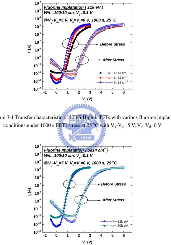
Figure 3-1 Transfer characteristic of LTPS High-k TFTs with various fluorine implant conditions under 1000 s PBTI stress at 25 oC with Vg-Vth=5 V, Vs=Vd=0 V...18
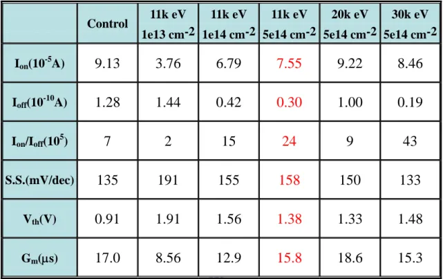
Figure 3-2 Transfer characteristic of LTPS High-k TFTs with various fluorine implant conditions under 1000 s PBTI stress at 25 oC with Vg-Vth=5 V, Vs=Vd=0 V...18
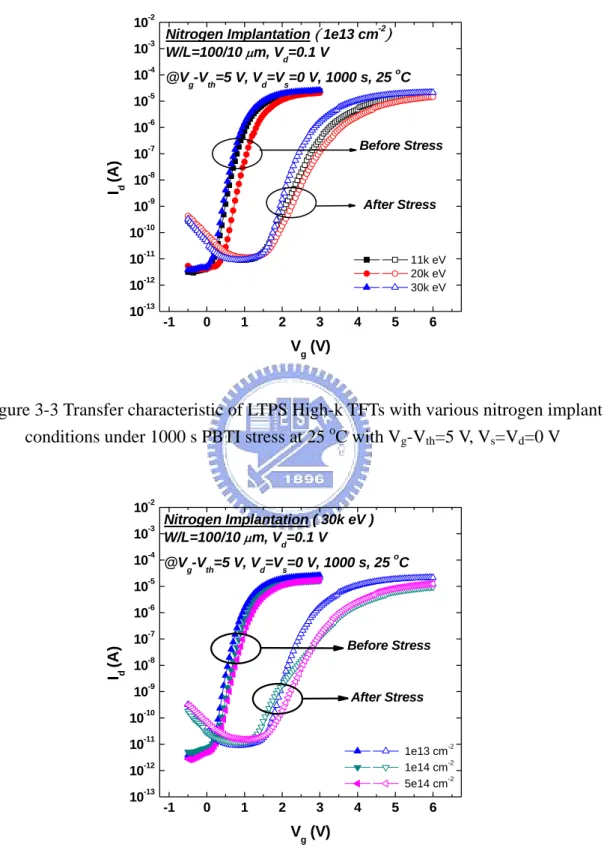
Figure 3-3 Transfer characteristic of LTPS High-k TFTs with various nitrogen implant conditions under 1000 s PBTI stress at 25 oC with Vg-Vth=5 V, Vs=Vd=0 V...22
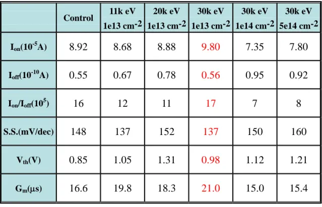
Figure 3-4 Transfer characteristic of LTPS High-k TFTs with various nitrogen implant conditions under 1000 s PBTI stress at 25 oC with Vg-Vth=5 V, Vs=Vd=0 V...22
Figure 4-1 NBTI model of interaction between poly-Si and SiO2[61] ...27
Figure 4-2 NBTI model show fluorine incorporation into poly-Si [46]...27
Figure 4-3 Defect sites in band diagram ...28
Figure 4-4 Transfer characteristic with and without fluorine implantation, before and after 1000 s hot carrier stress at 25 oC with Vg-Vth=5 V, Vd=5 V, Vs=0 V...32
Figure 4-5 Forward measurement with sweep Vg=-0.5~6 V, Vs=0 V, Vd=0.1 V ...32
Figure 4-6 Forward and reverse transfer characteristic with fluorine implantation, before and after 1000 s hot carrier stress at 25 oC with Vg-Vth=5 V, Vd=5 V, Vs=0 V, ...33
Figure 4-7 Transfer characteristic with and without the fluorine implantation, before and after 1000 s hot carrier stress at 25 oC with Vg-Vth=5 V, Vd=5 V, Vs=0 V, where solid line indicate the positive current, hallow line indicate the negative current ...33
Figure 4-8 Gate dielectric capacitance with and without fluorine implantation...34
Figure 4-9 Transconductance with and without the fluorine implantation, before and after 1000 s hot carrier stress at 25 oC with Vg-Vth=5 V, Vd=5 V, Vs=0 V ...34
Figure 4-10 Time evolution of sub-threshold swing degradation under hot carrier stress with and without fluorine implantation ...35
Figure 4-11 Time evolution of threshold voltage shift under hot carrier stress with and without fluorine implantation ...35
Figure 4-12 Transfer characteristic with and without the fluorine implantation, before and after 1000 s PBTI at 25 oC with Vg-Vth=5 V, Vd=Vs=0 V ...40
Figure 4-13 Defect pool model before states creation ...40
Figure 4-14 Defect pool model after states creation...41 Figure 4-15 Transconductance with and without the fluorine implantation, before and after 1000
s PBTI at 25 oC with Vg-Vth=5 V, Vd=Vs=0 V ...41
Figure 4-16 Time evolution of threshold voltage shift under PBTI with and without fluorine implantation ...42 Figure 4-17 Time evolution of sub-threshold swing degradation under PBTI with and without
fluorine implantation ...42 Figure 4-18 Transfer characteristic without fluorine implantation, before and after 1000 s PBTI at 25 oC and 75 oC with Vg-Vth=5 V, Vd=Vs=0 V ...43
Figure 4-19 Transfer characteristic with fluorine implantation, before and after 1000 s PBTI at 25 oC and 75 oC with Vg-Vth=5 V, Vd=Vs=0 V...43
Figure 4-20 Time evolution of threshold voltage shift in control sample with temperature of 25 oC and 75 oC...44 Figure 4-21 Time evolution of threshold voltage shift in fluorine implanted sample with
temperature of 25 oC and 75 oC ...44 Figure 4-22 Interfacial oxide growth with and without fluorine implanted poly-Si ...45 Figure 4-23 Gate dielectric capacitance with and without nitrogen implantation...49 Figure 4-24 Transconductance with and without the nitrogen implantation, before and after 1000 s hot carrier stress at 25 oC with Vg-Vth=5 V, Vd=Vs=0 V...49
Figure 4-25 Transfer characteristic with and without the nitrogen implantation, before and after 1000 s hot carrier stress at 25 oC with Vg-Vth=5 V, Vd=Vs=0 V, where solid line indicate the
positive current, hallow line indicate the negative current...50 Figure 4-26 Time evolution of threshold voltage shift under hot carrier stress with and without nitrogen implantation ...50 Figure 4-27 Time evolution of sub-threshold swing degradation under hot carrier stress with and without nitrogen implantation ...51 Figure 4-28 Transfer characteristic with and without the nitrogen implantation, before and after 1000 s PBTI at 25 oC with Vg-Vth=5 V, Vd=Vs=0 V ...55
Figure 4-29 Transconductance with and without the nitrogen implantation, before and after 1000 s PBTI at 25 oC with Vg-Vth=5 V, Vd=Vs=0 V ...55
Figure 4-30 Time evolution of threshold voltage shift under PBTI with and without nitrogen implantation ...56 Figure 4-31 Time evolution of sub-threshold swing degradation under PBTI with and without
nitrogen implantation ...56 Figure 4-32 Transfer characteristic without nitrogen implantation, before and after 1000 s PBTI at 25 oC and 75 oC with Vg-Vth=5 V, Vd=Vs=0 V ...57
Figure 4-33 Transfer characteristic with nitrogen implantation, before and after 1000 s PBTI at 25
o
Chapter 1 Introduction
1.1 Overview of Poly-Si Thin-Film Transistor (Poly-Si TFT)
Since the first Polycrystalline-Silicon Thin Film Transistor (Poly-Si TFT) was
published by C.H.Fa et al.[1] in 1966, it attracted most of the scientists who work in
the Panel Display. Therefore, many researches devoted themselves on how to improve
the performance of TFT has been started at that time. TFTs also play lots of roles in
the panel industry, like Active Matrix Liquid Crystal Display (AMLCD)[2, 3], Static
Random Access Memory (SRAMs)[4, 5], Electrical Erasable Programming Read
Only Memories (EEPROM)[6, 7], etc. And among theses applications, the application
of active matrix liquid crystal display was the major driving force to promote the
developments of Poly-Si TFTs technology.
For the skills in the prior art in TFTs, it is well know that amorphous silicon had
been a popular material to be used to fabricated on TFTs in AMLCD, due to its
compatibility with low processing temperature on large-area glass substrate. However,
there existed a disadvantage with its low electron mobility (<1 cm2/Vs), which hard to
realize the integration of the switching pixels with the peripheral driver circuit on the
same substrate to further reduce the prime cost. Recently, one solution have developed
to over come the tough problem above described is to use polycrystalline silicon to be
use as the channel film, due to its electron mobility higher than amorphous silicon. On
the other hand, poly-Si TFTs plate also have higher panel resolution than
amorphous-Si one, because it has larger aperture ratio in each pixel. Thus, how to
improve the performance of poly-Si TFTs is the most important issue so as to realize
With equal requirement of electrical characteristic to MOSFETs, TFTs also work
hard to achieve high driving current, low leakage current, low threshold voltage and
low sub-threshold swing.
To improve leakage current, there exist two ways to approach. First of all, we
need to know various leakage mechanisms, like space-charge limited flow of hole
from source to drain, thermal emission of carriers via grain boundary traps in the
depletion regions, parasitic bipolar effect, impact ionization in the drain depletion
region, band-to-band tunneling in the depletion region, and field emission via grain
boundary traps[9]. Therefore, one of the problems is the large electric field across gate
dielectric between gate and drain electrode when biasing gate voltage at leakage
current region, and the other one is lots amount of defect states in grain boundary in
the drain side junction.
Several novel device structures have been reported to reduce the leakage current
with the approach of reduce the electric field between gate and drain electrode. Past
lectures show these technologies that including Lightly Doped Drain (LDD)
structure[10-12], source overlap and drain offset structure[13-15], Field Induce Drain
(FID) structure[16], N-P-N gate structure[17], Floating Sub-Gate Structure with using
photoresist reflow[18, 19], Air Cavity structure[20], High-k Spacer Offset-Gated
structure[21], Vertical Bottom-Gate Structure[22], Gate Overlapped LDD (GOLDD)
structure[23-25], Amorphous Silicon Buffer structure[26, 27], and T-gate
Technology[28].
Except for using new structures, reducing defect states in grain boundary is also
an important method. As we know, defect states in the grain boundary or in the
interface between gate dielectric and channel serve as the trapping centers. Since free
to reduce the defects and defects related grain boundary, some effective treatment
methods have been reported to enlarge grain size and passivate the defects. First,
amorphous-silicon can be crystallizes to polycrystalline silicon typically via
SPC(solid phase crystallization)[29], ELA( excimer laser annealing)[30, 31] and
MILC(metal-induce lateral crystallization) [32]. Each of above method has its
advantages and disadvantages. Besides, in order to passivate the defect states,
introducing ions to bonding with defects have several technologies been reported, that
including plasma treatment[33-40], solid phase diffusion[41], and ionic
implantation[42-47], etc. As the trapping centers decrease, it will also help to increase
the efficiency of free carriers contributed conducting current.
1.2 Recent High-k Dielectric
Furthermore, to improve the driving current and to have better sub-threshold
swing, high-k gate dielectric is one of the solutions. There are many kinds of the
candidate materials to alter the SiO2, due to the trend of scaling down length of device,
which accompany with thinner dielectric thickness. High-k insulator can be deposited
physically thicker for the same equivalent electrical oxide thickness (EOT), thus
offering significant gate leakage current reduction, as demonstrate by several groups
[48].
In the past studies, several new high-k gate dielectric materials, like Al2O3 and
Ta2O5, were suggested to increase gate capacitance density so as to improve the
mobile carrier density in the channel region. However, the k value of Al2O3 is 9~10
and is not high enough, and the improvement of the device performance is not
apparent[49]. On the other hand, it is necessary to use a thick Ta2O5 as the gate
Consequently, Hafnium-oxide based materials, such as HfO2, HfSixOy, HfOxNy
and HfSixOyNz, have been provided with some better characteristics, that including
high-permittivity, wider band-gap, and superior thermodynamic stability on
silicon[48]. Recent researches show that only replacing gate insulator may not
sufficient for device scaling, because poly-depletion effect can not be ignore for the
sub-2-nm evolution any more. Besides, temperature for the dopant activation in the
poly-Si gate electrode is always higher than the melting point of the glass substrates,
which is not suitable for the applications of panel industry. By the way, metal gate
does not need dopant activation process, and therefore to combine metal gate with
HfO2 will have the greatest potential for the future CMOS technology[48].
These years, some reports had showed that high-k insulator used on poly-Si TFTs.
Not only for using in peripheral integral circuits TFTs[51], but also using in the
(Silicon-Oxide-Nitride-Oxide-Silicon) SONOS-Type memory of TFTs[52, 53]. As
long as TFTs combine with high-k dielectric, some excellent device performances can
be achieved, that including high driving current, low threshold voltage, and low
sub-threshold swing.
1.3 Review of Introduce Fluorine and Nitrogen
For reducing trap states in the grain boundary or in the interface, plasma
treatments could easily introduce some species, like hydrogen[36], oxygen[33, 34],
deuterium[35] by gas H2, D2, O2. And solid phase diffusion methods also reported to
introduce fluorine into poly-Si by thermal diffusion[41]. For the past reports, fluorine
and nitrogen have better performances than hydrogen, and states passivated by
hydrogen could easily dehydrogenate undergo an Aluminum alloy process.
54], it can help to realize the ideal of transfer characteristic of TFTs. On the other
hand, fluorine also passivate the deep states in the band gap of poly-Si[47], which
lead to enhance better reliability. And nitrogen also has its superiority in performance
and reliability in TFTs[37-40, 42, 43].
1.4 Motivation
To conclude and combine the advantage above described, we seek for poly-Si
TFTs with excellent performances with lower leakage current, higher driving current,
lower threshold voltage, and lower sub-threshold swing. Therefore, we take fluorine
or nitrogen and high-k insulator together into TFTs processes. And for the limited of
melting point of glass substrates, we need low temperature processes to be processed.
Gate last process would become our choice, and detail will be discussed in the chapter
2.
In addition, long-term reliability issues are always what we concerned in Thin
Film Transistor. We use the methods of Positive Bias Temperature Instability (PBTI)
and Hot Carrier Stress (HCS) stressing our device. The PBTI issue earlier major
appears in n-channel device due to the “ high ” state in the inverter operation in
CMOS circuit. To date, PBTI also play an important role in the TFTs in the panel,
which used in switching elements or in the integral circuits. To deserve to be
mentioned here, we also have the same reliability problems with high-k dielectric.
There will have more completed situations to be discussed in this thesis.
1.5 Organization of Thesis
In this section, I will show our research efforts. This thesis is organized as
introduces fluorine and nitrogen, and finally motivation are described in this section.
In chapter 2, experimental process flows, and electrical parameter extraction are
shown.
In chapter 3, the best implant conditions of fluorine and nitrogen within our
experiments were determined.
In chapter 4, since the best fluorine implant condition will be use to compare
with control sample which does not introduce fluorine. To qualify how the fluorine
can strength the reliability, Hot Carrier Stress and Positive Bias Temperature
Instability would be use to be our methods. For the later half of this chapter, the same
methods will be to play into practice in nitrogen.
Chapter 2 Experiment Method
2.1 Device Fabrication Flow
This section, we will talk about the whole device fabrication flows. First, 50 nm
undoped amorphous-Si (α-Si) was deposited on thermally oxidized Si wafer by dissociation of SiH4 gas at 550oC in a low-pressure chemical vapor deposition
(LPCVD) system. Subsequently, fluorine or nitrogen ionic was introduced into α-Si film with various energies and dosages by implantation, as list in Table 2-1 and Figure
2-1. Furthermore, control sample will have identical process except for the fluorine or
nitrogen implantation. After special species implantation, α-Si was taken into furnace for re-crystallization, which so-called solid-phase crystallization (SPC), at 600oC for
24 hours in N2 ambient, as show in Figure 2-2. Then, 480 nm thick SiO2 was
deposited by plasma-enhanced chemical vapor deposition (PECVD) for field oxide
isolation. Next, source and drain regions inside the active region was patterned for
etching oxide and to proceed to implant with phosphorous (20k eV at 5 x 10¹⁵
cm-2) ,and next, dopant activated at 600 °C for 24 hr annealing in a N2 ambient, as
show in Figure 2-3. After dopant activation, whole active region patterned for oxide
etching. Followed by standard RCA, samples deposited 50 nm HfO2 by electron-beam
evaporation system. A 400 oC 30 min furnace O2 treatment was applied to improve
the gate oxide quality. And before the TaN deposition, photoresister was coating for
the lift off method. After contact etching, devices was completed by 500 nm
Aluminum deposited by thermal evaporation system and etching, alloying. The
Energy (eV) Dosage (cm-2) 11k 20k 30k 1 x 10¹³ 1F1N, 1N1N 2F1N, 2N1N 3F1N, 3N1N 1 x 10¹⁴ 1F2N, 1N2N 2F2N, 2N2N 3F2N, 3N2N 5 x 10¹⁴ 1F3N, 1N3N 2F3N, 2N3N 3F3N, 3N3N Table 2-1 Fluorine and nitrogen implant conditions
Silicon
Buried Oxide
α-Si
Fluorine or Nitrogen
Silicon
Buried Oxide
poly-Si
Figure 2-2 Process flow – solid phase crystallization
Silicon
Buried Oxide
poly-Si
FOX
FOX
FOX
Phosphorous
HfO
2
Silicon
Buried Oxide
poly-Si
FOX
n
+
n
+
TaN
FOX
Figure 2-4 Process flow – deposited high-k and metal gate
Al
Silicon
Buried Oxide
poly-Si
FOX
TaN
Al
FOX
Al
HfO
2
n
+
n
+
2.2 Device Electrical Parameters Extraction
In this section, the electrical characteristics and the long-term tests for reliability
of different conditions, were all measured by semiconductor characterization system -
KEITHLEY 4200. Moreover, the methods of parameter extraction used in this study
are described in this section. These parameters included threshold voltage (Vth),
transconductance (Gm), sub-threshold swing (S.S.), ON current (ION), OFF current
(Ioff), ON/OFF current ratio (Ion/Ioff).
2.2.1 Threshold Voltage
Threshold Voltage (Vth) is one of the most important parameters for us to
determine whether the device is good or not. However, there are lots of ways to define
the Vth for semiconductor devices, and most of them were extracted from Ids-Vgs
curves. One of the most common Vth measurement technique is the linear
extrapolation method with the Ids-Vgs curve at low drain voltage of 50 ~ 100 mV
typically to ensure operation in the linear region[55]. In fact, curve of drain current is
not zero when gate voltage is fairly low, but it can be approached to zero with
intercept the curve of drain current to axis of gate voltage by the equation
ds
th gsi
V V =V
-2 ………..……… (Eq 2-1) Equation 2-1 is only valid to extract Vth with negligible series resistance. And usually
series resistance could be negligible when the drain voltage is low so as to keep the
channel to be operated in the linear region. The Ids-Vgs curve can be divided to two
parts by the point of Vth: Vgs above Vth is usually due to series resistance and mobility,
Vgs below Vth is contributed by sub-threshold current. It is practice to extract the Vth
transconductance versus gate voltage is a simply way. And next, linear Ids-Vgs curve
can be use to extract Vth by fit a straight line to extrapolate to Ids=0.
In this thesis, Vth is defined differ form above description and is defined by more
simply way which called constant drain current method. This method can be found in
almost the papers relate to poly-Si TFTs. The Vth obtained from this way is close to
the one extracted from linear extrapolation method. Here, constant drain current is
fixed to ds dn W I =I L × ………..………(Eq 2-2)
where Idn=100 nA for n-channel at Vds=0.1 and W, L are channel width and length
respectively. In this thesis, devices were all measured by W=100 μm, L=10 μm. Thus, Ids was fixed to 10-6 A in all our discussion.
2.2.2 Transconductance
Transconductance (Gm) is one guide for us to obtain the field effect mobility.
Since transfer characteristics of poly-Si TFTs are similar to those of MOSFETs, first
order of Ids-Vgs relation in bulk Si MOSFETs can be applied to poly-Si TFTs. The
drain current in linear region (Vds < Vgs – Vth) can be approximated as the following
equation: 2 ds FE ox gs th ds ds W 1 I C ( )[(V V )V V ] L 2 μ = − − ……… (Eq 2-3)
where W is the channel width, L is the channel length, Vth is the threshold voltage, Cox
is the gate oxide capacitance per unit area. Thus, Gm is given by
ds m FE ox ds gs I W G C ( )V V μ L ∂ = = ∂ ……….……… (Eq 2-4) Here, transconductance of devices were all measured with W=100 μm, L=10 μm at Vds=0.1 V.
2.2.3 Sub-threshold Swing and Interface State
Sub-threshold Swing (S.S.) is a typical parameter which reflects gate control
ability and also the on/off speed of a device. Swing is related to the variation of the
bending at the interface with the gate voltage[8]. The drain current in the saturation
region ( Vds >Vgs – Vth ) is expressed as the following equation:
2 ds FE ox gs th 1 W I C (V V ) 2μ L = − ……….…… (Eq 2-5)
It appears that the current abruptly vanishes while Vg is reduced to zero from the
equation above. This current is due to the weak inversion happened in the channel
between flat-band and threshold voltage, which leads to a diffuse current from source
to drain electrode. However, sub-threshold swing in TFTs also present the fact of exist
of interface states in the gate insulator/poly-Si surface. The sub-threshold swing has
been reported to be closely related to the trap states located near the mid-gap (deep
states), which originate from dangling bonds, while the mobility is more associated
with the trap states located near the band edge (tail state)[56, 57]. To evaluate the
traps original existed and the states created near the interface of gate insulator/poly-Si
channel after long-time stress, there is a way. By neglecting the depletion capacitance
in the active layer, Takashi Noguchi has report that effective interface-trap-state
density (Nit) near the poly-Si/SiO2 interface can be evaluated from the sub-threshold
swing [58-60], ox it C S.S. q N =[( )( )-1]( ) ln10 kT q ……….…… (Eq 2-6) Roughly, sub-threshold swing can tell us whether the states occur in the interface
or not. The sub-threshold swing is defined as the reciprocal of slope of the Ids-Vgs
curve in weak inversion region and as the amount of gate voltage required to increase/
-1 ds gs (logI ) S.S.= V ⎡∂ ⎤ ⎢ ∂ ⎥ ⎢ ⎥ ⎣ ⎦ ……….…… (Eq 2-7) In this thesis, the sub-threshold swing is defined as one-third of the gate voltage
required decreasing the threshold current by three orders of magnitude. The threshold
current is specified to be the drain current when the gate voltage is equal to threshold
voltage.
2.2.4 On/Off Current Ratio
In common with conventional MOSFETs, on/off current ratio is also one
important parameter to request in the transfer characteristic in TFTs. A high
performance poly-Si TFT should not only exhibit large driving current, but also low
off state current or called leakage current, is required. For a switching element, like
pixel cell, the off state is frequently encountered in normal operation. Therefore,
on/off current ratio is obviously a better evaluation parameter compared with on
current alone. The leakage current mechanism in poly-Si TFTs in more complicate
than bulk Si MOSFETs. Poly-Si exist lots of inherent defect states in the intra-grain
and inter-grain site, and most of the density of states located inside the deep level of
forbidden band-gap, and increase with the number of dangling bond increase. The
values of activation energy in poly-Si is about 0.5~0.6eV, which really close to the
mid-gap[57]. Thus, it is easy to generate leakage current via trap-assist-tunneling and
band-to-band tunneling. Generally speaking, when low drain voltage biased, leakage
current usually occur with thermal generation in the drain depletion region, and that
was increase with the thicker active region layer. However, due to the existing
numerous trap states in the poly-Si film and the large electric field locate near drain
locate in the drain side, and consequently the leakage current is highest when the
voltage between drain and gate electrode are large. In short, leakage current can affect
by several mechanisms which described above and affect the on/off current ratio
strictly.
In this thesis, the on current is defined with the method of constant overdrive
current, which gate voltage apply 1V over than the threshold voltage and drain
voltage fixed to 1V for n-channel TFTs. Since devices with different conditions in this
thesis undergo stressing progresses, constant overdrive current method is one better
choice even if the threshold voltage shift is serious. This is differ from the
conventional on current extract method which grab the maximum current of sweep
Vgs at high Vds, due to the low Vgs sweeping range in virgin measurement, which does
not want “stress” happened and this range is differ from the range after stress. Finally,
Chapter 3 Electrical Characteristic of LTPS High-k TFTs
3.1 Performance and Reliability with Fluorine Implantation
To investigate how fluorine affect the LTPS High-k TFTs, the best implant
condition should be found before compare to the control sample, which does not
implant with fluorine. To find out the best condition, not only original electric
characteristic be discussed, but also the characteristic should be analyzed after stress.
Therefore, we use the positive bias temperature stress to help us find out the best one.
With stress condition as follow: bias gate stress voltage 5 V over than threshold
voltage, both drain and source bias equal to 0 V, stress time equal to 1000 s, and
temperature of measurement are all in the room temperature. All the device dimension
we measure are gate width=100 μm and gate length=10 μm, so as to reduce the effect come from miss align gate pattern, which would lead to asymmetric of source and
drain electrode.
The measurement of transfer characteristic apply gate bias sweep from -0.5 V to
6 V, with drain voltage fixed to 0.1 V, and between stressing interval, all the
measurement are applied to linear region measurement, to prevent hot carrier which
occur under saturation region measurement. Thus, gate bias instability would simply
contribute to the variation of whole material.
Figure 3-1 show the transfer characteristic before and after 1000 s PBTI stress
with Vg-Vth=5 V, Vd=Vs=0 V, at 25 oC, with different fluorine implant dosages. The
off state current, Imin, reduce further with implant dosage increase under implant
energy 11k eV, this could be thought as the drain side junction defect states would be
implant dosage does not higher than the Si solid solubility, the fluorine we introduce
into poly-Si will not segregate out which will not lead to passivate the trap states but
generate the additional defects to degrade the electrical properties[45].
Figure 3-2 show the characteristics before and after 1000 s PBTI stress with
Vg-Vth=5 V, Vd=Vs=0 V, at 25 oC, with different fluorine implant energies. The off
state current increase with the increase of implant energy, but the larger implant
energy of 30k eV perform the lowest off state current. The latter measurement of this
sample serve serious gate leakage current, this may be due to the damage created in
the interface which does not repair after 600 oC anneal from the higher implant energy,
so that create a Flank-Pool tunneling path. Since the serious gate leakage current, we
do not present the transfer characteristic of 30k eV here.
The Table 3-1, 3-2 list the characteristic before and after PBTI stress, and Table
3-3 list the degradation percentage under the same PBTI stress. The transconductance
(Gm) increase with the implant dosages, this might due to the more fluorine ions
passivate the tail states in the grain boundary, even after PBTI stress the dosage of
5e14 cm-2 still perform best. Although the better of Gm show in the condition of 20k
eV, but it has the larger off state current, this is because of the drain side junction near
the interface does not passivated, but the states in the grain boundary been passivated
very well as show in Gm, which is due to larger implant energy accompany with
deeper passivated positions.
Finally, the best condition of 11k eV, 5e14 cm-2 has been our choice, due to the
lowest off state current, higher on/off current ratio, excellent sub-threshold swing, as
-1 0 1 2 3 4 5 6 10-13 10-12 10-11 10-10 10-9 10-8 10-7 10-6 10-5 10-4 10-3 10-2 After Stress Id (A) V g (V) 1e13 cm-2 1e14 cm-2 5e14 cm-2 Before Stress Fluorine Implatation ( 11k eV ) W/L=100/10 μm, V d=0.1 V @V g-Vth=5 V, Vd=Vs=0 V, 1000 s, 25 o C
Figure 3-1 Transfer characteristic of LTPS High-k TFTs with various fluorine implant conditions under 1000 s PBTI stress at 25 oC with Vg-Vth=5 V, Vs=Vd=0 V
-1 0 1 2 3 4 5 6 10-13 10-12 10-11 10-10 10-9 10-8 10-7 10-6 10-5 10-4 10-3 10-2 After Stress Id (A) V g (V) 11k eV 20k eV Before Stress
Fluorine Implatation ( 5e14 cm-2) W/L=100/10 μm, V d=0.1 V @V g-Vth=5 V, Vd=Vs=0 V, 1000 s, 25 o C
Figure 3-2 Transfer characteristic of LTPS High-k TFTs with various fluorine implant conditions under 1000 s PBTI stress at 25 oC with Vg-Vth=5 V, Vs=Vd=0 V
Control 11k eV 1e13 cm-2 11k eV 1e14 cm-2 11k eV 5e14 cm-2 20k eV 5e14 cm-2 30k eV 5e14 cm-2 Ion(10-5A)
9.13
3.76
6.79
7.55
9.22
8.46
Ioff(10-10A)1.28
1.44
0.42
0.30
1.00
0.19
Ion/Ioff(105)7
2
15
24
9
43
S.S.(mV/dec)135
191
155
158
150
133
Vth(V)0.91
1.91
1.56
1.38
1.33
1.48
Gm(μs)17.0
8.56
12.9
15.8
18.6
15.3
Table 3-1 Characteristics of LTPS High-k TFTs with various fluorine implant condition before 1000 s stress at 25 oC with Vg-Vth=5 V, Vs=Vd=0 V,
Control 11k eV 1e13 cm-2 11k eV 1e14 cm-2 11k eV 5e14 cm-2 20k eV 5e14 cm-2 30k eV 5e14 cm-2 Ion(10-5A)
3.37
2.16
3.73
3.27
4.44
x
Ioff(10-10A)1.77
2.08
0.79
0.45
1.28
x
Ion/Ioff(105)1
1
4
7
3
x
S.S.(mV/dec)320
278
342
250
258
x
Vth(V)2.99
3.49
3.42
3.14
3.19
x
Gm(μs)6.95 6.10
8.72
10.2
12.5
x
Table 3-2 Characteristics of LTPS High-k TFTs with various fluorine implant conditions after 1000 s stress at 25 oC with Vg-Vth=5 V, Vs=Vd=0 V,
Control 11k eV 1e13 cm-2 11k eV 1e14 cm-2 11k eV 5e14 cm-2 20k eV 5e14 cm-2 30k eV 5e14 cm-2 ΔIon(%)
-63 -57 -45
-55
-51 x
ΔIoff(%)-37 44 85
49
27 x
ΔS.S.(%)135 45 119
57
72 x
ΔVth(V)2.08 1.57 1.85
1.76
1.85 x
ΔGm(%)-59 -28 -32
-35
-32 x
Table 3-3 Characteristic degraded percentage of LTPS High-k TFTs with various fluorine implant conditions under 1000 s stress at 25 oC with Vg-Vth=5 V, Vs=Vd=0 V
3.2 Performance and Reliability with Nitrogen Implantation
To find out the best sample with introduce nitrogen by implantation, we also discuss the electrical characteristic before and after PBTI stress, with apply gate bias 5
V over than threshold voltage, and connect source and drain electrode to ground, with
stress time 1000 s, at room temperature 25 oC.
Figure 3-3 show the transfer characteristic of various nitrogen implant energy,
including 11k, 20k, 30k eV. And we could easily notice the sample with implant
energy 30k eV has the steeper sub-threshold swing after PBTI stress, this is due to
better interface recovery by nitrogen passivation.
And Figure 3-4 show the transfer characteristic with introduces different nitrogen
implant dosages but the same energy. With has larger the dosage, 1e14 cm-2, the upper
sub-threshold region which almost near the threshold voltage became smoother than
the dosage of 1e13 cm-2. This is due to the exceed nitrogen create the tail states which
original from the strain bonds in the interface. And the continuing increase the
dosages, 5e14 cm-2, the lower sub-threshold region become smoother, which is due to
the deep state creation. This results come from the exceed nitrogen do not bond with
Si, but generate dangling bonds in the interface, which do not repaired undergo 600
o
C annealing.
Moreover, the characteristics before and after BPTI stress have been list in the
Table 3-4, 3-5, and the degradation percentage is list in the Table 3-6. Since the
excellent sub-threshold swing and large value of transconductance been performed,
the condition 30k eV, 1e13 cm-2, has been our choice. This condition perform
excellent sub-threshold swing mean the interface states reduction, and also large value
-1 0 1 2 3 4 5 6 10-13 10-12 10-11 10-10 10-9 10-8 10-7 10-6 10-5 10-4 10-3 10-2 Before Stress After Stress I d (A) V g (V) 11k eV 20k eV 30k eV
Nitrogen Implantation ( 1e13 cm-2) W/L=100/10 μm, V d=0.1 V @V g-Vth=5 V, Vd=Vs=0 V, 1000 s, 25 o C
Figure 3-3 Transfer characteristic of LTPS High-k TFTs with various nitrogen implant conditions under 1000 s PBTI stress at 25 oC with Vg-Vth=5 V, Vs=Vd=0 V
-1 0 1 2 3 4 5 6 10-13 10-12 10-11 10-10 10-9 10-8 10-7 10-6 10-5 10-4 10-3 10-2 Before Stress After Stress I d (A) V g (V) 1e13 cm-2 1e14 cm-2 5e14 cm-2 Nitrogen Implantation ( 30k eV ) W/L=100/10 μm, V d=0.1 V @V g-Vth=5 V, Vd=Vs=0 V, 1000 s, 25 o C
Figure 3-4 Transfer characteristic of LTPS High-k TFTs with various nitrogen implant conditions under 1000 s PBTI stress at 25 oC with Vg-Vth=5 V,Vs=Vd=0 V
Control 11k eV 1e13 cm-2 20k eV 1e13 cm-2 30k eV 1e13 cm-2 30k eV 1e14 cm-2 30k eV 5e14 cm-2 Ion(10-5A)
8.92
8.68
8.88
9.80
7.35
7.80
Ioff(10-10A)0.55
0.67
0.78
0.56
0.95
0.92
Ion/Ioff(105)16
12
11
17
7
8
S.S.(mV/dec)148
137
152
137
150
160
Vth(V)0.85
1.05
1.31
0.98
1.12
1.21
Gm(μs)16.6
19.8
18.3
21.0
15.0
15.4
Table 3-4 Characteristics of LTPS High-k TFT with various nitrogen implant conditions before 1000 s stress at 25 oC with Vg-Vth=5 V, Vs=Vd=0 V
Control 11k eV 1e13 cm-2 20k eV 1e13 cm-2 30k eV 1e13 cm-2 30k eV 1e14 cm-2 30k eV 5e14 cm-2 Ion(10-5A)
2.55
2.85
2.40
4.26
1.95
2.30
Ioff(10-10A)0.91
1.11
1.30
1.06
1.39
1.61
Ion/Ioff(105)2
2
1
4
1
1
S.S.(mV/dec)254
326
339
202
508
327
Vth(V)2.62
3.25
3.56
2.85
3.65
3.51
Gm(μs)5.97
7.93
6.86
10.1
4.27
5.73
Table 3-5 Characteristics of LTPS High-k TFT with various nitrogen implant conditions after 1000 s stress at 25 oC with Vg-Vth=5 V, Vs=Vd=0 V
Control 11k eV 1e13 cm-2 11k eV 1e14 cm-2 11k eV 5e14 cm-2 20k eV 5e14 cm-2 30k eV 5e14 cm-2 ΔIon(%)
-71
-67
-72
-56
-73
-70
ΔIoff(%)65
64
65
86
45
72
ΔS.S.(%)72
136
122
46
238
104
ΔVth(V)1.76
2.19
2.24
1.87
2.53
2.30
ΔGm(%)-64
-60
-62
-51
-71
-63
Table 3-6 Characteristic degraded percentage of LTPS High-k TFT with various nitrogen implantation conditions under 1000 s stress at 25 oC with Vg-Vth=5 V
Chapter 4 Reliability in LTPS High-k TFTs
4.1 Brief Reliability Review
Before we discuss the reliability of hot carrier stress (HCS) and positive bias
temperature instability (PBTI), let us take a review of past studies in reliability in
TFTs. Past years, most of the reliability studies focus on hot carrier stress and
negative bias temperature instability. Among these studies, NBTI have been proposing
some models about how the interface reactions affect the electrical characteristic. The
classical model is show in Figure 4-1[61]. At high temperature, hydrogen in poly-Si
would dissociate and diffuse into SiO2, and react with SiO2 to generate OH-groups
bonded to Si atoms. Hence, defects would exist in interface or grain boundary due to
dangling bonds, in the SiO2 due to OH-groups, un-bonded positively Si atoms, and
free electrons. Since free electron would be carry away to poly-Si by electric field and
accelerate these reactions again. These years, new ideal have been proposed to
improve the poly-Si reliability under NBT operation by fluorine incorporation in
poly-Si. As show in Figure 4-2, strong Si-F bond does not broken easily and hence the
diffuse mechanism would not happen[46]. Due to the positively Si exist in the SiO2,
interface states would be easy generated by this hole trap recombination with injected
electrons, which also reported in the hot carrier stress studies[62]. Hence the
mechanism of NBTI will be more complicate than PBTI, because of hole traps will
not easily happened in SiO2. Therefore, PBTI mechanism will be simply only
contributed by electron injection.
In order to clarify the mechanisms that degrade electrical characteristics, some
mainly on intra-grain traps distributed uniformly inside the poly-Si film and also on
the deep interface states[63-65], as show in Figure 4-3 number 1. The deep states
existing in the grain boundary and oxide trap charges which do not de-trap have been
demonstrated to affect mainly on threshold voltage[63, 66, 67], as show in Figure 4-3
number 2 and 5. Tail states in the interface and/or in grain boundary mainly contribute
to the decrease of Gm maximum[63, 67], which the latest parameter to start with, as
show in Figure 4-3 number 3 and 4. Therefore, it is obvious that depending on the
nature of states generation after stress, electrical parameters can provide useful
information to clarify poly-Si TFTs degraded mechanisms under HCS and PBTI in
Figure 4-1 NBTI model of interaction between poly-Si and SiO2[61]
E
CE
VE
FPoly-Si
HfO
21
2
3
4
5
4.2 Fluorine Implantation
4.2.1 Hot Carrier Stress
First reliability test method which we use is hot carrier stress, with stress
condition by apply gate voltage 5 V over than threshold voltage, fixed drain voltage to
5 V, and connect source electrode to ground for 1000 s. Figure 4-4 show the transfer
characteristic of control sample and fluorine implanted sample. It could be easily
noticed the off state current segment in both the control and fluorine implanted
sample been disappear after hot carrier stress. We suggest the damage does not
happen in the channel, but in the gate dielectric. In order to examine our ideal,
forward and reverse drain current were measured just like the method use in the
two-bit operation memory. Figure 4-5 show the forward measurement setup, which
drain voltage fixed to 0.1 V and source connect to ground. For the reverse
measurement, source voltage fixed to 0.1 V and drain connect to ground. Figure 4-6
show the result that reverse measurement perform the off state current have the same
order as the initial reverse measurement. It means that damage happened in the drain
side gate dielectric, so that offer the frank-pool tunneling path for the current comes
from gate, which the path marked by three start sign as show in Figure 4-5. As the
gate voltage larger than drain voltage in Figure 4-4, the off state electron current will
conduct upward, tile the inversion layer electron flow into drain larger than the gate
current, and then curve again appear in the transfer characteristic. Figure 4-7 shows
the transfer characteristic again but different with the current been take for absolute
calculated, hence, the gate leakage current appeared as show in hallow sign. The
We speculate that the fluorine will diffuse into HfO2 under the gate dielectric
densify process and passivate the defect in the HfO2. Although the hot electron inject
into gate dielectric, the fluorine bond inside the HfO2 will not easy be broken. Thus
the defect created damages can be less than the control one, so that have lower gate
leakage current. And the phenomenon of fluorine passivate the defects in HfO2 also
can be see in the threshold voltage shift which is fewer than control one. Figure 4-8
show the gate dielectric capacitance of control and fluorine implanted sample, and the
fluorine implanted one have lower gate capacitance than control due to the fluorine
indeed have diffuse into gate dielectric as report in [68]. And this could also be show
at the initial Gm maximum, which has lower gate capacitance by fluorine as show in
Figure 4-9. And after hot carrier stress, the fluorine implanted sample performs the
higher Gm maximum than the control one, thanks to the strong Si-F has work in
passivate the grain boundary tail states in the drain side as discussed in the Figure 4-3.
Now let us take a look at Figure 4-10 and 4-11 which show the time evolutions
of sub-threshold swing degradation and threshold voltage shift, respectively. The time
evolution sub-threshold swing degradation of fluorine implanted sample exhibit better
than control, which contribute by strong Si-F bond passivate the interface deep states
in the drain side. And Figure 4-11 also show the fluorine implanted sample has
lowered threshold voltage shift than control, which due to the fluorine passivate the
defect states in HfO2, as discuss yet. Since sub-threshold swing region happened
earlier than the threshold voltage, the threshold voltage shift should have the same
trend with sub-threshold swing degradation, but it is not. It may be due to different
mechanisms between these two parameters. In the past studies of prediction of
threshold voltage shift, if it exhibit logarithm time dependent means that most of shift
control and fluorine implanted sample both have the same logarithm time dependent,
which suggest that our HfO2 perform the large amount of electron trapping even
though fluorine have been passivate some of these defects. Table 4-1 and 4-2 list the
characteristics before and after of control and fluorine implanted sample before and
after hot carrier stress. We could easily see the fluorine implanted sample perform the
-1 0 1 2 3 4 5 6 7 10-13 10-12 10-11 10-10 10-9 10-8 10-7 10-6 10-5 10-4 10-3 10-2 After Stress Before Stress I d (A) Vg (V) Control Fluorine
Hot Carrier Stress W/L= 100/10 μm, V d=0.1 V @ V g-Vth = 5 V, Vd=5 V, Vs=0 V, 1000 s, 25 o C
Figure 4-4 Transfer characteristic with and without fluorine implantation, before and after 1000 s hot carrier stress at 25 oC with Vg-Vth=5 V, Vd=5 V, Vs=0 V
Buried Oxide
poly-Si
TaN
HfO
2n
+n
+V
g=-0.5~6 V
V
d=0.1 V
V
s=0 V
e
-1 0 1 2 3 4 5 6 7 10-13 10-12 10-11 10-10 10-9 10-8 10-7 10-6 10-5 10-4 10-3 10-2 I d (A) Vg (V)
Forward Drain Current Reverse Drain Current
Before Stress
After Stress
Hot Carrier Stress W/L=100/10μm, V d=0.1 V @V g-Vth=5 V, Vd=5 V, Vs=0 V, 1000 s, 25 o C
Figure 4-6 Forward and reverse transfer characteristic with fluorine implantation, before and after 1000 s hot carrier stress at 25 oC with Vg-Vth=5 V, Vd=5 V, Vs=0 V,
-1 0 1 2 3 4 5 6 7 10-13 10-12 10-11 10-10 10-9 10-8 10-7 10-6 10-5 10-4 10-3 10-2 Solid + I d Hallow - Id I d (A) Vg (V) Control Fluorine Before Stress After Stress
Hot Carrier Stress W/L=100/10 μm, V d=0.1 V @V g-Vth=5 V, Vd=5 V, Vs=0 V, 1000 s, 25 o C
Figure 4-7 Transfer characteristic with and without the fluorine implantation, before and after 1000 s hot carrier stress at 25 oC with Vg-Vth=5 V, Vd=5 V, Vs=0 V, where
15 16 17 18 Control Capac it a nce (p F) Fluorine W/L=100/100 μm
Figure 4-8 Gate dielectric capacitance with and without fluorine implantation
-1 0 1 2 3 4 5 6 7 0 5 10 15 20 25 Control Fluorine After Stress Before Stress G m ( μ s ) Vg (V)
Hot Carrier Stress W/L= 100/10 μm, Vd=0.1 V
@ Vg-Vth=5 V, Vd=5 V, Vs=0 V, 1000 s, 25 oC
Figure 4-9 Transconductance with and without the fluorine implantation, before and after 1000 s hot carrier stress at 25 oC with Vg-Vth=5 V, Vd=5 V, Vs=0 V
10 100 1000 150 200 250 Subthreshold Swing under HCS @Vg-Vth=5 V, Vd=5 V, Vs=0 V, 1000 s, 25 oC S. S ( m V/ d e c ) Tstress (s) Control Fluorine
Figure 4-10 Time evolution of sub-threshold swing degradation under hot carrier stress with and without fluorine implantation
10 100 1000 0.0 0.5 1.0 1.5 2.0 Control Fluorine Δ V th (V ) Tstress (s)
Threshold Voltage Shift under HCS
@V
g-Vth=5 V, Vd=5 V, Vs=0 V, 1000 s, 25 o
C
Figure 4-11 Time evolution of threshold voltage shift under hot carrier stress with and without fluorine implantation
Control Before stress Control After stress Fluorine Before stress Fluorine After stress Ion(10-5A)
8.51
6.37
7.80
6.61
Ioff(10-10A)1.09
0.98
0.27
0.22
Ion/Ioff(105)9
6
28
29
S.S.(mV/dec)132
225
154
202
Vth(V)0.91
2.34
1.42
2.18
Gm(μs)16.4
10.3
15.1
12.3
Table 4-1 Characteristics of LTPS High-k TFTs with and without fluorine implantation before and after 1000 s hot carrier stress at 25 oC with Vg-Vth=5 V, Vd=5
V, Vs=0 V Control Fluorine ΔIon(%)
-27
-15
ΔIoff(%)-10
-18
ΔS.S.(%)70
29
ΔVth(V)1.43
0.76
ΔGm(%)-36
-18
Table 4-2 Characteristics degraded percentage of LTPS High-k TFTs with and without fluorine implantation under 1000 s hot carrier stress at 25 oC with Vg-Vth=5 V, Vd=5 V,
4.2.2 Positive Bias Temperature Instability
After discuss the hot carrier stress which happened locally in the drain side, we
look for the PBTI which qualify all the material degrade issue. Figure 4-12 show the
transfer characteristic of control and fluorine implanted sample, before and after PBTI
stress at 25 oC with Vg-Vth=5 V, Vd=Vs=0 V. One could easily see that both the drain
current of control and fluorine in the upper region of sub-threshold segment become
not steeped, and we suggest that was due to the donor like states created in the upper
of band gap[71, 72]. Figure 4-13 and 4-14 show the process of defect generated which
have the same ideal with defect pool model. Since Fermi level had been operating in
the on state for n-channel device, the band bending curve would be show like Figure
4-13. The defect states have been generated at the time device operate in channel turn
on, but the states still under Fermi level which will not contribute transfer curve. As
the time our device measure after stress, the Fermi level will move downward, and the
electron in the states will flow out and the defect states will lost the energy which
electron carry away, followed by the defect energy level move download but still
locate in the half of upper band gap. At the time we sweep the gate voltage again,
Fermi level move upward and the electron would be trapped into the states created by
stress, hence the hump in the transfer characteristic would be found. But we should
notice that this phenomenon could not be see in the hot carrier stress, due to the drain
bias in hot carrier operation will reduce the electric field upward in the drain side.
Therefore, the donor like states would generate fewer in HCS than PBTI.
Figure 4-15 show the transconductance of control and fluorine implanted sample
before and after PBTI stress. We could notice the larger Gm maximum degradation in


![Figure 4-1 NBTI model of interaction between poly-Si and SiO 2 [61]](https://thumb-ap.123doks.com/thumbv2/9libinfo/8554881.188318/38.892.205.686.198.1012/figure-nbti-model-interaction-poly-si-sio.webp)


