國
立
交
通
大
學
資訊科學與工程研究所
碩
士
論
文
應用於超高速傳輸正交多工分頻(
VHT OFDM
)系
統頻率域上之時間同步器
Robust Frequency-Domain Timing Synchronizer in the
Very-High-Throughput OFDM Systems
研 究 生:姜建安
指導教授:許騰尹 教授
應用於超高速傳輸正交多工分頻系統頻率域上之時間同步器
Robust Frequency-Domain Timing Synchronizer in the
Very-High-Throughput OFDM Systems
研 究 生:姜建安 Student:Jian-An Jiang
指導教授:許騰尹 Advisor:Terng-Yin Hsu
國 立 交 通 大 學
資 訊 科 學 與 工 程 研 究 所
碩 士 論 文
A ThesisSubmitted to Institute of Computer Science and Engineering College of Computer Science
National Chiao Tung University in partial Fulfillment of the Requirements for the Degree of Master in Computer Science
September 2010
Hsinchu, Taiwan, Republic of China
i
摘要
本論文致力於研究在 128-FFT 下超高速傳輸正交多工分頻系統(OFDM)中, 頻 率 域 上 的 時 間 同 步 器 , 並 以 全 數 位 多 相 位 時 脈 管 理 元 件 (multiphase all-digital clock management)來調整取樣相位的方式補償取樣時脈誤差。
本論文所提出的演算法,利用收到封包的前端固定格式 preambles,與理 想 preambles 之間的相關性對取樣誤差(sampling phase error)與取樣時脈偏 移(sampling clock offset)作估計以及補償。殘餘的取樣時脈偏移再利用後端
指標追蹤 (pilot tracking)作估計並補償使取樣誤差小於 8 π 。 本論文所提出的演算法,主要應用在 IEEE 所制定的無線網路標準 IEEE 802.11ad,所提出頻率域上的時間同步器在高斯雜訊及多路徑衰減的環境中, 以封包錯誤率(PER)小於 1%為標準,效能在訊號雜訊比(SNR)失去 1.4dB 下可以 達到容忍-300~400 ppm 的時脈偏移影響。
ii
Abstract
This thesis details on the design of frequency-domain synchronizer to perform coherent sampling for 128-FFT Orthogonal Frequency Division Multiplexing (OFDM) timing recovery.
The proposed algorithm focus on timing synchronization include timing acquisition, sampling clock offset (SCO) estimation and pilot tracking scheme for residual SCO. The multiphase all-digital clock management (ADCM) is utilized to adjust sampling phases estimated by timing synchronization, rather than phase-locked or delay-locked loops, and utilize the cross-correlation power between short preambles to estimation the sampling phase error and the SCO. The pilot tracking scheme tracking the gradual phase shifts caused by residual SCO and maintaining the sampling phase error <
8 π
.
The simulation platform is 802.11ad with TGad channel. Performances are measured under the TGad channel. At 1% PER and SCO tolerance range is -300~400-ppm, the SNR loss is only 0.8~1.4 dB in frequency-selective fading. From simulation results, the frequency-domain synchronizer has wide clock offset tolerance.
iii
致謝
研究所這兩年學到很多學業與做人處事上的態度,在這裡我要由衷的感謝 許多人,謝謝你們這兩年的幫助、支持與指導我才能克服種種的困難與考驗, 帶給我這兩年的充實的回憶與成長。 首先要感謝我的指導教授許騰尹教授耐心的指導,老師不僅在學業上指導 我們如何正確的研究與分析,也會把過去業界的經驗傳達我們正確的做事態 度,找出自己的價值,能在老師指導下順利畢業,我真的感到十分榮幸。 另外也感謝博士班學長與碩士班的學長姐的鼓勵與幫助,以及整個 ISIP 實 驗室成員的幫忙,真的很謝謝你們。 最後要感謝的是我親愛的家人一直在背後默默的支持我,在我低潮失落的 時候,常常因為有你們的鼓勵與陪伴,我才能克服這些考驗,現在完成這篇論 文,跟你們分享我的喜悅。iv
Table of Contents
中文摘要... i
Abstract ... ii
致謝... iii
Table of Contents ... iv
List of Figures ... v
List of Tables ... vi
Chapter 1 Introduction ... 1
1.1 Introduction ... 1
1.2 Contribution ... 2
Chapter 2 System Platform ... 3
2.1 The Basic of OFDM ... 3
2.2 IEEE 802.11ad Physical Layer Specification ... 4
2.3 Channel Model ... 7
Chapter 3 Timing Synchronization ... 10
3.1 Introduction ... 10
3.2 Coarse Sampling Clock Offset Tracking ... 11
3.3 Sampling Phase Acquisition ... 15
3.4 Pilot Tracking ... 17
3.5 Compensation ... 20
Chapter 4 Simulation Result ... 21
4.1 Simulation Platform ... 21
4.2 Simulation Result ... 22
Chapter 5 Hardware Implementation ... 25
Chapter 6 Conclusion and Future Work ... 27
v
List of Figures
Figure 0-1: IEEE 802.11ad transmitter data path ……….……. 4
Figure 2-2: IEEE 802.11ad receiver data path ……….. 4
Figure 0-3: PPDU Format ………. 6
Figure 0-4: Block diagram of channel model ……… 7
Figure 0-5: Instantaneous impulse responses ……… 8
Figure 0-6: The SCO effect of 16-QAM modulation under SCO 50 ppm ………… 9
Figure 0-1: The frequency domain timing synchronization flow ……… 10
Figure 3-2: Received signals with phase error Φ ………... 11
Figure 0-3: The symbol boundary detection architecture ………... 12
Figure 0-4: The flow of proposed sampling clock offset estimation ………….…. 13
Figure 3-5: The proposed timing detection ………....…… 16
Figure 3-6: The block diagram of frequency domain timing acquisition …………. 16
Figure 0-7: The architecture of pilot tracking scheme ……….. 18
Figure 3-8: The block diagram of compensation ……….…… 20
Figure 4.1: PDF of sampling phase error ………..…….. 22
Figure 4.2: The root mean square error of sampling phase ………..…… 23
Figure 4.3: The root mean square error of after coarse SCO tracking ………….... 23
Figure 4.4: The system performance ……….…….. 24
Figure 4.5: The offset tolerance of the FD synchronizer ………..…..……. 24
Figure 5.1: Module block diagram ………..…………. 25
vi
List of Tables
Table 0-1: Simulation parameters ……….... 21
Table 5-1: Hardware specification ……….. 26
Table 5-2: Synthesis report ……….. 26
1
Chapter 1
Introduction
1.1 Introduction
Due to the explosive growth demand for wireless communications, the next-generation wireless communication systems are expected to provide ubiquitous, high-quality, high-speed, reliable, and spectrally-efficient. However, to achieve this objective, several technical challenges have to be overcome attempt to provide high-quality service in this dynamic environment [1].
Orthogonal frequency division multiplexing (OFDM), one of the multi-carrier modulation schemes, has become the favorite modulation technology for wireless communication because of its high spectral efficiency and simplicity in equalization. However, OFDM also has its drawbacks. The notable issues of OFDM system are more sensitive to synchronization errors than single carrier system [2], [3]. Therefore, synchronization is a major task in OFDM receiver. The duties of the synchronization include packet detection, frame synchronization, timing synchronization, and frequency synchronization.
The proposed algorithm focuses on timing synchronization. The frequency domain (FD) synchronizer contains three parts: sampling phase acquisition, SCO estimation, and pilot tracking scheme for residual SCO. The sampling phase of analog to digital converter (ADC) expect to sample at the ideal sampling position
2
where it has the maximum signal power. However, SCO and sampling phase offset causes analog to digital converter is not sampled at the optimum point. Therefore, the FD synchronizer estimate and compensate the majority of SCO in FD coarse SCO tracking. The FD timing acquisition determines the initial phase offset between the transmitter and the receiver. The residual SCO results in a slowly gradual phase shifts that are proportional with time. Then, the pilot tracking scheme track the gradual phase shifts and maintain the sampling phase.
The SCO compensation in this thesis is utilizing the 2n-multiphase all-digital clock management (ADCM) to control A/D, rather than all-digital phase-locked loop (ADPLL) [9-12]. Because the large number of multiphase of ADPLL is hard to implement over several hundred MHz. a 2n-multiphase all-digital clock management (ADCM) [15] have been adopted, which is easy to produce multiphase over GHz using an in-house digital cell library. The proposed algorithm is base on the architecture and the preamble structure of IEEE 802.11ad standard
The rest of this paper is organized as follows. In Chapter 2, a brief introduction states the system description and system model. Chapter 3 describes the proposed frequency-domain timing synchronizer include sampling phase acquisition, SCO estimation, and pilot tracking scheme. Chapter 4 shows and discusses the simulation results. Conclusions are finally drawn in Chapter 5.
1.2 Contribution
This work investigate the synchronizer in frequency-domain include timing acquisition, SCO estimation and pilot tracking scheme. The proposed SCO estimation determine the majority of SCO which up to 400~-300-ppm, and the pilot tracking scheme maintain the sampling phase error less than
8 π
3
Chapter 2
System Platform
In this chapter, the basic of OFDM is introduced. Three main blocks of wireless communication: transmitter, receiver, and channel model are described as follows.
2.1 The Basic of OFDM
OFDM is a multi-carrier modulation that achieves high data rate and combat multipath fading in wireless networks. The main concept of OFDM is to divide available channel into several orthogonal sub-channels. All of the sub-channels are transmitted simultaneously, thus achieve a high spectral efficiency. Furthermore, sub-carriers have orthogonal property and carried individual data. Their spectrum overlaps are zero. It is easy to use FFT and IFFT to implementation OFDM. However, OFDM has its drawbacks. The significant one is sensitivity to synchronization errors. The synchronization errors come from two sources. One is the local oscillator frequency difference between transmitter and receiver, and the other is the Doppler spread due to the relative motion between the transmitter and the receiver [4]. In addition, timing synchronization may affect the performance of channel estimation [5].
4
2.2 IEEE 802.11ad Physical Layer Specification
2.2.1 Transmitter and Receiver
The IEEE 802.11ad provides features that can support a throughput of 1Gb/s and greater. Figure 2-1 shows transmitter data path. First use FEC encoder to encodes the source data. FEC encoder supports 1/2、5/8、3/4、13/16 four kind coding rates. The interleaver provides a form of diversity to guard against localized corruption or bursts of errors. And then, the QAM mapping is used to modulate the bit stream. It supports SQPSK, QPSK, 16 QAM, or 64 QAM. After QAM mapping, IFFT is used to transfer signal from frequency domain to time domain. In 2.538GHz, there are 128 frequency entries for each IFFT, or 128 sub-carriers in each OFDM symbol, 96 of them are data carriers, 4 of them are pilot carriers, other are null carriers. After Insert Guard Interval (GI), the signal is transmitted by RF.
Figure 2-1: IEEE 802.11ad transmitter data path [6]
Fig Figure 2-2 shows receiver data path. The signal is received from the RF. Sync is used for synchronization, including to find when exactly the packet start, the OFDM symbol boundary and the best sample phase. After a packet is presented, FFT is used to transfer received signal from time domain to frequency domain. Channel effect will be estimated and compensated by Equalizer. IQ mismatch is also taken under consideration. After all estimation and compensation, then the bit streams are de-map, de-interleaver. Finally, it is decoded by FEC which includes de-puncturing, Viterbi decoder and de-scrambler.
Fig Figure 2-2: IEEE 802.11ad receiver data path
5
2.2.2 Golay Complementary Sequence [6]
Complementary sequences which are made up of “a” and “b” parts have specific property that their out-of-phase aperiodic autocorrelation coefficients sum to zero. Each part has the length of L = 2E where E is a positive integer. The Golay complementary sequences (GCSs) Ga i and k( ) Gb i (i=0, 1, 2, … ,2k( ) k-1) are generated using the following recursive procedure:
( )
( )
( )
( )
( )
( )
(
)
( )
( )
(
)
0 0 k 1 k k 1 k 1 k 1 k k 1 k 1 Ga i i Gb i i Ga i Ga i Gb i 2 Gb i Ga i Gb i 2 − − − − − − = δ = δ = + − = − − (2.1)Where δ( )i is the Kronecker delta function.
The Short Training Field (STF) is constructed based on the Ga128( )n in the 802.11ad system, as shown in Eq. 2.1, and the Ga128 used in this platform as shown
as Eq. 2.2. Ga128 =
(2.2)
2.2.3 Basic PPDU Format
A PHY protocol data unit (PPDU) is defined to provide interoperability. Figure 2-3 shows the PPDU format for the basic OFDM mode. The OFDM frame is composed of the Short Training Field (STF), the channel estimation field (CEF), the Header, OFDM symbols and optional training fields, as shown in Figure 2-2. The
[
]
1 1 1 1 1 1 1 1 1 1 1 1 1 1 1 1 1 1 1 1 1 1 1 1 1 1 1 1 1 1 1 1 1 1 1 1 1 1 1 1 1 1 1 1 1 1 1 1 1 1 1 1 1 1 1 1 1 1 1 1 1 1 1 1 1 1 1 1 1 1 1 1 1 1 1 1 1 1 1 1 1 1 1 1 1 1 1 1 1 1 1 1 1 1 1 1 1 1 1 1 1 1 1 1 1 1 1 1 1 1 1 1 1 1 1 1 1 1 1 1 1 1 1 1 1 1 1 1 − − − − − − − − − − − − − − − − − − − − − − − − − − − − − − − − − − − − − − − − − − − − − − − − − − − − − − − − − − − − − − − −6
STF is used for packet detection, AGC, frequency offset estimation, synchronization, indication of frame type and channel estimation.
The Golay sequences are used in the STF and CEF: Ga128( )n , Gb128( )n . These are a pair of complementary sequences. The subscript denotes the length of the sequences.
The STF is composed of 14 repetitions of sequences Ga128( )n of 128 samples each, followed by a single repetition of −Ga128( )n . These samples have correlation properties. In this thesis, correlation techniques will be applicable for packet detection, symbol boundary detection, and timing synchronization. A detail data structure of L-STF is shown as Figure 2-3.
Figure 2-3: PPDU Format [6]
2.2.4 Pilot Sequence
The ideal pilots Xn k, in our platform are inserted at tones 27, 54, 78, 105. The value of the pilots at these tones is ⎣⎡ 1+ j, 1− j, 1− j, 1+ j⎤⎦ respectively. At symbol n the pilot sequence is multiplied by the value 2×pn-1, where pn is the value
generated by the polynomial S x( )=x15 +x14+ , and the sequence x1
1,x2,…x15 are
7
2.3 Channel Model
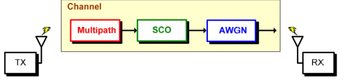
There are many imperfect effects during transmitted signals through channel, such as Additive White Gaussian Noise (AWGN), carrier frequency offset (CFO), multipath, and so on. The block diagram of channel model is shown in Figure 2-4.
Figure 2-4: Block diagram of channel model
2.3.1 Additive White Gaussian Noise
Wideband Gaussian noise comes from many natural sources, such as the thermal vibrations of atoms in antennas, "black body" radiation from the earth and other warm objects, and from celestial sources such as the sun. The AWGN channel is a good model for many satellite and deep space communication links. On the other hand, it is not a good model for most terrestrial links because of multipath, terrain blocking, interference, etc. The signal distorted by AWGN can be derived as
( ) ( ) ( )
r t =s t +n t (2.3) Where ( )r t is received signal,
( )
s t is transmitted signal, ( )
n t is AWGN.
2.3.2 Multipath
Because there are obstacles and reflectors in the wireless propagation channel, the transmitted signal arrivals at the receiver from various directions over a
8
multiplicity of paths. Such a phenomenon is called multipath. It is an unpredictable set of reflections and/or direct waves each with its own degree of attenuation and delay. Multipath is usually described by two sorts:
A. Line-of-sight (LOS): the direct connection between transmitter and receiver. B. Non-line-of-sight (NLOS): the path arriving after reflection from reflectors.
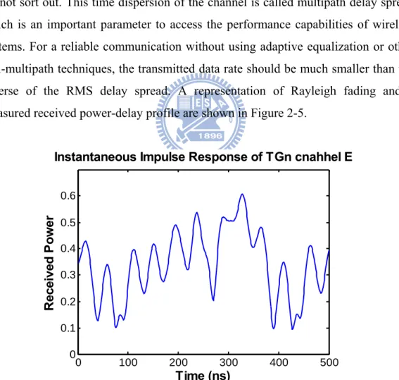
Multipath will cause amplitude and phase fluctuations, and time delay in the received signals. When the waves of multipath signals are out of phase, reduction of the signal strength at the receiver can occur. One such type of reduction is called the multipath fading; the phenomenon is known as “Rayleigh fading” or “fast fading.” Besides, multiple reflections of the transmitted signal may arrive at the receiver at different times; this can result in inter symbol interference (ISI) that the receiver cannot sort out. This time dispersion of the channel is called multipath delay spread which is an important parameter to access the performance capabilities of wireless systems. For a reliable communication without using adaptive equalization or other anti-multipath techniques, the transmitted data rate should be much smaller than the inverse of the RMS delay spread. A representation of Rayleigh fading and a measured received power-delay profile are shown in Figure 2-5.
0 100 200 300 400 500 0 0.1 0.2 0.3 0.4 0.5 0.6 Time (ns) R ecei ved P o wer
Instantaneous Impulse Response of TGn cnahhel E
Figure 2-5: Instantaneous impulse responses
9
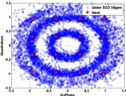
The clock drift means the different between the sampling frequency of the digital to analog converter (DAC) and the analog to digital converter (ADC). Because of sampling frequency offset, even if the initial sampling point is optimized, the following sampling points will still slowly shift with time. This model is using compress sinc waveform to cause the clock drift effect, and its effect can be written as ( ) ( )*sin ( s n) s preADC s s nT T R nT R nT c T − Δ = (2.4)
where RpreADC represents the ADC original output signal,Δ represents shift Ts sampling period and to get (R nT signal by convoluting the ADC original output s) signal and shifted sinc waveform. 錯誤! 找不到參照來源。6 shows the clock drift model effect. Initial can samples at optimum sampling points, then slightly incorrect sampling instants will cause the SNR degradation.
10
Chapter 3
Timing Synchronization
3.1 Introduction
Timing synchronization plays an important role in the receiver design of OFDM. The ADC is the first stage of baseband, so it dominates the receiving signal to noise ratio (SNR). To get the highest input SNR, the ADC is hoped to sample at the eye open position where it has the maximum signal power. However, there are symbol timing offset, sampling phase shift, sampling clock offset (SCO), and carrier frequency offset (CFO), that constitutes timing synchronization errors, so timing synchronization is necessary. The duties of the synchronization include packet detection, frame synchronization, timing synchronization, and frequency synchronization. The synchronization flow is shown in Figure 3-1. In this thesis, we will focus on timing synchronization. The FD synchronizer contains three parts: Coarse SCO tracking, sampling phase acquisition, and pilot tracking for residual SCO.
11
3.2 Coarse Sampling Clock Offset Tracking
3.2.1 Introduction
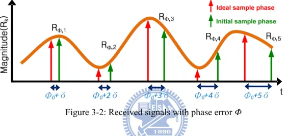
After RF down conversion and with SCO (δ) effect, all preambles and received datum (Rφ,k) are sampled by using a fixed clock phase (Φ) which may be not the ideal sampling phase, where k is the received datum index, as shown in Figure 3-2.
Figure 3-2: Received signals with phase error Φ
The phase error of received datum r[n] contains an initial constant phase offset (Φ0) between the transmitter and the receiver and the phase shift has constant
increment proportional to subcarrier index (k) and SCO (δ) as the symbol index (n) increases.
[ ] = ( r) = ( ( + ) ) = (n⋅ t t+ t)
r n r nT r n 1 δ T r T n Tδ (3.1)
where T and t Tr are the transmitter and receiver sampling period, and n Tδ t is the sampling timing offset at the nth symbol signals.
In frequency domain, the received datum with the effect due to the sampling clock offset as shown in Eq. 3.2.
2 n,k n,k n,k [ ; ] = X H δ +W s u T j πnk T R n k e (3.2)
In the following chapter described two steps to find the SCO. The first step, the parallel cross-correlation is utilized to detect the symbol boundary of the received signal. The second step, the cross-correlation power of two STFs is utilized to
12
determine the SCO.
3.2.2 Parallel Cross-correlation
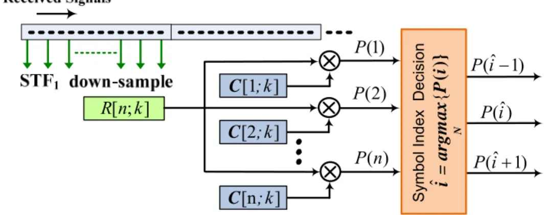
To consider the first position of the received STF, the parallel cross-correlation [13] is utilized to search for the locations of the STF which is corresponded to with the input signal, as shown in Figure 3-3.
Symbol Index Dec
ision (2) P (1) P ( ) P n ˆ ( 1) P i− ˆ ( 1) P i + ˆ ( ) P i [ ; ] R n k [1 ];k C [2 ];k C [n ];k C ˆ { N i = a rg m a x P i( )}
Figure 3-3: The symbol boundary detection architecture
If the c = {c(0), c(1),…, c(N-1)} is Short Training Field (STF) with N samples. To calculate the parallel cross-correlation of the received signal ( [ ; ]R n k ) and the known STF buffer ( [ ; ]c i k ) to be reference, the boundary correlation buffer (BCB) is designed by the ideal STF with cyclic shift like the Eq. 3.3.
1 2 3 2 1 STF(1) STF(2) STF(3) STF(N-2) STF(N-1) STF(N) ( ) STF(N) STF(1) STF(2) STF(N-3) STF(N-2) STF(N-1) ( ) STF(N-1) STF(N) STF(1) 4) 3) STF(N-( ) [ , ] ( ) ( ) ( ) " " " " " " " " " # i i i c k c k c k i k c k c k c k c − − ⎡ ⎤ ⎢ ⎥ ⎢ ⎥ ⎢ ⎥ ⎢ ⎥ =⎢ ⎥= ⎢ ⎥ ⎢ ⎥ ⎢ ⎥ ⎢ ⎥ ⎢ ⎥ ⎣ ⎦ 2) # # # % # # # # # # % # # # # # # % # STF(4) STF(5) STF(6) STF(N+1) STF(N+2) STF(N+3) STF(3) STF(4) STF(5) STF(N) STF(N+1) STF(N+2) STF(2) STF(3) STF(4) STF(N-1) STF(N) STF(N+1) # # " " " " " " " " " ⎡ ⎤ ⎢ ⎥ ⎢ ⎥ ⎢ ⎥ ⎢ ⎥ ⎢ ⎥ ⎢ ⎥ ⎢ ⎥ ⎢ ⎥ ⎢ ⎥ ⎢ ⎥ ⎢ ⎥ ⎢ ⎥ ⎢⎣ ⎦⎥ (3.3) - 2 =0 [ ] = ∑ [ ; ] C nk j π N n i;k N-1c i k e (3.4)
13
The frequency domain parallel cross-correlation power ( ( )P i ) can be obtained by
1 0 ( ) N [ ; ] [ ; ] k P i − R n k C i k = =
∑
∗ (3.5)Due to the received signals are the most likely to the ideal STF with cyclic shift (ˆi) which the cross-correlation power (P i ) is the maximum. Then, the first ( )ˆ position of the received signals is determined as shown in Eq. 3.6.
{
}
ˆ arg max ( )
N
i = P i (3.6)
Where the ideal STF with cyclic shift (C i k ) is the most likely to the received [ ; ]ˆ datum.
3.2.3 Coarse Sampling Clock Offset Tracking
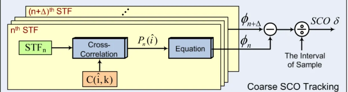
The received signals are sampled by ideal sampling phase which the cross-correlation power is the maximum. However, the SCO results that the phase shifts (φn) has constant increment proportional to subcarrier index (k) and SCO (δ) as the symbol index (n) increase. From the relation between the cross-correlation power of the nth symbol (P in( )ˆ ) and the phase error (φn), it is clear that SCO causes cross-correlation power attenuation and phase shift in the received signals.
Hence, the proposed algorithm utilizes the relation between the correlation power and the phase error to estimate the phase error caused by SCO. SCO is estimated according to the phase differences between two adjacent symbols. Figure 3-4 show the proposed coarse SCO tracking flow.
ˆ C(i, k) n
φ
SCOδ nφ
+Δ ˆ ( ) n P i14
The algorithm includes 4 steps: Step 1:
Utilize three ideal correlation powers to find an equation in two variables represented the relation between the cross-correlation power and the phase error. For enhance the similarity between the relation and the equation, we find four equations from ideal correlation powers, and average the coefficient of four equations,
2 ˆ ( )
P i =aφ +bφ+ c (3.7)
Where n is the received symbol index; ˆi is the cyclic shift of ideal STF. Step 2:
Estimate the cross-correlation powers (P in( )ˆ ) with the n symbol and the th
(n+ Δ symbol as shown in Eq. 3.8, where Δ is the interval of symbol index. )th ˆ ( ) n P i 1 0 ˆ [ ; ] [ ; ] N k R n k C i k − = =
∑
∗ (3.8) Step 3:Determine the phase error (φn) by substituting the correlation power into equation. 2 4 ( ( ))ˆ 2 n n b b a c P i a φ = − ± − − (3.9) Step 4:
Estimate the SCO (δ) by utilizing the phase differences between two adjacent symbols divide the sampling interval, where Ts is the period of one symbol.
* n n s T φ φ δ = +Δ− Δ (3.10)
15
3.3 Sampling Phase Acquisition
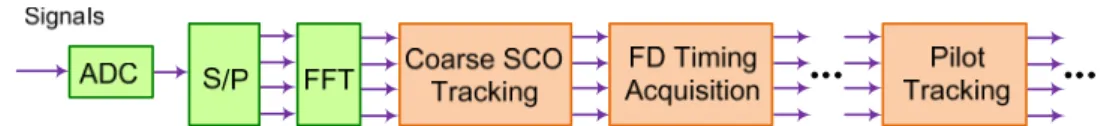
3.3.1 Frequency Domain Timing Acquisition
This section introduces 1x sampling rate timing synchronization scheme [12]. After the parallel cross-correlation and the coarse SCO tracking, the symbol boundary is known, and the majority of SCO is compensated. However, the following signals are sampled by using a fixed clock phase which may be not the ideal sampling phase. The received datum with initial phase error (Φ0) can be
obtained by Eq. 3.11.
( ; 0) = ( ) ( - ( + 0) ) and s 0∈ , | 0| 0.5≤
r n Φ x t δ t n Φ T Φ R Φ (3.11)
Where x(t) is the received signals before RF down conversion; δ(t) is the delta function; Φ0 is the sampling error; k is the subcarrier index. Then, the FFT is utilized
to get the received signal in frequency domain. - 2 =0 ( ; ) = ∑ ( ; ) nk j π N 0 0 n R k Φ N-1r n Φ e (3.12)
The Eq. 3.6 considers the cross-correlation power P i is the maximum with ( )ˆ the phase error. Due to the received signals which have the maximal cross-correlation power are sampled at the optimal phase.
The cross-correlation powers are utilized as timing detection (TD). The TD can be obtained by Eq.3.13. 0 ˆ ( , ) TD i φ = 1 0 0 ˆ [ ; ] [ ; ] N k R k φ C i k − = ∗
∑
0 ˆ ( 1, ) TD i− φ = 1 0 0 ˆ [ ; ] [ 1; ] N k R k φ C i k − = ∗ −∑
(3.13) 0 ˆ ( 1, ) TD i+ φ = 1 0 0 ˆ [ ; ] [ 1; ] N k R k φ C i k − = ∗ +∑
16 -π -π/2 0 π/2 π 1 2 3 4 0.6 0.7 0.8 0.9 1 packet Timing Decision li TD V al ue
Figure 3-5: The proposed timing detection
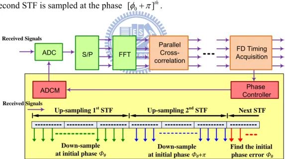
The ADCM is utilized to control A/D to sample at different phase, as shown in Figure 3-6. The first STF is sampled at the initial phase [ ]φ0 th. Then, the phase
controller adjusts the sampling clock with +π-phase changes by ADCM. After that the second STF is sampled at the phase [φ π0+ ]th.
ADCM ControllerPhase ADC
Find the initial phase error Φ0 Up-sampling 1st STF Down-sample at initial phase Φ0 Next STF Up-sampling 2nd STF Down-sample at initial phase Φ0+π Received Signals Received Signals FD Timing Acquisition Parallel Cross-correlation FFT S/P
Figure 3-6: The block diagram of frequency domain timing acquisition
The frequency domain timing acquisition determines the phase error (Φ0) on the
relation between the TD and the phase error. The one of STF C i[ˆ−1; ]k and ˆ
[ 1; ]
C i+ k which is closed to the received signals R k( ; )φ0 with phase error (Φ0)
have the larger cross-correlation power than the other. When the phase error 0 [0 ~ ]
17
ˆ [ 1; ]
C i+ k . Then, TD i(ˆ+1, )φ0 is much larger than TD i(ˆ−1, )φ0 . Similarly, when the phase error φ0∈ −[ π ~ 0] means TD i(ˆ−1, )φ0 is much larger than
0 ˆ ( 1, )
TD i+ φ . Define two conditions such as Eq. 3.14. 1 TD Δ = TD i( , )ˆφ0 − 0 ˆ ( 1, ) TD i+ φ 2 TD Δ = TD i( ,ˆ φ π0+ )− 0 ˆ ( 1, ) TD i+ φ π+ (3.14)
Whenφ0∈[0 ~ ]π , the smaller phase error Φ0, the larger ΔTD1 we estimate.
Therefore, the ratio of the relationship of ΔTD1 and TD ideal is utilized to ( ) determine the phase shift as shown as Eq. 3.15.
1 ( ) _ ( ) TD ideal TD phase shift TD ideal π − Δ = ⋅ (3.15)
Where (TD ideal is the value ) ΔTD1 in ideal sampling phase.
When φ0∈ −[ π ~ 0], the larger phase error Φ0, the smaller ΔTD2 we estimate.
Therefore, the ratio of the relationship of ΔTD2 and TD ideal is utilized to ( ) determine the phase shift as shown as Eq. 3.16.
2 _ ( ) TD phase shift TD ideal π Δ = ⋅ − (3.16)
3.4 Pilot Tracking
3.4.1 Introduction
Although the SCO in the received signals has been estimated and compensated using STF, still some residual SCO may exist. Residual SCO results in a slowly gradual phase shifts that are proportional to subcarrier indices. When the receiver operates for a long duration, the phase shifts still cause the sampling error and ICI, because the subcarriers are not orthogonal. The residual SCO estimation is inevitable in the OFDM systems.
18
differences between two pilots in two adjacent symbols to estimate the SCO. However, the accuracy of SCO estimation using pilots is base on the CFR and the SNR. Therefore, the following method is tracking the gradual phase shifts Φ and maintaining the sampling phase by utilizing the ADCM to control A/D in low SNR rather than estimating the SCO accurately.
3.4.2 Pilot Tracking
The normalized sampling error is defined as Eq. 3.17 where Tr and T are the t transmitter and receiver sampling period respectively. From Eq. 3.2, the effect of received datum caused by residual SCO is obtained by Eq. 3.18.
r t t T T T δ = − (3.17) ' 2 , , , s u nT j k T n k n k k n k
R
=
X H e
π δ+
W
(3.18)Where n is the symbol index, and kis the subcarrier index, δ' is the residual SCO,
s
T is the total symbol duration, and Tu is the useful data portion and Hkis the channel frequency response.
The proposed scheme is estimate the phase error by tracking the phase differences θ between the received pilots and the ideal pilot n k, X with the same n k, subcarrier index, the architecture as shown as Figure 3-7.
1 R(n; k ) 1 X(n; k ) Im(.) Re(.) 1 tan− 2 R(n; k ) 2 X(n; k ) Im(.) Re(.) 1 tan− (.) Avg > ΔZ Z < −Δ 8 π − 8 π
19 * , , , 2 * , , ( ) ( ( ) ) 2 s u n k n k n k nT j k T n k k n k s u X R X H X e nT k T π δ
θ
π δ
= ∠ = ∠ = (3.19)To estimate the phase differences Δθn k,Δ between the pilots in the same symbol, as shown as Eq. 3.19. For decrease the effect of noise, the pilot tracking scheme averages the phase differences Δθn k,Δ each eight symbols.
1 2 , , , 2 s n k n k n k u nT k T
θ
Δθ
θ
π δ
Δ = − = Δ (3.20)Where k1 and k2 are the index of the signals at the pilot tones.
After pilot tracking scheme, the sampling phase of ADC is expected that the sampling phase error is less than
8
π
. Due to the sampling phase error (φn) is 2πδnTs at the nth symbol. Then, substitute condition into the Eq. 3.21.
, 2 s 8 n k u u nT k k T T
π
θ
Δπ δ
Δ Δ = Δ < ⋅ (3.21)As a result, the pilot tracking scheme estimates the phase differences Δθn k,Δ continually. When the phase differences ,
8 n k u k T π θ Δ Δ
Δ ≥ ⋅ , the ADCM is utilized to adjust the A/D sampling phase
8 π
− changes in following received signals. Similarly, when the phase differences ,
8 n k u k T π θ Δ Δ
Δ ≤ − ⋅ , the ADCM is utilized to adjust the A/D sampling phase
8 π
+ changes in following received signals. Therefore, the pilot tracking scheme maintains that the sampling phase error of ADC is less than
8
π
20
3.5 Compensation
n φ 0 φ 8 π φ Δ = ±Figure 3-8: The block diagram of compensation
There are various schemes to compensate SCO, such as utilizing the interpolation techniques to resample in discrete-time domain, or rotating the FFT outputs in frequency domain, or utilizing ADPLL, ADDLL to recover ADC sampling. In the proposed algorithm, we compensate sampling phase offset and SCO in time domain with the multiphase technique which are implemented by all-digital clock management (ADCM).
After sampling phase acquisition, the algorithm outputs estimation phase Φ0 to
phase control to adjust the A/D sampling phase. Then, SCO estimation algorithm outputs a value of normalized sampling clock offset, as shown as Eq. 3.16, so we need a phase translator to get the phase offset φn correspond with the value of SCO, as shown in Eq. 3.22, where n is the data index and M is the number of multiphase.
r n t n r t t nT nT nT nT n T n M φ φ δ δ − = = − = ⋅ ⋅ = ⋅ ⋅ (3.22)
In the aspect of pilot tracking, pilot tracking will output phase 8 π
± to phase control according to the relation between phase differences and Eq. 3.21. Finally, phase control combines the three phase shift to ADCM.
21
Chapter 4
Simulation Result
We use simulation to evaluate the receiver’s performance with the AWGN, multipath fading and sampling clock offset.
4.1 Simulation Platform
MATLAB is chosen as simulation language, due to its ability to mathematics, such as matrix operation, numerous math functions, and easily drawing figures. The major parameters are shown in TABLE IV.
Table 4-1 Simulation parameters
Parameter Value
MCS Set 20
Antenna No. 1
Modulation 16 QAM
Coding Rate 3/4
PSDU Length 2048 Bytes Carrier Frequency 60 GHz
Bandwidth 2.64 GHz
IFFT / FFT Period 48.48ns(128-FFT) Table 4-2: Simulation parameters
22
4.2 Simulation Result
As mention before, the multiphase generator is used to generate 16 phases between one clock cycles. In other word, the phase error 16 means that signal is delay one cycle, and the phase error 0 means that sign is at ideal phase. With different initial phase error and SNR=5, after timing synchronizer, the final phase errors are convergence into 2 phases, as shown in Figure 4.1.
Figure 4.1: PDF of sampling phase error
Figure 4.2 shows the root mean square error of sampling phase. No synchronization means without timing acquisition to fix the unknown phase error. Those initial phase is random to generate and its RMS is about 4.5~4.8 (phase), one phase offset means the phase difference with
8
π in this simulation. The value of RMS is decreasing with the increasing of SNR and converges to 1.3 phases after timing acquisition with 400 ppm SCO.
23 -5 0 5 10 15 0 π/8 π/4 3π/8 π/2 5π/8
16-QAM Packet No=2000 PSDU=2048 bytes TGad Channel
SNR(dB)
RM
SE
Ideal with SCO=0 ppm This work with SCO=0 ppm This work with SCO=400 ppm No sync with SCO=0 ppm
Figure 4.2: The root mean square error of sampling phase
The ideal synchronization at 1% PER, SNR is about 12.7-dB under the TGad channel. So we determine the residual SCO after SCO estimation when SNR = 12.7-dB. Figure 4.3 shows the root mean square error SCO estimation and compensation. From the simulation result, SCO estimate error are about 17-ppm of SCO = 0-ppm and 19-ppm of SCO = 400-ppm after the SCO estimation.
8 9 10 11 12 13 14 15 16 0 5 10 15 20 25 30
35 16-QAM Packet No=2000 PSDU=2048 bytes TGad Channel
SNR(dB) R M SE( p p m )
SCO estimation with SCO=0 ppm SCO estimation with SCO=400 ppm Ideal SCO estimation with SCO=0 ppm
Figure 4.3: The root mean square error of after coarse SCO tracking
The required packet-error rate (PER) is 1% in 802.11ad. After timing acquisition, SCO estimation and pilot tracking scheme for residual SCO, the performance compare with perfect synchronization at 1% PER, SNR losses are about
24
0.7 dB of SCO = 0 ppm and 0.9 dB of SCO = 400 ppm, as shown in Figure 4.4.
9 10 11 12 13 14 15 16
10-3 10-2 10-1 100
16-QAM Packet NO=1000 PSDU Length=2048 bytes TGad Channel
SNR(dB)
PER
Ideal with SCO=0 ppm This work with SCO=0 ppm This work with SCO=400 ppm No sync with SCO=400 ppm
Figure 4.4: The system performance
The required packet-error rate (PER) is 1% in 802.11ad. Figure 4.5 displays the offset tolerance of the FD synchronizer include timing acquisition, SCO estimation and pilot tracking scheme with various SNR which can be as high as -300~400 ppm, much larger than the ±20 ppm in 802.11ad standard.
-700 -600 -500 -400 -300 -200 -1000 0 100 200 300 400 500 600 700 0.1 0.2 0.3 0.4 0.5 0.6 0.7 0.8 0.9 1
16-QAM Packet NO=1000 PSDU Length=2048Bytes TGad Channel
PER
sampling clock offset(ppm)
SNR=11 SNR=12 SNR=13 SNR=14 SNR=15
25
Chapter 5
Hardware Implementation
A frequency-domain synchronizer for 128-FFT OFDM systems is implemented. Figure 5.1 shows the block diagram, and figure 5.2 shows the architecture of hardware implementations, and the input are the received data after 128-FFT. In the architecture of timing synchronizer, the algorithms are described in chapter3.
Figure 5.1: Module block diagram
Figure 5.2(a): Part I. buffer, correlation, angle estimation
26
Carrier frequency Symbol interval Sample rate
× Δ =f
Figure 5.2(c): Part II. CFO estimation
Figure 5.2(d): Part II. Timing acquisition
Hardware Specification
Application IEEE 802.11ad Sample Rate 2.64 GHz Symbol Rate(After 128-FFT) 20.625 MHz
Pipeline Clock 12 ns Technology 65 nm CMOS
Table 5-1: Hardware specification
Module Name Gate Count Power
Data Buffer 41.5k 2.4294mW Correlation 75k 1.2233mW Angle 25k 0.5214mW SCO Estimation 7.5k 0.2614mW CFO Estimation 4k 0.0624mW Timing Acquisition 5k 0.0987mW Summary 158k 4.5966mW
27
Chapter 6
Conclusion and Future Work
This thesis, based on the architecture and the preamble structure of IEEE 802.11ad standard, investigate the frequency-domain timing synchronizer include timing acquisition, SCO estimation and pilot tracking scheme. Performances are measured under the TGad channel. At 1% PER and SCO tolerance range is -300~400-ppm, the SNR loss is only 0.8~1.4 dB in frequency-selective fading. From simulation results, the frequency-domain synchronizer has wide SCO tolerance.
We can improve the frequency-domain synchronizer by reducing complexity, the number of preamble and enhancing the accuracy of SCO estimation. In the thesis, we only consider the multipath and AWGN, and timing error. However, timing synchronization is in the first stage of receiver, there will be many several kinds of effects which are not improved yet. Hence, we have to improve the FD synchronizer again the tolerance of these effects in the future.
[12] [13] [18] [19] This work
System Type +64-QAM OFDM +4-QAM OFDM 64-QAM OFDM 16-QAM OFDM OFDM
+16-QAM Operation Domain Frequency Domain Frequency Domain Frequency Domain Time
domain Frequency domain
Architecture Interpolator Phase in Freq. Interpolator Interpolator Non-PLL ADCM
(ADCM)
Required Format Pilot Preamble Preamble + Pilot Pilot Preamble + Pilot
Sampling Rate N/A N/A 4x 4x 1x
Cycle Count N/A N/A N/A 100 symbols 92 symbols
(Include 6 preamble)
Tolerant
Range ±20ppm 400ppm ±200ppm ±100ppm -300 ~400 ppm
28
Bibliography
[1] T. Ojanperá and R. Prasad, "An overview of wireless broadband communications", IEEE Communications Mag., vol. 35, pp. 28-34, Jan. 1997. [2] T. Pollet, M. Van Bladel, and M. Moeneclaey, “BER sensitivity of OFDM
systems to carrier frequency offset and Wiener phase noise”, IEEE Transactions on Communications, vol. 43, pp. 191-193, Feb. /Mar. /Apr. 1995.
[3] M. Gudmundson and P.O. Anderson, “Adjacent channel interference in an OFDM system”, in Proc. Vehicular Technol. Conf., Atlanta, GA, May 1996, pp. 918-922.
[4] Hao Zhou, Malipatil A.V., Yih-Fang Huang, “Synchronization Issues in OFDM Systems”, Circuits and Systems, APCCAS 2006, pp. 988-991, Dec 2006
[5] M. Speth, S. Fechtel, G. Fock, and H. Meyr, “Optimum Receiver Design for Wireless Broad-Band Systems Using OFDM – Part I”, in IEEE Trans. on Comm., vol. 47, no. 11, pp. 1668-1677, Nov.1999.
[6] 802.11ad draft, “PHY/MAC Complete Proposal Specification”, IEEE 802.11-10/0433r2, May 2010.
[7] Theodore S.Rappaport, “Wireless Communications PRINCIPLES AND PRACTICE SECOND EDITION”, Prentice Hall PTR 2002, pp185~191.
[8] W. C. Jakes, Ed., “Microwave Mobile Communications”, IEEE Press, Piscataway, NJ, 1974
[9] J.Y. Yu, C.C. Chung, H.Y. Liu, and C.Y. Lee, “Power Reduction with Dynamic Sampling and All-Digital I/Q-Mismatch Calibration for A MB-OFDM UWB Baseband Transceiver,” IEEE Symposium on VLSI Circuits, June 2006.
[10] S. Sibecas, C.A. Emami, G. Stratis, and G. Rasor, “Pseudo-Pilot OFDM scheme for 802.11a and R/A in DSRC Applications,” IEEE VTS-Fall, VTC, Oct 2003. [11] A.I. Bo, G.E. Jian-hua, and W. Yong, “Symbol Synchronization Technique in
COFDM Systems,” IEEE Trans. Broadcasting, vol. 50, pp. 56-62, March 2004. [12] Terng-Yin Hsu, You-Hsien Lin and Ming-Feng Shen, ” Synchronous Sampling
Recovery with All-Digital Clock Management in OFDM Systems”, 2007
[13] I-Yin Liu, “The Study of Front-end Signaling and Timing Synchronization in MIMO-OFDM systems”, NCTU, master thesis, June 2007
[14] Michael Speth, Stefan Fechtel, Gunnar Fock, and Heinrich Meyr,” Optimum Receiver Design for OFDM-Based Broadband Transmission—Part II: A Case Study”,2001
[15] J.-Y. Yu, C.-C. Chung, H.-Y. Liu, Y.-W. Lin, W.-C. Liao, T.-Y. Hsu and C.-Y. Lee, "A 31.2mW UWB baseband transceiver with all-digital I/Q-mismatch calibration and dynamic sampling," IEEE symposium on VLSI Circuits, pp. 236-237, 2006.
[16] Pei-Yun Tsai,”Joint Weighted Least-Squares Estimation of Carrier-Frequency Offset and Timing Offset for OFDM Systems over Multipath Fading Channels”,
29
IEEE TRANSACTIONS ON VEHICULAR TECHNOLOGY, VOL. 54, NO. 1, JANUARY 2005
[17] Sliskovic M., “Sampling frequency offset estimation and correction in OFDM systems”, IEEE Conference on Circuits and systems, pp. 1184-1187, 2006. [18] E. Oswald, "NDA based feedforward sampling frequency synchronization for
OFDM systems," in IEEE Vehicular Technology Conference, pp. 1068-1072, 2004.
[19] M. Zhao, A. Huang, Z. Zhang and P. Qiu, "All digital tracking loop for OFDM symbol timing, ” in IEEE Vehicular Technology Conference, pp. 2435-2439, 2003.
![Figure 2-1: IEEE 802.11ad transmitter data path [6]](https://thumb-ap.123doks.com/thumbv2/9libinfo/8471728.183560/12.892.141.754.1013.1080/figure-ieee-ad-transmitter-data-path.webp)
![Figure 2-3: PPDU Format [6]](https://thumb-ap.123doks.com/thumbv2/9libinfo/8471728.183560/14.892.159.723.472.696/figure-ppdu-format.webp)