http://journals.cambridge.org Downloaded: 28 Apr 2014 IP address: 140.113.38.11
Highly oriented diamond growth on positively biased
Si substrates
Te-Fu Chang and Li Changa)
Department of Materials Science and Engineering, National Chiao Tung University, Hsinchu, Taiwan 300
(Received 25 April 2001; accepted 4 October 2001)
Deposition of highly textured diamond films on Si(001) has been achieved by using positively bias-enhanced nucleation in microwave plasma chemical vapor deposition. During the biasing period, an additional glow discharge due to the dc plasma effect appeared between the electrode and the substrate. The discharge is necessary for enhanced nucleation of diamond. X-ray diffraction, scanning electron microscopy, and cross-sectional transmission electron microscopy (XTEM) were used to characterize the microstructure of the diamond films on Si. The results show the morphology of
diamond grains in square shape with strong diamond (001) texture. XTEM reveals that an amorphous interlayer formed on the smooth Si surface before diamond nucleation.
Diamond synthesis on various substrates by chemical vapor deposition is a well-developed technique. To ob-tain highly oriented diamond films, it is necessary to generate a high density of diamond nuclei during the initial stage of diamond deposition. In general, diamond nucleation densities on mirror polished silicon substrates without any pretreatment are rarely low, less than 104cm−2. Using the so-called bias-enhanced nucleation (BEN) method in microwave plasma chemical vapor deposition (MPCVD) developed by Yugo et al., the nu-cleation density of 1010cm−2can be achieved. They re-ported that a high density of diamond was obtained at −100 V, but no growth of diamond was obtained at the positive bias condition.1 Stoner et al. reported the for-mation of an interfacial layer of –SiC and amorphous carbon on Si during the negative bias treatment.2Stoner and Glass also demonstrated that locally epitaxial dia-mond films could be successfully obtained on–SiC.3,4 Jiang and Klages first reported heteroepitaxial growth diamond on Si by negative BEN.5Since then, the nega-tive BEN method in MPCVD has been widely used to obtain heteroepitaxial diamond films on various sub-strates by many researchers.3–9Instead of using negative BEN, positive BEN in MPCVD has rarely been men-tioned. The reason could be that the result of positive BEN is not so good as negative BEN.1,10Katoch et al. have investigated both positive and negative bias effects on the nucleation of diamond in MPCVD. The nucleation
density shown in their study could reach 108cm−2under the positive bias condition, but no continuous diamond film was formed. Also the morphology of the diamond film and interfacial region between diamond and substrate were not reported.10Furthermore, no study on the orientation of diamond on positively biased Si has been published. In this letter, we report that (001) highly oriented diamond films can be deposited on mirror pol-ished silicon by applying a positive bias onto Si sub-strates. Electron microscopy shows that nucleation density of diamond is higher than 109cm−2.
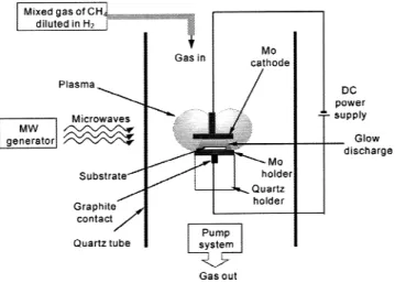
Diamond films were synthesized on mirror polished Si(001) wafers by positive BEN in a MPCVD reactor, using methane diluted in hydrogen as reactant gases. A schematic diagram of the MPCVD system under the positive dc-biased condition is shown in Fig. 1. The re-action chamber is a quartz tube with 50 mm in diameter. After reactant gases (4% CH4 diluted in hydrogen) flowed into the quartz tube, 2.45-GHz microwaves with 500-W power were input to excite the plasma. A positive dc voltage of 300 V was then applied to Si substrates. The electrode and substrate holder in a size of 2 cm in diameter are made of molybdenum. After a 20-min bi-asing pretreatment, the diamond deposition was followed by growth for 0.5–20 h with 0.667% CH4in H2. The total gas pressure was fixed at 20 torr. For the preparation of cross-sectional transmission electron microscopy (TEM) specimens, the epoxy was used to glue a sample with a dummy Si wafer as a sandwich. The sandwiched specimen was mechanically ground to a 10-m-thick foil, followed by Ar ion milling to perforation. A JEOL JEM 2010F mi-croscope (Peabody, MA) was used for microstructural characterization.
a)
Address all correspondence to this author. e-mail: [email protected]
http://journals.cambridge.org Downloaded: 28 Apr 2014 IP address: 140.113.38.11 During the positive biasing at +300 V once the
sub-strate holder was positioned within a distance of 3–5 mm from the electrode, there appeared in the plasma an ad-ditional glow discharge in purple color as the positive column often observed in direct current (dc) plasma chemical vapor deposition (CVD) between two parallel electrodes.11The purple glow discharge took on a shape like a truncated cone between the electrode and the sub-strate holder as shown in Fig. 1. The electrode was so closed to the substrate holder that it was immersed in-to plasma entirely. When the bias was switched on, the plasma shape then was distorted by the electrode because of the effect of metal exerting on plasma. Under the negative bias condition in the same setup, however, no such a glow discharge had been observed. From scanning electron microscopy (SEM) observations of the depos-ited films, it is found that the purple glow discharge is necessary to assist the diamond nucleation.
A typical SEM micrograph shown in Fig. 2 reveals the morphology of diamond on Si after 20 h of growth. Diamond grains in square shape were observed, suggesting
that a highly oriented (001) diamond film is ob-tained. The size of diamond grains is in the range of 1 to 3m. The thickness of the diamond film is about 18 m as measured from cross-sectional SEM, indicating that the deposition rate is about 0.9m/h in average. Figure 3 shows the x-ray diffraction (XRD) pattern of the same specimen. The four peaks of diamond were seen in the XRD pattern. The peaks at 2 angles of 119.4° and 44.3° are identified as the diamond (400) and (111). The ratio of integrated intensity of (400) and (111) plane for the diamond film is 34:100, compared to the ratio of 8:100 for randomly orientated powder diffraction intensity from the JCPDS data file.12The significantly increased intensity of (400) peak suggests that the diamond film possesses (001) preferred orientation, which is consistent with SEM observation in Fig. 2. The nucleation density is larger than 2 × 109cm−2as estimated from SEM ob-servations of a positive biased sample after 0.5 h growth. Figure 4(a) shows a typical cross-sectional TEM mi-crograph showing the microstructure of the diamond film on Si. It shows that the diamond film has developed into a columnar structure after growth, and the substrate sur-face is smooth. The size of the diamond grains near the interface is in the range of 30 to 50 nm, which gives the nucleation density of the order of 1010cm−2. A thin interfacial layer in white contrast was observed between the diamond film and substrate. It is noticed that the strain contrast which is often observed in negative biased samples is not seen in Si. Figure 4(b) shows the selected area diffraction (SAD) pattern from the region centered at the interface in which the Si substrate was oriented to
〈110〉 zone axis. The selected area from which the dif-fraction pattern obtained has a size of 0.5-m diameter. A diamond 111 ring can be observed from the SAD pattern. It implies that the texture of the diamond film deposited during the initial stage of deposition is not strong. However, a few strong diffraction spots as ar-rowed in the SAD pattern indicate that there may exist a certain percentage of diamond grains which are oriented. FIG. 1. Schematic diagram of MPCVD under the positive
bias-enhanced nucleation condition (not scaled).
FIG. 2. SEM micrograph of the diamond film grown on Si(100) for
20 h. FIG. 3. XRD pattern of the diamond film grown on Si(100) for 20 h.
Rapid Communications
J. Mater. Res., Vol. 16, No. 12, Dec 2001 3352
http://journals.cambridge.org Downloaded: 28 Apr 2014 IP address: 140.113.38.11 Figure 4(c) of a high-resolution TEM micrograph taken from the interfacial region shows a diamond grain misoriented with Si within 30°. The high-resolution TEM image also clearly illustrates that diamond is not directly deposited on Si. There exists a 7–10-nm-thick amor-phous interlayer between diamond and Si. In addition, the image shows that the Si substrate surface is very smooth with roughness less than 1 nm.
Kotoh et al. have proposed that carbon-containing cat-ions attack the substrate in the negative bias condition, while electrons attacked the substrate and then adsorbed carbon-containing molecules in the positive bias condi-tion.10In the present positive BEN condition, a dc glow discharge in addition to the microwave plasma only ap-pears when the distance between two parallel electrodes is close enough. Therefore, it is suggested that the effects of microwave plasma and dc plasma co-exist in this con-dition. As the deposition rate in dc plamsa CVD is quite high (approximately 20m/h),11it is likely that the nu-cleation density under the positive bias condition can be significantly increased due to the dc plasma effect ex-erted. In the negative BEN method, Si substrates are often damaged by the incident ions. As the result, the substrate surface is usually rough, and residual strain in Si exists near the surface. In contrast, the interface is very smooth after positive BEN processing, indicating the in-cident electrons result in little damage even with the applied voltage as high as 300 V.2,4–9 The relatively high-energy electrons play the major role on enhanced diamond nucleation in the positively biased method. In the negatively biased method, the nucleation density can be enhanced as well. The subplantation effect of ener-getic ions bombarding the substrate in negative biasing has been proposed to explain the BEN behavior.13 How-ever, the electrons with much smaller mass and size than ions in the plasma are unlikely to result in any subplan-tation effect on the substrate as evident for the TEM image showing no strain contrast. Therefore, we specu-late that the positive BEN might be caused by some surface-related effects such as enhanced surface diffu-sion due to electron heating or more carbon-containing species decomposed near the surface due to the strong electric field. Further support of this explanation comes from the results of electron-assisted hot-filament CVD. In electron-assisted thermal CVD, Sawabe and Inuzuka have reported that electron bombardment during growth of diamond increases the nucleation rate.14 They suggested that the role of electron bombardment is to assist the de-composition of CH4and H2at the substrate surface.
Although diamond has not directly nucleated on Si substrate, a highly oriented diamond film can still be obtained after growth. The texture becomes more pro-nounced with growth time. Therefore, a certain percent of the deposited diamond nuclei might have already ori-ented in the positive biasing stage. With evolutionary
http://journals.cambridge.org Downloaded: 28 Apr 2014 IP address: 140.113.38.11 selection during continuous deposition, the oriented
dia-mond can favorably grow further over other grains which are randomly oriented.
In summary, highly oriented diamond films can be obtained by applying a positive bias to Si substrates. The positive BEN results in a high nucleation density of dia-mond greater than 109cm−2and little damage on Si. A dc glow discharge which appears during positive BEN ap-plication in microwave plasma assists the diamond nu-cleation.
ACKNOWLEDGMENTS
We are grateful to Prof. C.F. Chen of Chiao Tung Uni-versity for providing the MPCVD facility and Prof. F.R. Chen of Tsing Hua University for TEM. The work was sponsored by the National Science Council, Republic of China, under Contract No. NSC 89-2216-E-009-033. REFERENCES
1. S. Yugo, T. Kanai, T. Kimura, and T. Muto, Appl. Phys. Lett. 58, 1036 (1991).
2. B.R. Stoner, G-H.M. Ma, S.D. Wolter, and J.T. Glass, Phys. Rev. B 45, 11067 (1992).
3. B.R. Stoner and J.T. Glass, Appl. Phys. Lett. 60, 698 (1992). 4. B.R. Stoner, G-H.M. Ma, S.D. Wolter, W. Zhu, Y-C. Wang, R.F. Davis,
and J.T. Glass, Diamond Relat. Mater. 2, 142 (1993).
5. X. Jiang and C.P. Klages, Diamond Relat. Mater. 2, 1112 (1993). 6. L. Chang, T.S. Lin, and J.L. Chen, Appl. Phys. Lett. 62, 3444
(1993).
7. B.R. Stoner, S.R. Sahaida, and J.P. Bade, J. Mater. Res. 8, 1334 (1993).
8. C.J. Chen, L. Chang, T.S. Lin, and F.R. Chen, J. Mater. Res. 10, 3041 (1995).
9. R. Stockel, M. Stammler, K. Janischowsky, and L. Ley, J. Appl. Phys. 83, 5433 (1998).
10. M. Katoh, M. Aoki, and H. Kawarada, Jpn. J. Appl. Phys. 33, L196 (1997).
11. K. Suzuki, A. Sawabe, and T. Inuzuka, Jpn. J. Appl. Phys. 29, 153 (1990).
12. Powder Diffraction File No. 06-0675, JCPDS (Joint Committee on Powder Diffraction Standard), International Centre for Diffraction Data, Newton Square, PA (1997).
13. J. Robertson, J. Gerber, S. Sattel, M. Neiler, K. Jung, and H. Ehrhardt, Appl. Phys. Lett. 66, 3287 (1995).
14. A. Sawabe and T. Inutaka, Appl. Phys. Lett. 46, 146 (1985). Rapid Communications
J. Mater. Res., Vol. 16, No. 12, Dec 2001 3354