of flip chip package using FEM-based
sensitivity analysis
Chang-Chun Lee and Kuo-Chin Chang
Taiwan Semiconductor Manufacturing Company, Ltd, Hsinchu, Taiwan, Republic of China, and
Ya-Wen Yang
Department of Applied Science and Technology, National Chiao-Tung University, Hsinchu, Taiwan, Republic of China
Abstract
Purpose – Integration of Cu/low-k interconnects into the next-generation integrated circuit chips, particularly for devices below the 90 nm technology node, has proved necessary to meet the urgent requirements of reducing RC time delay and low power consumption. Accordingly, establishment of feasible and robust packaging technology solutions in relation to the structural design, as well as material selection of the packaging components, has become increasingly important. Moreover, the nature of low-k materials and the use of lead-free solder greatly increases the complications in terms of ensuring enhanced packaging level reliability. The foregoing urgent issue needs to be quickly resolved while developing various advanced packages. This paper aims to focus on the issues.
Design/methodology/approach – The prediction model, especially for the fatigue life of lead-free solder joints, combined with virtual design of experiment with factorial analysis was used to obtain the sensitivity information of selecting geometry/material parameters in the proposed low-k flip-chip (FC) package. Moreover, a three-dimensional non-linear strip finite element model associated with the two levels of specified boundary condition of global-local technique was adopted to shorten the time of numerical calculation, as well as to give a highly accurate solution.
Findings – The results of thermal cycling in experimental testing show good agreement with the simulated analysis. In addition, the sensitivity of analysis indicates that the type of underfill material has a significant effect on the lead-free solder joint reliability.
Originality/value – A suitable combination of concerned designed factors is suggested in this research to enhance the reliability of low-k FC packaging with Pb-free solder joints.
Keywords Joining processes, Solder, Finite element analysis Paper type Research paper
Introduction
In the surface mount technology developed for electronic packaging, eutectic Sn-Pb alloy has been widely adopted in the assembly of devices to the substrate. However, increasing environmental impacts and health concerns regarding the hazard of lead has given a driving force to inhibit the use of Sn-Pb solder. Subsequently, lead-free adaptation is now necessary as per the requirements of the European Union’s Restriction of Hazardous Substances Directive. Thus, urgent requirements are necessary in the development of novel packaging materials and the modification of assembly processes in order to implement lead-free soldering (Yang et al., 2001). In order to propose the required preparations for the next-generation of advanced packaging technologies, the physics and materials challenges with regard to the effect of solder composition on the morphology of intermetallic
compounds, calculation of surface and interfacial energies, and microstructure-properties relations of Pb-free solders have been thoroughly reviewed (Tu et al., 2003). Amongst the Pb-free choices, the families of solder alloys based on the Sn-Ag and Sn-Ag-Cu (SAC) eutectic composition have emerged as those with the most potential for broad adaptation across the industry (Anderson, 2007). From the viewpoint of mechanics, the mechanical fatigue characteristics of lead-free solders, presented in the various testing conditions of low-cycle and thermal aging and so on, are one of the most important concerns in assessing the reliability of joints in future electronic packaging (Li et al., 2002; Pang et al., 2004; Shang et al., 2007). On the other hand, with regard to the packaging reliability assessment for advanced array-type packages, all kinds of solder joint fatigue models composed of stress-based, plastic strain-based, creep strain-based, energy-based, damage-based and empirical-based have been widely applied and reviewed (Lee et al., 2000). Nevertheless, choosing an approximate fatigue model for finite element (FE) modeling in accordance with the package condition is a key procedure of analysis for predicting fatigue failure. The current issue and full text archive of this journal is available at
www.emeraldinsight.com/0954-0911.htm
Soldering & Surface Mount Technology 21/1 (2009) 31 – 41
q Emerald Group Publishing Limited [ISSN 0954-0911] [DOI 10.1108/09540910910928283]
Received: 27 March 2008
Revised: 6 July 2008, 17 September 2008 Accepted: 26 September 2008
For plastic ball grid array packages, chip scale packages, and flip chip (FC) packages, many researchers have reported their investigated results concerning the reliability of lead-free solder joints. The FE modeling methods for predicting the lifetime of SnPb and SnAgCu solder joints under thermo-mechanical cycling conditions were found to offer more accurate results by means of combining constitutive law with a proper fatigue model (Ridout and Bailey, 2007). It was realized that the location of failure of lead-free solder interconnects between silicon chip and substrate under the monotonic bending test is dependent upon the combinations of opening sizes of solder mask and the categories of solder materials (Chen et al., 2007). A similar testing approach is applied in the bending fatigue reliability of lead-free and halogen-free packaging assemblies (Jonnalagadda et al., 2005). For the fatigue life prediction of solder joints, a previous work presented the Manson-Coffin fatigue life relationship and the formulations of strain range-based models for the lead-free SAC solder undergoing temperature cycling loading (Osterman and Pecht, 2007). By the demonstrations of the experimental tests, the foregoing predicted model integrated with FE analysis is suitable to various types of packages. Furthermore, the chip-packaging interaction becomes more complicated while the low-k chip is introduced. Therefore, the failure location is difficult to apprehend when various types of low-k and packaging materials are used (Wang et al., 2005; Chen et al., 2006). The analytical procedure of virtual prototyping integrated with statistics methodology was constructed to study the reliable response in the thermo-mechanical subject of electronic packages, as well as to find an optimal solution in the advanced packaging structure (van Driel et al., 2003; Vandevelde et al., 2003).
However, insufficient work has been focused on the fatigue life prediction of lead-free solder joints while the highly uncertainty of adjusting geometry/materials is expected in the design stage of packaging devices. To resolve the reliability issue, this research takes a novel structural design of low-k FC package assembling the bumps on the substrate with pre-solder material as a testing vehicle, shown in Figure 1. This test vehicle is used to implement the proposed methodology of virtual design of experiment (DOE) based on FEM. The major objective was to understand, overall, the geometry/ material impacts of packaging structure on the fatigue life of the critical lead-free solder joints by performing a three-dimensional (3D) non-linear FE modeling combined with sensitivity analysis systematically. The superiority of reliability could be enhanced through a better combination of design parameters with suitable levels suggested by the analytical results. The regression model of selecting design factors within the low-k FC package is further established.
Fundamental theory
Statistics-based sensitivity analysis of designed factors In the initial stage of developing a novel package, the effect estimation of structural sizes in geometry and adopted materials needs to be performed to obtain the information of meeting the reliability requirement. Thus, on the premise of obtaining a reliable FE model, an efficient approach having the concept of the simulation-based DOE is used to meet the disadvantage of conventional tests. Usually, the factorial design integrated with the analysis of variance (ANOVA) can
be chosen to confirm this interpretation and significance of each variable. Table I shows a list of the situation regarding the manner of ANOVA for two factors, wherea and b are the levels of the main effects A and B, respectively. The symbol, n, indicates the replicates of the test. By means of ANOVA analysis, the extents of all interaction effects among concerned factors are obvious.
Regression model
The major purpose of the regression model which combines statistical and mathematical techniques is to efficiently obtain the most precise predicted model by conducting the linear regression method. The general forms of the first-order model are expressed as follows:
y¼ b0þ i X bixiþ i,j X bixixjþ 1; ð1Þ
where bi represents the linear effect of xi, bij represents the
estimated effect of linear-by-linear interaction between xiand
xj, and1 is the fitting error. As a result of the complications in
the ANOVA and regression analysis that follows an increase in the selection of concerned factors, the experimental analysis software, named Design-Expert, is utilized to deal with the statistical mathematics.
Low-cycle fatigue analysis
For the lifetime prediction of solder joints, the Coffin-Manson relationship fatigue model is extensively used for low-cycle fatigue analysis of electronic packaging (Coffin, 1954; Manson, 1965). The mean cycles to failure, Nf, is given in the following expression:
D1gNvf ¼ A; ð2Þ
where D1g is the plastic shear strain range, and material constants of the fatigue ductility coefficient (A) and fatigue ductility exponent (v) are obtained using the least-squares method. For 96.5Sn-3.5Ag solder, A andb are 21.9 and 0.93, respectively, (Kanchanomai and Mutoh, 2004). However, more recently, researchers reported that the axial strain of solder joints has a significant influence on their fatigue behaviour, especially for FC and wafer level packages (Clech, 1999). Accordingly, for the purpose of precise estimations, the reliability prediction of FE analysis in this study takes the maximum incremental averaged equivalent plastic strainD1ep into account in an entire temperature cycle, while the convergence of hysteresis loops is achieved. By means of the relationship: D1g¼ ffiffiffi 3 p D1ep: ð3Þ
Consequently, the equation (2) for 96.5Sn-3.5Ag solder can be further rewritten in the following form:
Nf¼ 15:306 ðD1epÞ 21:075
: ð4Þ
Procedure of finite element modeling
Global-local finite element modelingIn the investigation, the commercial software, ANSYSw
, is used for the package mechanical analysis. The analytical procedures of non-linear FE simulation, combined with the global/local modeling based on the specified boundary
condition (SBC) method is performed as a result of the huge difference in the scale and geometry profile of complicated packaging structure. The other advantage of adopting the foregoing methodology is in reducing the number of elements so as to greatly shorten the calculated time. Given the proposed low-k FC package as an example, the application of the SBC method is explained in detail as follows: First, construct the global and local meshes, respectively. In the present study, the global mesh indicates the coarse mesh that models the 3D FC packaging structure. As shown in Figure 2, a 3D slice FE model with rough mesh is in accordance with the actual package sample. The package considered in this work is a FC package with a stiffener, as depicted in Figure 2(a). The stiffener, made of copper with 4 mm width and 0.8 mm thickness, is attached to the substrate to control the package deformation. The die size of the flip chip package is 16 £ 16 mm, and the thickness is 775mm (31 mils). The size of the substrate is 35 £ 35 mm, and it has a thickness of 1.18 mm. The local model with finer mesh focuses on the critical solder bump region of the packaging structure such as the outermost location furthest from the structural centre, where the expected mismatch of coefficient of thermal expansion (CTE) among device components occurs. In the meantime, the intricate components, such as multi-stacked low-k layers, pre-solder, solder mask and so on, are included
to simulate the stress/strain distribution of low-k layers and considered solder bumps (Figure 3(b)). Next, extract and interpolate nodal displacements at the global-local boundary. In the investigated FE model of the FC package shown in Figure 2(b), the nodes along the cut boundaries exhibited as all the surfaces of the concerned local model, including the outermost solder bump, are identified and the degree of freedom (DOF) values, such as displacements and potentials, at those nodes by interpolating results from the global model. For each node of the local model along the cut boundary, the ANSYSw
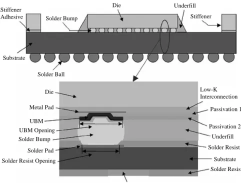
software uses the appropriate element from the coarse mesh to determine the DOF values. Owing to the global mesh having fewer nodes than the local mesh at the global-local boundary, the nodal data must be interpolated from the global mesh solution using the element shape functions when the global model is simulated. Then, the foregoing nodal displacements are given as external loadings at the boundary of the local model mesh by means of extracting and interpolating the nodal displacements from the FE result of the global model. Finally, the problem concerning the local region is analyzed. The interpolated nodal displacements constitute the boundary condition of the local problem (Figure 3(a)). Consequently, the fatigue life of the critical solder joint can be accurately predicted. The FE global and local models apply a 3D eight-node element that Figure 1 Schematic section of a Cu/low-k FC package with Pb-free solder bumps
Stiffener
Adhesive Solder Bump
Solder Bump Die Die Underfill Stiffener Low-K Interconnection Passivation 1 Passivation 2 Underfill Solder Resist Solder Resist Solder Resist Opening
UBM Opening UBM Metal Pad Solder Ball Substrate Solder Pad Solder Pad Substrate
Table I The ANOVA table for the two-factorial, fixed effects model
Source of variation Sum of squares Degrees of freedom Mean square F0
A treatments WWA a 21 MWA¼ WWA=a21 F0¼ MWA=MWE
B treatments WWB b 21 MWB¼ WWB=b21 F0¼ MWB=MWE
Interaction WWAB (a 2 1) (b 2 1) MWAB¼ WWAB=ða21Þðb21Þ F0¼ MWAB=MWE
Error WWE ab(n 2 1) MWE¼ WWE=abðn 2 1Þ N/A
provides the three directions of DOF, and consists of 20,856 elements with a total of 24,326 nodes as well as 38,798 elements with a numbers of 44,325 nodes, respectively. Through the above-mentioned FE modeling technique, integrated with the statistics-based DOE method, sensitive impacts of considered geometrical/material parameters on the solder joint reliability of low-k FC package can be obtained and discussed hereon.
Convergence analysis of sub-modeling and validation of experimental test
A 3D slice FE model has been widely employed in many researches to study the solder joint fatigue performance of FC packages for computational efficiency (Chong et al., 2003; Zhai et al., 2004; Wang et al., 2008). The 3D slice FE model, with its employed boundary conditions, is shown in Figure 2(b). Owing to the foregoing, the slice comes through the overall thickness of the packaging structure as well as occupying the chief components. The global FE model, including silicon chip, solder resist, lead-free solder joints, substrate, adhesive, low-k films, and underfill are therefore considered. Table II lists the material properties of the components utilized in the
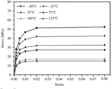
FE analysis. It should be noted that all the materials in the testing vehicle are assumed to be linear-elastic, except for the mechanical behaviour of the FC bumps (Sn-Ag) and the underfill. The temperature-dependent, stress-strain relation of the Sn-Ag solder joints is displayed in Figure 4. In addition, the influence of glass transition temperature (Tg) on underfill material is also considered to estimate the fatigue life of solder joints. Boundary conditions are carefully applied while implementing the 3D slice FE modeling. Referring to Figure 2, the detailed constrained conditions are explained as follows. The model imposes symmetry boundary conditions on one surface of the slice. This may correspond with the centre line of the solder bumps. On the other cut surface, a condition of general plane strain is imposed. Moreover, there is another symmetry plane in the yz plane where the central point of the packaging structure is located, as a result of half symmetry being assumed. Furthermore, for the purpose of preventing the occurrence of rigid body motion, all the displacements of a node at the centre and on the bottom-side surface of the package structure are constrained. To verify the appropriateness of the 3D slice global model for a package with a stiffener, Figure 2 Low-k FC package specimen: (a) top view of the package; (b) 3D slice FE model used in the global/local simulation analysis
General plane strain on this cut surface on (backside) Z Y Enlarge X Stiffener Underfill Substrate Global model Local model Symmetry on cut plane
Outermost solder bump Die (b) thickness of 3D slice Substrate Die Stiffener 3D slice (a)
the package deformation (warpage) measurement for a FC package with stiffener was carried out and the measured results were compared to the modeling prediction. One hundred and sixty-five samples were tested in the warpage measurement and the averaged warpage value is 219mm (8.62 mils) for the package subjected to a temperature testing: 150-258C. The modeling prediction is 231mm (9.09 mils). The analytical and experimental of package warpage are summarized in Table III. Table III and show that the modeling result is in good agreement with experimental measurement in warpage. Therefore, the 3D slice global model used in this study is proved to be reliable.
Under a thermal cycling load between the2 55 and 1258C using 2 cycles/hour, with 2.5 min ramping and a 10 min dwell (i.e. test environment of the JEDEC standard B and soak mode 3), all the non-linear FE simulations with full Newton-Raphson method are performed to ensure that the results of reliability predictions can be trusted. On the other hand, in
accordance with St Venant’s principle, the boundary effects of the local model are avoided by keeping the critical solder joint far away from the FE modeling edges. For this reason, the selected dimensions of the local model concerning the stability of the solution are discussed according to the numbers of solder joints from the outermost position of the silicon die. In other words, the stress and strain fields of the region of interest in the local model are not nearly affected while the edges of the local model are far away. As exhibited in Figure 5(b), a convergence in numerical solution is obtained, even though it only has the critical solder joint in the local model. However, for the purpose of preventing induction of the boundary effect, the domain size of local model with three solder joints in the study is adopted to ensure a reliable solution. Additionally, to determine the number of steady state thermal cycles used in the FE analysis, this study also calculates the maximum incremental equivalent plastic strain Figure 3 (a) 3D local FE model of critical solder bump region at silicon die corner; (b) cross-sectional sight of the detailed components at the solder bump region Die Underfill Substrate Build-up Solder Resist Substrate Core (a) Cu/Low-K Solder Bump Solder Resist Solder Pad Underfill USG Die Substrate Build-up (b)
Table II Material properties of the low-k FC package Underfill Substrate Material A a B a Build-up b Core c Adhesive d Heat spreader/stiffener e Nickel metal e CTE (ppm/ 8C) (below Tg) 32 30.1 X : 60, Y: 60, Z:6 0 X : 16, Y: 16, Z: 50 59 16.7 13.3 CTE (ppm/ 8C) (above Tg) 110 106.7 X : 135, Y: 135, Z: 160 X :5 , Y:5 , Z: 225 178 Elastic modulus (GP a) (below Tg) 7 10.73 3.5 22 11.92 at 55 8C Elastic modulus (GP a) (above Tg) 0.04 0.12 11.56 at 2 50 8C 117 205 7.95 at 0 8C 3.93 at 50 8C 0.17 at 100 8C 0.04 at 150 8C P oisson’ s ratio 0.33 0.3 0.22 0.21 0.35 0.34 0.3 Material Die e Sn-Ag solder f Solder resist g Passiv ation e Aluminum metal e Copper metal e CTE (ppm/ 8C) 2.6 21.9 55 5 23.6 16.7 Elastic modulus (GP a) 131 Non-linear and temperature dependence 2.7 270 70 68.9 P oisson’ s ratio 0.28 0.4 0.35 0.28 0.35 0.34 Notes: a Namics corporation; b Ajinomoto corporation; c Hitachi chemical corporation; d Henk el corporation; e Michael et al. , 1999 Source: f Dr Y. F. K uo; g Taiyo INK corporation
on the solder bumps for a flip chip package after 1, 2, 3, 4, and 5 thermal cycles and the results are listed in Table IV. From Table IV, the maximum incremental equivalent plastic strain reached an approximately stable state after one thermal cycle loading. Consequently, for computational efficiency, the maximum incremental equivalent plastic strain on the solder joints after one thermal cycle loading is used to evaluate the thermal fatigue life cycles of the most critical solder bump.
The simulated result indicates that the maximum equivalent plastic strain occurs on the substrate side corner of the outermost bump, far from the symmetry centre of the package structure (Figure 5(a)). An experimental procedure referred to the test environment of the JEDEC standard B and soak mode 3 was performed to verify the accuracy of global-local finite element analytical technique. In this experiment, all prepared samples were first inspected prior to the thermal cyclic test for existing failures. Later, 33 good samples were subjected to the thermal cyclic loading and then examined again for bump cracking. A resistance measurement was applied to the tested samples to detect sample failures. The experiment results reveal that the first bump failure occurred at 500 cycles for three samples and the bump failure rate is approximately 0.09. The 612 cycles estimated by equation (4) is verified by the above experimental results: the first bump failure occurred at 500 cycles (Table V) and the failure location occurred at the substrate side area of the outermost bump (Figure 6). Comparing the experimental data with the predicted thermal fatigue life from the FE analysis reveals that the present global-local FE analysis is reliable.
Figure 4 Non-linear and temperature-dependent stress and strain curve of 96.5Sn-3.5Ag lead-free solder
80 70 60 50 40 30 20 10 0 0.00 0.01 0.02 0.03 0.04 0.05 0.06 0.07 0.08 Stress (MPa) Strain Source: Kuo –40°C 25°C 100°C –25°C 75°C 125°C
Table III Comparison of package warpage
Analytical Experimental
Difference (percent) Package warpage (mm) 231 219 5
Figure 5 (a) The distribution of the incremental equivalent plastic strain for lead-free solder joints within one temperature cycle; (b) curve of numerical convergence for the numbers of Pb-free bumps in the local model of FE simulation ANSYS 10.0 Z Y X 00:16:37
AVG ELEMENT SOLUTION TIME=10 EPEQ_BP (AVG) DMX = 0.049613 SMN = 0.008477 SMX = 0.032347 0.008477 0.01113 0.013782 0.016434 0.019086 0.021738 0.02439 0.027042 0.029695 0.032347
Max. equivalent plastic strain at outermost bump
(Substrate-side corner region) (a) 0.0340 0.0335 0.0330 0.0325 0.0320 0.0315 0.0310 0.0305 0.0300 1.0 1.5 2.0 2.5 3.0 3.5 4.0
Numbers of Lead-free Solder Bump
Incremental Equivalent Plastic Strain
(b)
Table IV Comparison of maximum incremental equivalent plastic strain after different thermal cycle numbers
Thermal cycle number 1 2 3 4 5 MaxMax D1pleq(percent) 4.34 4.42 4.70 4.31 4.61
Table V Comparison of thermal fatigue life of solder joints between simulated and testing results
Experimental Predicted Thermal fatigue life (cycles) 500 612
Results and discussion
Sensitivity analysis of critical factors
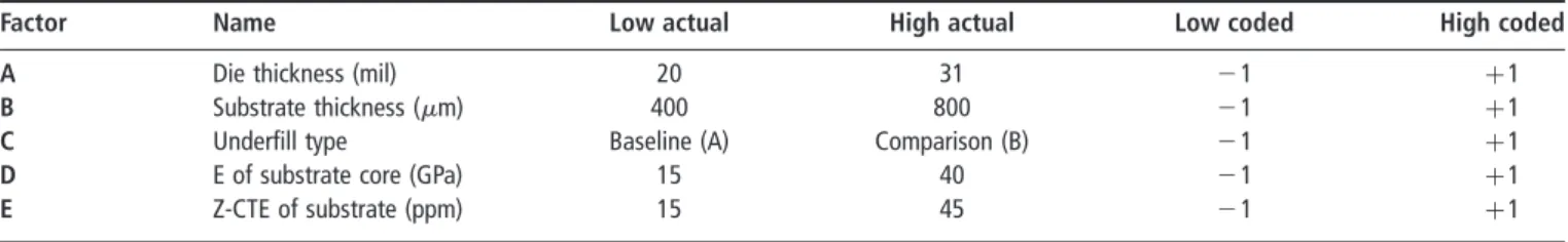
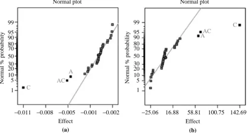
As listed in Table VI, for the purpose of obtaining the sensitivity information of each factor, the five important factors considered to affect the solder joint reliability, are selected to perform the two-level analysis of a full-factorial design with 32 runs. By means of the F distribution and normal probability plot, as shown in Table VII, and Figure 7, respectively, the importance of the effects was assessed. After screening the foregoing runs on the basis of the FE simulation, the normal plot indicates that the most significant factor is the main effect of the type of
underfill material. Next is the interaction effect between the silicon die thickness and the type of underfill material. In addition, the value of the adjusted R2 statistic is 0.8224, which implies that about 82 percent of the variability in the model composed of the significant factors can be clarified.
Interaction effect of designed factors
As the curve of baseline underfill material shown in Figure 8, the reliability of solder joints can be enhanced while the die thickness is reduced from 31 mils (775mm) to 20 mils (500mm) under the die/substrate thickness ratio from 0.43 to 0.68. However, the compared underfill material has the opposed movement and the shifted range of the calculated fatigue life that follows the change in die thickness is notable. From the foregoing situation, it could be considered that the compared underfill has a higher glass transition temperature (Tg) and elastic modulus than the baseline underfill, which could lower the substrate bending effect under the thermal loading. Using the underfill with higher Tg and elastic modulus combined with the thicker die would further increase the overall rigidity of the package and then inhibit more substrate bending effect. This results in lower strain induced at the solder bumps and thus in a higher joint fatigue life. On the contrary, a higher substrate bending occurs under the underfill with lower Tg and elastic modulus, and a thinner die bends easier with the deforming substrate. Thus, thermal fatigue life of solder joints could be enhanced because a lower thermal strain is induced. In addition, the life cycles are more sensitive to the die thickness under the compared underfill rather than the baseline underfill. Based on the above results, the structural rigidity of the package is regarded as a key factor that could affect what stress/strain behaviour occurs at Figure 6 Cross-sectional image of cracked Pb-free solder bump
Pb-free bump crack on substrate side
Table VII ANOVA results of the significant design factors for estimating the lead-free solder joint reliability of low-k FC package
Source DF Sum of squares Mean square F value Contribution (percent) (a)Incremental equivalent plastic strain
Model 3 1.384E-03 4.615E-04 48.84
A 1 1.507E-04 1.507E-04 15.95 10.88
C 1 1.043E-03 1.043E-03 110.4 75.35
AC 1 1.906E-04 1.906E-04 20.17 13.76
Residual 28 2.646E-04 9.449E-06
Cor total 31 1.649E-03
(b) Cycles Model 3 2.349E þ 5 78302.7 39.86 A 1 33735.03 33735.03 17.17 14.36 C 1 1.629E þ 5 1.629E þ 5 82.91 69.34 AC 1 38295.28 38295.28 19.49 16.30 Residual 28 55005.38 1964.48
Cor total 31 2.899E þ 5
Table VI High and low levels for each of the factors
Factor Name Low actual High actual Low coded High coded
A Die thickness (mil) 20 31 21 þ 1
B Substrate thickness (mm) 400 800 21 þ 1
C Underfill type Baseline (A) Comparison (B) 21 þ 1
D E of substrate core (GPa) 15 40 21 þ 1
solder joints under thermal deformation. Changing the die thickness for the package with high Tg and modulus underfill gives a notable consideration and superior joint reliability occurs with the high level of die thickness.
Regression model
For the purpose of observing a virtual sight to the result of interaction effect in the concerned factors, the model of response surface can be adopted to provide a practical interpretation for the foregoing results. The regression model with the form of coded factors could generate the response surface of the fatigue cycles of lead-free solder joints: Lifecycles¼ þ292:22þ32:47£Aþ71:34£C þ34:59£AC; ð5Þ where A is the die thickness, C denotes the underfill type, and AC indicates the product of factor A and factor C. In addition, because the foregoing regression model is only composed of designed factors such as the die thickness and
the underfill material type, the regression models in this study can be further represented as a function of die thickness for each type of underfill material, separately. Equations (6) and (7) show the results with the form of actual factors. Moreover, the relative 3D views of plots are revealed in Figure 9.
For baseline underfill:
Life cycles¼ þ229:73 2 0:354 £ Die Thickness: ð6Þ For compared underfill:
Life cycles¼ þ84:13 þ 11:177 £ Die Thickness:
Summary and conclusions
In order for overall understanding of the impacts of the geometry dimensions and the material properties of packaging components on the fatigue life of 96.5Sn-3.5Ag lead-free solder joints, a sensitive analysis of design factors based on 3D Figure 7 Normal probability plots: (a) the significance of the effects on the incremental equivalent plastic strain; (b) the significance of the effects on the fatigue life of the Pb-free solder joint
99 95 90 80 70 50 30 20 10 5 1 −0.011 −0.008 −0.005 −0.001 −0.002 Effect
Normal plot Normal plot
Normal % probability C AC A (a) −25.06 16.88 58.81 100.75 142.69 Effect 99 95 90 80 70 50 30 20 10 5 1 Normal % probability A C AC (b)
Figure 8 Interaction graph for the types of the underfill materials: (a) incremental equivalent plastic strain; (b) fatigue life cycles
19.00 21.00 23.00 25.00 27.00 29.00 31.00 unit: mil Die thickness (a) (b) 19.00 21.00 23.00 25.00 27.00 29.00 31.00 unit: mil Die thickness
Underfill material (Baseline) Underfill material (Compared)
Underfill material (Baseline) Underfill material (Compared)
0.0434 453 410 368 325 282 239 196 0.0402 0.0369 0.0337 0.0304
Incremental Equivalent Plastic Strain
Fatigue Life Cycle
0.0272 0.0239
non-linear FE simulation is presented in this research. In addition, both the SBC method of global-local technique and Coffin-Manson relationship regarded for 96.5Sn-3.5Ag solder material were adopted to reduce the complexity of modeling and to predict the fatigue life of Pb-free solder joints, respectively. For verifying the correctness of the presented analytical procedures, a test vehicle comprising a Pb-free FC package with a low-k chip was proposed. The data from experimental thermal cycling testing is in good agreement with the prediction of the FE modeling results. Through the ANOVA statistical and the virtual DOE sensitive analysis, the type of underfill material was identified to be the most important factor among those concerned design parameters. With a higher Tg and elastic modulus underfill, the fatigue life of solder joints can be greatly enhanced. Moreover, based on the factorial analysis results, a better combined design can be developed as a guideline to eliminate the reliability issues of Pb-free FC packages integrated with the Cu/low-k interconnect structures of the next-generation integrated circuit (IC) chips.
References
Anderson, I.E. (2007), “Development of Sn-Ag-Cu and Sn-Ag-Cu-X alloys for Pb-free electronic solder applications”, Journal of Materials Science: Materials in Electronics, Vol. 18 Nos 1/3, pp. 55-76.
Chen, K.M., Jiang, D.S., Kao, N.H. and Lai, J.Y. (2006), “Effect of underfill materials on the reliability of low-k flip-chip packaging”, Microelectronics Reliability, Vol. 46 No. 1, pp. 155-63.
Chen, Y.S., Wang, C.S., Wang, T.C., Chan, W.H., Chang, K.C. and Yuan, T.D. (2007), “Solder joint reliability assessment for flip chip ball grid array components with various designs in lead-free solder materials and solder mask dimensions”, Journal of Electronic Materials, Vol. 36 No. 1, pp. 6-16. Chong, D.Y.R., Kapoor, R. and Sun, A.Y.S. (2003),
“Reliability assessment of a high performance flip-chip BGA package (organic substrate bases) using finite element
analysis”, Proceedings of the IEEE Electronic Components and Technology Conference, New Orleans, LA, pp. 207-13. Clech, J.P. (1999), “BGA, flip-chip and CSP solder joint
reliability of the importance of model validation”, International Electronic Packaging Technical Conference and Exhibition, Maui, HI, pp. 211-17.
Coffin, L.F. Jr (1954), “A study of the effects of cyclic thermal stresses on a ductile metal”, ASME Transactions, Vol. 76, pp. 931-50.
Jonnalagadda, K., Qi, F. and Liu, J. (2005), “Mechanical bend fatigue reliability of lead-free and halogen-free PBGA assemblies”, IEEE Transactions on Components and Packaging Technologies, Vol. 28 No. 3, pp. 430-4.
Kanchanomai, C. and Mutoh, Y. (2004), “Low-cycle fatigue prediction model for Pb-free solder 96.5Sn-3.5Ag”, Journal of Electronic Materials, Vol. 33, pp. 329-33.
Lee, W.W., Nguyen, L.T. and Selvaduray, G.S. (2000), “Solder joint fatigue models: review and applicability to chip scale packages”, Microelectronics Reliability, Vol. 40 No. 2, pp. 231-44.
Li, M., Lee, K.Y., Olsen, D.R., Chen, W.T., Tan, B.T.C. and Mhaisalkar, S. (2002), “Microstructure, joint strength and failure mechanisms of SnPb and Pb-free solders in BGA packages”, IEEE Transactions on Components and Packaging Technologies, Vol. 25 No. 3, pp. 185-92.
Manson, S.S. (1965), “Mechanics”, Experimental Mechanics, Vol. 5, pp. 193-226.
Michael, G.P., Rakesh, A., Patrick, M., Terrance, D., Sirus, J. and Rahul, M. (1999), Electronic Packaging Materials and Their Properties, CRC Press LLC, New York, NY.
Osterman, M. and Pecht, M. (2007), “Strain range fatigue life assessment of lead-free solder interconnects subject to temperature cycle loading”, Soldering & Surface Mount Technology, Vol. 19 No. 2, pp. 12-17.
Pang, J.H.L., Xiong, B.S. and Low, T.H. (2004), “Low cycle fatigue models for lead-free solders”, Thin Solid Films, Vol. 462-3, pp. 408-12.
Ridout, S. and Bailey, C. (2007), “Review of methods to predict solder joint reliability under thermo-mechanical Figure 9 The response surface curve of the fatigue life cycles for the types of underfill materials: (a) baseline; (b) compared
223 222 221 220 219
Fatigue Life Cycle
Fatigue Life Cycle
Substrate thickness
unit: um Substrate thickness
unit: um 800 700 600 500 400 800 700 600 500 400 19 22 25 28 31 unit: mil Die thickness (a) (b) 19 22 25 28 31 unit: mil Die thickness 500 438 375 313 250
cycling”, Fatigue and Fracture of Engineering Material and Structures, Vol. 30 No. 5, pp. 400-12.
Shang, J.K., Zeng, Q.L., Zhang, L. and Zhu, Q.S. (2007), “Mechanical fatigue of Sn-rich Pb-free solder alloys”, Journal of Materials Science: Materials in Electronics, Vol. 18 Nos 1-3, pp. 211-27.
Tu, K.N., Gusak, A.M. and Li, M. (2003), “Physics and materials challenges for lead-free solders”, Journal of Applied Physics, Vol. 93 No. 3, pp. 1335-53.
van Driel, W.D., Zhang, G.Q., Janssen, J.H.J. and Ernst, L.J. (2003), “Response surface modeling for nonlinear packaging stresses”, Journal of Electronic Packaging, Transactions of the ASME, Vol. 125 No. 4, pp. 490-7. Vandevelde, B., Beyne, E., Zhang, G.Q., Caers, J.,
Vandepitte, D. and Baelmans, M. (2003), “Parameterized modeling of thermomechanical reliability for CSP assemblies”, Journal of Electronic Packaging, Transactions of the ASME, Vol. 125 No. 4, pp. 498-505.
Wang, G., Ho, P.S. and Groothuis, S. (2005), “Chip-packaging interaction: a critical concern for Cu/low-k packaging”, Microelectronics Reliability, Vol. 45 Nos 7/8, pp. 1079-93.
Wang, T.H., Wang, C.C., Lai, Y.S., Chang, K.C. and Lee, C.H. (2008), “Optimization of board-level thermomechanical reliability of high performance flip-chip package assembly”, Microelectronics Engineering, Vol. 85 No. 4, pp. 659-64. Yang, L., Bernstrin, J.B. and Chung, K. (2001), “The impact
of lead-free soldering on electronics packages”, Microelectronics International, Vol. 18 No. 3, pp. 20-6. Zhai, C.J., Sidharth Blish, R.C. II and Master, R.N. (2004),
“Investigation and minimization of underfill delamination in flip chip packages”, IEEE Transactions on Device and Material Reliability, Vol. 4 No. 1, pp. 86-91.
About the authors
Chang-Chun Leeis currently an R&D engineer for the Taiwan Semiconductor Manufacturing Company (TSMC), Ltd, Taiwan, ROC. He has published more than 40 journal/conference papers in the area of computational solid mechanics, advanced electronic packaging/
MEMS technology, and reliability design/analysis of IC Cu/ low-k back-end structures. He holds five Taiwan patents for wafer-level probe tests, flip chip/3D stacked wafer level packaging, and system in packaging (SIP). He likewise has two US patents pending. His recent research focuses on the robust designs of electronic packaging reliability, multiscaled modeling applications of semiconductor industry products, strained silicon engineering, phenomena analysis of stress-migration/electro-migration in advanced IC devices, as well as the interfacial fracture investigation of Cu/low-k interconnects. Chang-Chun Lee is the corresponding author and can be contacted at: d917716@alumni.nthu.edu.tw
Kuo-Chin Chang received the B.S. degree in engineering science from the National Cheng Kung University, Tainan, Taiwan, in 1993 and the PhD degree in power mechanical engineering from the National Tsing Hua University, Hsinchu, Taiwan, in 2003. He was a lecturer of power mechanical engineering at the National Tsing Hua University in 1999. He joined the Backend Technology and Service Division, Taiwan Smiconductor Manufacturing Company, Ltd, Hsinchu, Taiwan, in 2003, where he is the Technical Manager and works on modeling and design of flip chip package and wafer level package. His research interests include electronic package design and analysis, solder ball reliability and shear analysis, and the semiconductor fabrication process. He has a number of technical publications and presentations in the electronic packaging research.
Ya-Wen Yang received the B.S. degree in Department of Speech Language Pathology and Audiology from Chung Shan Medical University, Taichung, Taiwan, ROC, in 2003. She is currently pursuing the M.S. degree in department of applied science and technology, National Chiao-Tung University, Hsinchu, Taiwan. At present, she is also a speech and language pathologist in Cathy General Hospital in Taiwan. Her research interests focus on the areas of the strategies of cochlear implantation as well as the finite element analysis.
To purchase reprints of this article please e-mail: reprints@emeraldinsight.com Or visit our web site for further details: www.emeraldinsight.com/reprints