金屬銦奈米粒子之合成、氧化控制及其光學特性之研究
159
0
0
全文
(2) 金屬銦奈米粒子之合成、氧化控制 及其光學特性之研究. Novel synthesis and controlled oxidation of indium nano-particles and their optical properties. 研 究 生:吳坤翰 Student:Kun-Han WU 指導教授:陳軍華 博士 Advisor:Chun-Hua CHEN, Ph.D. 國 立 交 通 大 學 材 料 科 學 與 工 程 學系 碩 士 論 文 A Thesis Submitted to Department of Materials Science and Engineering College of Engineering National Chiao Tung University in partial Fulfillment of the Requirements for the Degree of Master In Materials Science and Engineering August 2010 Hsinchu, Taiwan, Republic of China. 中華民國九十九年八月.
(3) 致謝 在交大兩年的日子,就這麼悄悄的過去了,好像前些日子才入學不久,而現 在要離開了。兩年的研究與學習時光過得快樂又充實,修課的時候與同學互相討 論與學習;作研究的時候與老師與學長們激盪腦力探討問題與答案,在這兩年所 學到是如何獨立思考克問題所在,與如何找出答案與解決問題的能力。. 現在研究的日子即將結束了,這本論文的完成是受了許多人的幫助,實驗室 的好夥伴們幫了我許多,跟相孙學長、景筌學長他們請教不少實驗上的經驗,讓 我不至於走太多冤枉路,修誠學長在我的實驗分析上幫了大忙,也陪我熬了不少 夜,峰哥是與我一起徹夜奮戰的好夥伴,怡真學妹與沈哥則是幫我分擔不少實驗 以外的事情,宗翰學長為我解答光學上的問題,盈婷助理在我實驗很煩的時候, 會陪我們去打羽球舒解壓力,所以真的很感謝你們,若不是有你們光靠我一人, 是無法獨力完成這本研究論文的。此外特別感謝陳軍華老大對我的指導與實驗上 靈感的啟發,讓我對所研究的材料感到興趣,並嚐到研究成果所帶來的樂趣。 另外還要跟實驗室以外的學長,說聲謝謝,感謝種馬學長幫我偷進奈米 In 拍 TEM 照片,豐哥學長也幫我拍了有趣的 In2O3 結構,若缺少了 TEM 的分析,是無法 真正了解實際材料情況。. 最後僅以此論文要獻給我親愛的家人,若不是父母辛苦的養育與無條件的附 出,亦無法使我有機會來到這裡學習,另外對於早以在工作的哥哥與姊姊們,你 們也為我提供許多支持與鼓勵,你們對我的關心,我永遠記在心裡的。. 2.
(4) 摘要 本論文架構主要分為三個部分: (i) 五大類型 In 奈米結構的化學合成與結構 分析、(ii) 實心 In 奈米球體氧化動力學分析、(iii) In 奈米結構及其在不同氧化條 件下 In-In2O3 奈米核殼(core-shell)結構之光學特性。 In 奈米結構化學合成部分,本研究以基本化學還原法原理為基礎,嘗詴新穎 製程條件與步驟,成凾合成實心 In 奈米球體(Solid In nano-sphere)、多面體 In 奈 米 結 晶 (Polyhedral In nano-crystal) 、 蟲 蝕 In 奈 米 球 體 (Wormhole-like In nano-sphere)、In 奈米線(In nano-wire)、In 奈米粒子(In nano-particle)等五種各具 特色之奈米結構。 以製備所得之實心 In 奈米球體,進一步在大氣中,於 100°C、140°C、170°C、 200°C、250°C 等五個溫度下進行氧化實驗,並利用非臨場 X 光繞射技術(XRD), 定量分析其氧化比例隨時間之變化、再藉由氧化速率方程式之探討,發現奈米 In 奈米球體其氧化行為視其氧化溫度在熔點之上或下而有所不同:熔點以上溫度由 Cubic law 描述,反之熔點以下溫度則由 Parabolic law 所描述。本研究發現奈米 級 In 之氧化行為呈現二階段式氧化,亦即當氧化比例超過 60%以上時,其氧化 速率常數將下降 1~2 個數量級。此二階段氧化現象經實驗証實與高內部應力息息 相關,此內部應力來自於氧化時,氧原子之向內擴散(N 型氧化物特性),以及 金屬 In 與 In2O3 熱膨脹係數之差異。此外,本研究亦發現隨氧化層厚度的不斷增 函,導致表面應力增函誘發奈米球體破裂現象。此破裂現象隨著溫度的增函而函 劇,然而當氧化溫度昇高至 400°C 時,反而因為高溫燒結效應,彌補了表面裂縫。 在 In 奈米粒子光學方面,發現 UV-Vis 吸收峰隨尺寸而有所不同,大尺寸 (~250 nm)之 In 奈米粒子,其溶液顏色呈現深灰色;而小尺寸(~50 nm)之 In 奈米 i.
(5) 粒子,吸收峰在 290 nm,其溶液顏色為褐色。而部分氧化之實心 In 奈米球體, 其 UV-Vis 光譜則呈現純金屬電漿子效應與氧化物半導體能隙吸收之特性。其中 In2O3 層之最大吸收峰,隨氧化程度的增函而有相當明顯的紅位移現象,例如由 250°C 氧化 50 min 之 322 nm,紅位移至氧化 20 hr 之 359 nm。而 PL 光譜之分析 中發現,其發光位置多為穩定之 566 nm 橘光,而發光強度隨氧化比例的增函而 提昇。在高壓特殊氣氛下氧化所得之 In2O3,其 PL 的發光強度與波長亦有別於 上述正常大氣氧化之 566 nm 穩定橘光。. 關鍵字:In、氧化速率、應力、燒結、氧缺陷. ii.
(6) Abstract This thesis contains three main topics: (i) chemical synthesis and structural analysis of five novel Indium nanostructures, (ii) oxidation dynamics of solid Indium nano-sphere and (iii) the optical properties of the prepared In nanostructures and the In-In2O3 core-shell nano-particles partial oxidized under various conditions. Firstly, we have newly synthesized five distinct indium nanostructures including solid In nano-spheres, polyhedral In nano-crystals, wormhole-like In nano-spheres, In nano-wires, and In nano-particles using a special designed chemical reduction method. The prepared solid In nano-spheres were oxidized under atmosphere at different temperatures, 100°C, 140°C, 170°C, 200°C and 250°C. The ex-situ X-ray diffraction (XRD) patterns were repeatedly recorded and the oxidation time depedent In/In2O3 ratios were then quantatively obtained for analysis of the oxidation rate law. It is found that the oxidation behaviours can be well described with Cubic law and parabolic law for oxidation temperature above and below the melting temperature of indium bulk, respectively. A distinct two-step oxidation behavior was firstly demonstrated for the nano-scaled In spheres. The extremely high internal stress caused by the inward diffusion of oxygen atoms during oxidation (N-type oxide) as well as the thermal expansion coefficient mismatches between In and In2O3 should play as an important role for the two-step oxidation. Additionally, single or multiple cracks observed in the case of greatly oxidized In nano-spheres are reasonably considered as the relaxtion of such high internal stress. However, these cracks were re-sealed at very high oxidation temperature, e.g. 400°C, due to the sintering iii.
(7) mechanism. Optical properties including UV-Vis and PL spectra were systematically measured for the understanding of fundamentals of In and In/In2O3 core/shell nanostructures. The UV-Vis absorption spectrum shows a broaden absorption band for larger In nano-spheres (~250 nm), whereas a sharp peak around 290 nm can be found for smaller ones (~50 nm). The UV-Vis spectra of the partical oxidized In/In2O3 nano-spheres are the comprehensive absorption of the surface plasmon resonance of In metals and the optical band-gap of In2O3 semiconductors. The In2O3 thickness dependent absorption peak locates at 322 nm and 359 nm for 50 min and 20 hr oxidation time at 250°C, respectively. The PL spectra greatly vary with the oxidation conditions. For instance, a dense emission peak is typically observed around 566 nm for the case of oxidation under air, but a slight red-shifted peak over 600 nm is also frequently displayed for high pressure oxidation.. Keyword: indium; oxidation rate; stress; sintering; oxygen vacancies. iv.
(8) 目錄 中文摘要......................................................................................................i 英文摘要.................................................................................................... iii 目錄 ............................................................................................................................. v 圖表目錄.................................................................................................. viii 第一章、緒論............................................................................................................ 1 1-1. 量子限域效應(Quantum confinement effect) ................................................ 2. 1-2. 量子穿隧效應(Quantum tunnelling effect) .................................................... 3. 1-3. 庫侖阻塞效應(Coulomb blockade effect) ...................................................... 3. 1-4. 表面效應及熱、光性質(Surface effect, thermal and optical properties) ...... 4. 1-5. 研究動機與目的.............................................................................................. 6. 第二章、理論基礎與文獻回顧 ........................................................................... 8 2-1. 銦(indium)的基本性質.................................................................................... 8. 2-2. 奈米 In 之製備 ................................................................................................ 9. 2-2-1. 物理法: .................................................................................................... 9. 2-2-2. 化學法: .................................................................................................. 14. 2-3. 表面電漿共振(SPR: Surface Plasmon Resonance) ...................................... 21. 2-3-1 2-4. 奈米 In 金屬之 SPR 現象 .................................................................... 25. 金屬氧化物.................................................................................................... 30. 2-4-1. 金屬氧化物的型態 ............................................................................... 30. 2-4-2 Pilling-Bedworth rule............................................................................. 31 2-4-3 N-type、P-type 氧化物 ........................................................................ 32 2-4-5. 金屬的氧化行為 ................................................................................... 34. 2-4-6. 金屬氧化速率方程式(Rate Laws) ........................................................ 35. 2-4-7. 銦的氧化行為 ....................................................................................... 36. 2-5. In2O3 奈米結構之光致螢光(PL)特性 ........................................................... 40 v.
(9) 2-5-1. PL(Photoluminescence)發光原理 ......................................................... 40. 2-5-2. 本質、缺陷發光的差異性 ................................................................... 41. 2-5-3. In2O3 奈米結構之 PL 特性 .................................................................. 42. 第三章、實驗方法與步驟 .................................................................................. 44 3-1. 實驗藥品........................................................................................................ 44. 3-2. 實驗設備........................................................................................................ 45. 3-3. 實驗方法........................................................................................................ 46. 3-3-1. 奈米 In 之合成 ...................................................................................... 46. 3-3-2. 實心 In 奈米球體(Solid In nano-sphere)製備方法 .............................. 47. 3-3-3. 多面體 In 奈米結晶(Polyhedral In nano-crystal)製備方法 ................. 48. 3-3-4. 蟲蝕 In 奈米球體(Wormhole-like In nano-sphere)製備方法 .............. 49. 3-3-5. In 奈米線(In nano-wire)製備方法 ........................................................ 50. 3-3-6. In 奈米粒子(In nano-particle)製備方法 ............................................... 51. 3-4. 奈米 In 之氧化實驗 ...................................................................................... 52. 3-4-1 3-5. In-In2O3( core-shell )奈米粒子之合成.................................................. 52. 奈米 In 與奈米 In-In2O3 粒子之鑑定與分析 ............................................... 53. 3-5-1 X-Ray 繞射分析 .................................................................................... 53 3-5-2. 紫外光-可見光吸收光譜(UV-Vis) ....................................................... 53. 3-5-3. 場發射掃描式電子顯微鏡(FE-SEM)................................................... 54. 3-5-4. 場發射穿透式電子顯微鏡(FE-TEM) .................................................. 54. 3-5-5. 光激發螢光光譜儀(PL) ........................................................................ 55. 第四章、實驗結果與討論 .................................................................................. 57 4-1. In 奈米結構之合成與形貌結構分析 ........................................................... 57. 4-1-1. 實心 In 奈米球體(Solid In Nano-sphere) ............................................. 60. 4-1-2. 多面體 In 奈米結晶(Polyhedral In Nano-crystal) ................................ 62. 4-1-3. 蟲蝕 In 奈米球體(Wormhole-like In Nano-sphere) ............................. 66. 4-1-4. In 奈米線(In nano-wire) ........................................................................ 70. 4-1-5. In 奈米粒子(In Nano-particle) .............................................................. 73. 4-2. In 奈米粒子的氧化探討 ............................................................................... 78. 4-2-1. In 奈米粒子之氧化動力學 ................................................................... 78. 4-2-2. In 奈米粒子氧化動力分析 ................................................................... 88 vi.
(10) 4-3. In 與 In-In2O3 奈米結構之光學分析 .......................................................... 103. 4-3-1. In 奈米結構之光學分析 ..................................................................... 103. 4-3-2. In-In2O3(core-shell)奈米結構之光學分析.......................................... 109. 第五章、結論........................................................................................................ 125 第六章、未來展望 .............................................................................................. 127 參考文獻 ................................................................................................................. 128 附錄 氧化百分比之 XRD 模擬計算 ............................................................................ 136 Rietveld 模擬分析 ............................................................................................... 138 團聚成片狀 In 奈米結構...................................................................................... 141 In2O3 奈米粒子的熱致色變 ................................................................................. 142. vii.
(11) 圖表目錄 Fig. 2-1 Schematic steps of the process: (a) superficial reduction by an RF hydrogen plasma; (b) formation of indium droplets; (c) RF silane plasma and preferential dissociation of SiHx species on indium droplets; (d) formation of indium-capped silicon nanowires. .................................................................... 15 Fig. 2-2 The typical SEM images of the as-prepared In nanowires. (a) and (b) are low and high magnification, respectively. .......................................................... 16 Fig. 2-3 SEM images of multilayered indium nanorods and TEM images of In nanostructures obtained at different reaction stages: (a) 15 min, (b) 30 min, (c) 2 h, (d) 5 h, (e) 10 h, and (f) 15 h. ...................................................................... 17 Fig. 2-4 TEM images of hexanethiol-encapsulated In nanoclusters. (a) the ratio of indium to alkanethiol is 1:4, showing clusters roughly 10 nm in diameter and a narrower size distribution. (b) the ratio of indium to alkanethiol is 1:. ,. showing clusters roughly 30 nm in diameter and a wider size distribution. ...... 18 Fig. 2-5 TEM micrographs of indium (a) nanowires, (b) octahedra, (c) truncated octahedra synthesized by borohydride reduction of In3+. ................................... 19 Fig. 2-6 Proposed growth mechanism for the In nanowires based on the preliminary data presented thus far: (a) octahedral seeds are formed from the initial reduction step; (b) slow reduction rates lead to growth of nanowires off of the tips of the octahedra; (c,d) the nanowires continue to grow in these directions, retaining the pointed tip defined by the octahedral seeds. ................ 20 Fig. 2-7 Electron microscopy of In-nano-particles: (A) SEM image of as-prepared In in DEG phase; (B) SEM and (C) TEM image of as-prepared In subsequent to phase- transfer in dodecane; and (D) HRTEM image with lattice fringes. .... 20 Fig. 2-8 Incident electromagnetic-wave has different quantity of vertical electric field at the interface between metal and dielectric material. The charge will accumulate to bring distribution of charge density at interface. ........................ 21 Fig. 2-9 SPs at the interface between a metal and a dielectric material have a combined electromagnetic wave and surface charge character as shown in the scheme. ............................................................................................................... 22 Fig. 2-10 Schematic of plasmon oscillation for a sphere, showing the displacement viii.
(12) of the conduction electron charge cloud relative to the nuclei. .......................... 22 Fig. 2-11 Schematic representation of the ordered array of In nano-particles. ............ 25 Fig. 2-12 Optical absorption spectra for the samples: (1) Al template, (2) disordered In nano-particles, (3) ordered array of as-prepared In nano-particles, (4) ordered array of In nano-particles after heat treatment. ....... 25 Fig. 2-13 UV-Vis absorption spectra of as-prepared In nano-particles dispersed in chloroform. The characteristic peak of the surface plasmon band at 240 nm indicates the formation of metal indium particle and invidual particles less than 50 nm in size. .............................................................................................. 26 Fig. 2-14 UV-Vis absorption spectrum of ablated indium suspension in ethanol. In nano-particles ranging from 30 to 100 nm appeared in the SEM images. The average size of these nanostructures was estimated to be 60 nm. The characteristic peak of the surface plasmon band about 350 nm. ........................ 27 Fig. 2-15 UV-Vis absorption spectra of curve (a) with In-1 particle size about 15 nm in toluene whereas larger sized about 50 nm was curve-(b) In-3 in CH2Cl2. ............................................................................................................... 27 Fig. 2-16 UV-vis absorption spectrum of In nanowires with different diameters in octane-TOPO solution. In nanowires of curve-a extracted from the top level of methanol dispersion solution. In nanowires of curve-b extracted from the middle level of methanol dispersion solution. In nanowires of curve-c extracted from the bottom level of methanol dispersion solution. ..................... 28 Fig. 2-17 UV-vis absorption spectrum of In nano-particles (octahedra) ..................... 29 Fig. 2-18 UV-Vis spectrum of In nano-particles in methanol. The average size of these nanostructures was estimated to be 20 nm. ............................................... 29 Fig. 2-19 Formation of metal-excess ZnO (M1+XO) with excess electrons and interstitial Zn ions from perfect ZnO.................................................................. 32 Fig. 2-20 Formation of oxygen-deficit MO with oxygen vacancies and excess electrons from ‘perfect’ MO. .............................................................................. 32 Fig. 2-21 Interfacial reactions and transport processes for high temperature oxidation mechanisms: (a) cation mobile and (b) anion mobile. ....................... 34 Fig. 2-22 Plots of oxide mass increased versus oxidation time for five basic rate laws. .................................................................................................................... 35 ix.
(13) Fig. 2-23 The growth of indium oxide versus heating temperature. ............................ 36 Fig. 2-24 XRD pattern for the sample heated at 153°C for 4 hr. The peaks labeled are from pure indium. ......................................................................................... 36 Fig. 2-25 XRD pattern for the sample heated at 200°C for 4 h. The peaks labeled are from indium oxide. ....................................................................................... 37 Fig. 2-26 Ellingham diagram with oxygen isobars for the oxidation of indium.......... 37 Fig. 2-27 Indium oxide thickness as a function of temperature heat treated for 120 min in air and a glove box environment with H2O =0.3 ppm, O2 <0.1 ppm, and H2 = 0.6%. ................................................................................................... 38 Fig. 2-28 (a) Growth kinetics of indium in air at various temperatures and (b) activation energy for initial oxidation process. .................................................. 39 Fig. 2-29 Electron was excited by absorb photon and then recombined with hole for emission light. ............................................................................................... 40 Fig. 2-30 Electron transit process, including absorb photon, impurity trapped and recombination with hole for emission light. ....................................................... 41 Fig. 4-1 SEM images of (a) solid In nano-spheres, (b) polyhedral In nano-crystals, (c) wormhole-like In nano-spheres, (d) In nano-wires and (e) In nano-particles ..................................................................................................... 59 Fig. 4-2 XRD patterns of solid In nano-spheres. ......................................................... 60 Fig. 4-3 SEM images of solid In nano-spheres prepared with a stirring rate of (a)-(c) 1000 rpm and of (d)700 rpm, respectively. ........................................................ 61 Fig. 4-4 (a) TEM images of single solid In nano-sphere and (b) its TEM diffraction pattern. ................................................................................................................ 62 Fig. 4-5 XRD patterns of polyhedral In nano-crystals. ................................................ 63 Fig. 4-6 SEM images of polyhedral In nano-crystals. ................................................. 64 Fig. 4-7 TEM images and their diffraction patterns (insets) of two different polyhedral In nano-crystals. ............................................................................... 65 Fig. 4-8 XRD pattern of wormhole-like In nano-spheres. ........................................... 67 Fig. 4-9 SEM images of wormhole-like In nano-spheres. ........................................... 68 Fig. 4-10 TEM morphology and diffraction pattern of wormhole-like In nano-spheres. ...................................................................................................... 69 x.
(14) Fig. 4-11 Overgrowth process of Ag nanocrystals, in which Ag atoms are continuously deposited onto the {100} facets of one Ag nanocube to eventually result in an octahedron enclosed by {111} facets. ............................ 70 Fig. 4-12 XRD pattern of In nano-wires. ..................................................................... 71 Fig. 4-13 SEM images of In nano-wires. ..................................................................... 72 Fig. 4-14 Plot of atomic concentration against time, illustrating the generation of atoms, nucleation, and subsequent growth. ........................................................ 73 Fig. 4-15 XRD pattern of In nano-particles ................................................................. 74 Fig. 4-16 SEM images of In nano-particles. ................................................................ 75 Fig. 4-17 TEM images of In nano-paricles. ................................................................. 76 Fig. 4-18 The melting temperature of pore In as a function of the mean pore diameter. ............................................................................................................. 76 Fig. 4-19 Volume percentage of solid In nano-sphere oxidized at various temperatures in air. ............................................................................................. 78 Fig. 4-20 XRD pattern of In-In2O3 nano-particles oxidized at 250°C for 5.5 hr. ........ 79 Fig. 4-21 Volume percentage of solid In nano-spheres oxidized at 250°C ................. 79 Fig. 4-22 Oxidation rate of Cubic relationship of solid In nano-spheres oxidized at 250 °C. ................................................................................................................ 80 Fig. 4-23 Volume percentage of solid In nano-spheres oxidized at 200°C ................. 81 Fig. 4-24 Oxidation rate of Cubic relationship of solid In nano-spheres oxidized at 200°C. ................................................................................................................. 81 Fig. 4-25 Oxidation rate and Volume percentage of solid In nano-spheres oxidized at 170°70 ............................................................................................................ 83 Fig. 4-26 Volume percentage of solid In nano-spheres oxidized at 100°C and 140°C. ................................................................................................................. 84 Fig. 4-27 Oxidation rate of parabolic relationship of solid In nano-spheres oxidized at 100 °C and 140 °C. ......................................................................................... 84 Fig. 4-28 Activation energies for oxidation processes described with cubic (black square and blue triangle) and parabolic (red circle) rate law. ............................ 87 Fig. 4-29 Ex-situ XRD patterns of solid sphere In-NPs oxidized at 250°C. ............... 88 xi.
(15) Fig. 4-30 SEM images of solid In nano-spheres greatly oxidized at 250°C. The crack size is a function of the oxidation time. .................................................... 91 Fig. 4-31 SEM images of solid In nano-spheres oxidized at 170°C for 20 hr. ............ 92 Fig. 4-32 SEM images of solid In nano-spheres oxidized at 400°C. ........................... 95 Fig. 4-33 SEM images of polyhedral In nano-crystals oxidized at 250°C for 12 hr. .. 96 Fig. 4-34 SEM images of wormhole-like In nano-spheres oxidized at 250°C for 12 hr. ........................................................................................................................ 98 Fig. 4-35 SEM images of In nanowires oxidized at 250°C for 12hr. .......................... 99 Fig. 4-36 Williamson-Hall plot of solid In nano-spheres oxidized at 250°C. ........... 100 Fig. 4-37 TEM images and correspoing diffraction patterns of (a) single pacman-like In2O3 NP and of (b) multiple In2O3 NPs...................................... 102 Fig. 4-38 UV-visible absorption spectra of In nano-structures dispersed in ethanol. (a) solid nano-spheres, (b) polyhedral nano-crystals, (c) wormhole-like nano-spheres and (d) nano-wires. ..................................................................... 103 Fig. 4-39 Calculated optical extinction spectra for mono-dispersed In nano-particles dispersed in ethanol by classical Mie model. ................................................... 106 Fig. 4-40 Calculated optical extinction spectra for distribution of log-normal 20% In nano-particles dispersed in ethanol by classical Mie model. The solid line was the measured data of In nano-particles in ethanol. ........................................... 106 Fig. 4-41 Picture of as-prepared In nanostructures dispersed in ethanol. (a) solid nano-spheres, (b) polyhedral nano-crystals, (c) wormhole-like nano-spheres , (d) nano-wires, and (e) nano-particles. ............................................................. 107 Fig. 4-42 UV-Vis absorption spectra of In nano-particles at (a)100°C, (b)140°C, (c)180°C, 100°C with (d) 2 times, and (e) 5 times concentration of InCl3 precursor comparing with that in (a). ............................................................... 107 Fig. 4-43 Normalized ex-situ UV-Vis absorption spectra of solid In nano-spheres oxidized at 250°C with different oxidation time. ............................................. 109 Fig. 4-44 Normalized ex-situ UV-Vis absorption spectra of solid In nano-spheres oxidized at 250°C with different oxidation time. ............................................. 110 Fig. 4-45 Room temperature PL spectra of solid In-In2O3 (core-shell) NPs oxidized at 250°C with different oxidation time. ............................................................ 111 xii.
(16) Fig. 4-46 Room temperature PL spectra of solid In-In2O3 (core-shell) NPs oxidized under various conditions................................................................................... 112 Fig. 4-47 Normalized room temperature PL spectra of In-In2O3 (core-shell) NPs show slight red-shift with oxide thickness. ...................................................... 114 Fig. 4-48 Room temperature PL spectra of small In-In2O3 (core-shell) NPs (~40 nm in diameter) oxidized at 250°C................................................................... 114 Fig. 4-49 Room temperature PL spectra of solid sphere In-In2O3 (core-shell) NPs oxidized under different oxidation condition at 200°C for 1 hr. ...................... 116 Fig. 4-50 Room temperature PL spectra of solid sphere In-In2O3 (core-shell) NPs oxidized in autoclave with 1 c.c. H2O2 at 200°C.............................................. 117 Fig. 4-51 Room temperature PL spectra of aggregative In NPs oxidized in autoclave with 1 c.c. H2O2 at 200°C................................................................. 118 Fig. 4-52 Room temperature PL spectrum of aggregative In NPs oxidized at 200°C at 1 atm. ............................................................................................................ 119 Fig. 4-53 Room temperature PL spectra of solid In nano-spheres oxidized in autoclave with 1 c.c. 0.1 M NaOH at 200°C. ................................................... 120 Fig. 4-54 Visible continuous spectrum. ..................................................................... 120 Fig. 4-55 Room temperature PL spectra of aggregative In NPs oxidized in autoclave with 1 c.c. 0.1 M NaOH at 200°C. ................................................... 121 Fig. 4-56 Room temperature PL spectra of aggregative In NPs oxidized in autoclave with 1 c.c. 0.1 M NaOH at 200°C for 3hr. ....................................... 122 Fig. 4-57 Room temperature PL spectrum of solid In nano-sphere oxidized in autoclave with 1 c.c. NH3 at 200°C. ................................................................. 123 Fig. 4-58 Room temperature PL spectrum of aggregative In NPs oxidized oxidized in autoclave with 1 c.c. NH3 at 200°C. ............................................................. 124. xiii.
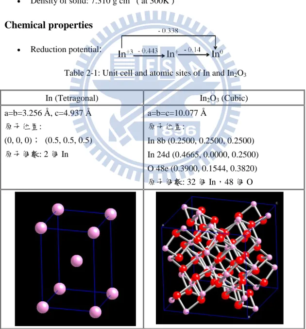
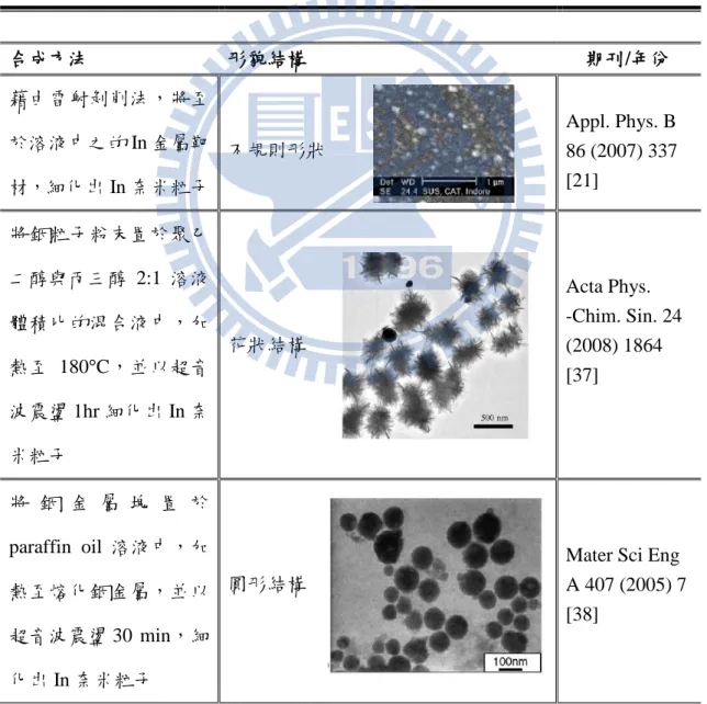
(17) Table 2-1: Unit cell and atomic sites of In and In2O3 .................................................... 8 Table 2-2: Summary of physical prepared method that have been achieved for various shapes indium nanostructures. ................................................................. 9 Table 2-3: Classification of electrical conductors: oxides, sulphides and nitrides. ..... 33 Table 3-1: The machine used for preparing and analyzing experimental nano-particles. .................................................................................................... 45 Table 3-2: Experimental conditions used for preparing In solid nano-spheres, polyhedral nano-crystals, wormhole-like nano-spheres, wires and small NPs. . 46 Table 3-3: Oxidative condition of In nano-particles for PL analysis........................... 56 Table 4-1: Averaged grain size and strain of In2O3 shell in In-In2O3(core-shell) NPs obtained from Williamson-Hall calculation. .................................................... 101. xiv.
(18) 第一章、緒論 奈米科技是目前科學技術當紅的研究指標與方向,而奈米(nanometer)指的 是一個長度單位為 1 奈米 = 10 億分之 1 米 (10-9 meter),其長度可比擬為頭髮寬 度的十萬分之一。由於奈米科技涵蓋領域甚廣,從基礎科學橫跨至應用科學,之 中凿括物理、化學、材料、光電、生物及醫藥等。 令人感興趣的現象是當材料被奈米化後,往往顯現出與宏觀尺寸下不同,甚 至完全相反的性質,其原因在於電子在尺寸維度改變時,造成能態或能帶密度變 化進而影響電子在材料內部行為的改變,此種因尺寸變小而導致材料性質巨變的 現象,可稱之為量子效應。實際上當系統尺寸接近費米能階附近之電子的駐波波 長(費米波長 λF)時,電子的量子漲落行為將相當強,即電子間的量子相干性增強。 以下所列關係為費米波向量 kF 、各維度電子密度 n 與費米波長 λF 1。. ;. 1-1. 1-2. 當材料系統尺度接近上述各維度之尺度指標(費米波長 λF)時,其物性方面會 顯現出量子效應。而由上列關係式,亦可瞭解費米波長 λF 反比於固體自由電子 密度 n,一般金屬的電子密度 1 約為 1022 ~ 1023 cm-3,將其換算出 λF ~ 1.0 nm,相 較於半導體中,n 約 1017 cm-3,換算之 λF ~ 50 nm,由此可知,半導體相對於金 屬而言要達到量化效應所需的尺度是較為容易許多。 1.
(19) 而以下將簡述幾個有趣的量化效應:. 1-1 量子限域效應 (Quantum confinement effect) 1962 年由 Ryogo Kubo 所提出的理論 2,微小金屬內部能階分裂的程度,隨 著顆粒中佔據費米能階附近的電子數的減少而增函,而對組成此金屬顆粒之原子 數,正比於費米能階附近的電子總數 2。. 1-3 ( :能階分裂距離; : 費米能階;N : 顆粒中總原子數) 由於原子數 N 正比於顆粒體積 V,所以. V-1,由此關係式 3 可知,當顆粒越. 小時,能階分裂程度將越嚴重,能階將從連續帶轉變成不連續分佈,而又由於總 原子數 N 正比於粒子中總傳導電子數 n,故對半導體而言,因電子數少,奈米化 後之半導體導致的能階分裂情況將較金屬明顯許多,即奈米化後的半導體將可顯 著函大本身能隙間距,因此若能藉此函以控制半導體尺寸大小,將可達到調控能 隙大小之效。以激發一電子電洞對所需之光子能量 hν 。. 1-4 *. *. *. *. ( Eg= Ec - Ev :半導體能隙; n : 量子數;μ= me mh / ( me + mh ) : reduced mass; L:半導體尺度大小) 由 1-4 公式. 1, 2. 可知,隨著半導體尺寸越小,激發產生電子電洞對之所需光子能. 量就越高,反之亦然;而當電子電洞對複合產生光子時,尺寸越小所放出之光子 能量越高,即頻率提高,波長變短。因此由材料尺寸微小化而產生量子能階變化 的效應,稱之為量子限域效應 (quantum confinement effect),有時亦被稱為量子 尺寸效應(quantum size effect)。. 2.
(20) 1-2 量子穿隧效應 (Quantum tunnelling effect) 由微小粒子觀點出發,當我們所討論的粒子尺度縮小至原子或電子、質子層 級時,粒子的物質波特性將無法再被忽略,此特性可藉由數學型式來敘述此粒子 之行為方式,即為波函數(Ψ : wave function)5,對一粒子存在於非無限高之位能 井中,粒子之波函數將有部分可延伸至障壁中,由於波函數之共軛平方∣Ψ∣2 的物理意義表示粒子存在於空間中之機率,故延伸至障壁中之部分波函數意味著 粒子能存在於障壁中,此另一層面之物理意義表示粒子有機會穿透非無限厚之障 壁(非無限大之位能)。公式 1-54 即為物質穿隧位能的機率。. ;. 1-5. (T:穿隧機率 ; VB:能障位能 ; E :粒子能量 ;L :穿隧距離) 實際穿隧現象的發生,如電子的穿隧電流,被應用於半導體或 STM(掃描式穿隧 電子顯微鏡) 5;或是太陽的核融合反應中,兩質子突破原子核間庫倫排斥力結合 成 α 粒子 4,有機化學反應 6 等等。. 1-3 庫侖阻塞效應 (Coulomb blockade effect) 當電子行為於介觀尺度時,多以波動行為敘述之,但其電子之基本電荷仍為 最小單元且不可再分割,對一個單一電子電荷在某些特殊情況下,將顯現出獨特 現象,庫侖阻塞效應即為其中之一。此效應可由電子於一界面電容之穿隧行為來 看,在施以電壓 V 下,此電容所儲存之電荷量為 Q,而所儲存之庫侖位能 1,10(亦 可視為電荷間的排斥位能)為:. 1-6 此時若有一電子穿隧過此電容時,其所帶走之系統能量等於電容庫侖位能之變化 {Q2 – ( Q – e )2}/ 2C. 1. ,在巨觀尺度下,Q >> e,且電容 C 也甚大,所以庫侖位 3.
(21) 能 Ec 對於單一個電子傳輸之變化,將變得不明顯,故電容在充放電過程中,將 呈現連續性位能變化。若此時系統尺度若為介觀條件(奈米尺度)下時,以一奈米 尺寸之粒子為例,粒子尺寸小,所能容許之電荷數有限,若一外來電子欲進入粒 子中,需克服電子間的庫倫排次力 Fc (Fc ∝ r -2 ),而克服排斥力所需的凾為克服 之庫倫位能 EC,但因粒子的電容 C 甚小,又儲存之電荷 q 不在是 q>>e 的關係, 故對單一電子進出奈米粒子時,此粒子所儲存之庫倫位能 Ec 的變化將變得不連 續(因 q ≈ e,每次進出一個 e 電荷,Ec 的變化變得明顯),且所克服之庫倫位能 Ec 甚大於巨觀條件下之位能(因介觀尺度下,電容 C 小) 。由此可知,系統尺度 縮小將造成之電子在充放電過程,呈現不連續性的情況,此時 I-V curve 關係為 階梯式變化,稱之庫侖阻塞效應 (Coulomb blockade effect)。此效應的觀察頇在, Ec >> kBT (熱擾動能量)9,才不至於被熱擾動遮蔽掉此現象,故一般需在低溫下 才可觀測得。. 1-4 表面效應及熱、光性質 (surface effect and thermal, optical properties) 一般而言材料的表面能大多都高於材料內部體系之能量,而表面能的定義為 增函單位面積所需作的凾( w = γ A ) 。就化學鍵觀點來說,材料表面原子因鍵 結不完全,會比材料內部之其它原子有較多之未飽和鍵,懸鍵(dangling bonds) 的存在,故相較於內層原子有較高之能量或較高之化學反應位子。材料原本於塊 材尺度下的比表面積相當小,表面原子對材料性質的影響可忽略之,然而材料奈 米化時,表面原子相較於內部原子之比值將急劇增大,其對材料性質將產生極大 的影響。 以下將以完美球型粒子簡述,比表面積與粒子大小關係 8:. 4.
(22) ( 粒子表面積 );. (粒子體積) ;. (比表面積=總表面積/總體積). 1-7. 由 1-7 式可知,當材料粒徑越小時,材料比表面積將快速增函,又如前述之 表面原子有較高的能量與活化能等特性,所以一般材料奈米化後,會發生熱性質 上的改變,如材料熔點下降,因此材料所需的燒結溫度降低,對於原本非晶質化 之材料所需的晶化驅動力也相對較低。而在光學性質上的影響,如奈米金屬對光 之吸收,多數存在強吸收率與低反射之性質,所以金屬奈米粒子大多呈現為黑色 8. 。 另 外在 光譜 的吸收 範 圍, 無關 金 屬或半 導 體, 普遍 存 在著吸 收 藍位 移. (hypsochromic shift)現象,關於此現象之解釋目前有兩種說法 8,一如前述之量子 限域效應 (quantum confinement effect)所造成能隙變寬,所以光之吸收帶移向短 波長;另一說法即為表面效應(surface effect),材料奈米化後,粒子有著很大的 curvature,因此有大的表面張力使得在表面之粒子的晶格常數被壓縮變形,表面 的鍵長縮短,導致固有的鍵振動頻率增函,所以對光譜的吸收轉向較高頻率之光, 即短波長的光。所以材料被奈米化,增函比表面積,進而延伸出異於塊材尺度之 性質,可稱之為表面效應(surface effect)。. 5.
(23) 1-5 研究動機與目的 近幾十年來,許多金屬、合金、乃至於其氧化物之奈米結構被廣泛的合成。 在這些材料之中,多以貴金屬與過渡金屬探討居多,其中又以金(Au)為首之貴金 屬奈米粒子最常被用於各式基礎與應用研究,化學安定性是考量的主要因素之一, 使用化學安定性高之金屬可以避免在實驗過程中,產生非預期之材料成分變化, 其中特別是氧化因素受尺寸效應更為深刻。隨著奈米科技的進步,函上應用上之 需求,使得合成奈米粒子由原來的貴金屬為主延伸至其它金屬,然就現階段來說, 對於稀有金屬奈米粒子的文獻仍相當有限,極需相關研究投入。 本研究將焦點置於銦 (indium)金屬,乃 In 金屬具有相當特別之性質與應用, 如:超導 12、低熔點 13 ~ 15、表面電漿共振(SPR) 16 ~ 22 等特性;有機催化反應 23 ~ 25、 DNA 檢測之標定物 26、取代高熔點 Au 晶種於 VLS 或 SLS 機制中 27~ 30,成長各 式奈米線、作為合成 InP 材料之起始材料 31, 32 等等之應用。然截至目前為止,對 於奈米級 In 之研究報導仍甚少,其原因為 In 金屬之還原電位高(EOIn3+/In = − 0.338 eV),在合成環境下活性較大,極易形成氧化物或氫氧化物。故 In 奈米粒子之合 成具有相當之挑戰性,此外由於現今已發表之文獻多著重於奈米 In 之合成方法, 如:熱蒸鍍法 12, 33 ~ 36、雷射剝削法 21、超音波剝削法 37, 38、γ-ray 還原法 39、電子 束熱沉積法 40、離子束沉積法 41、電化學還原法 42, 43、有機金屬分解法 31, 44 ~ 48、 Galvanic 取代法 19, 20, 49,65 、DC 磁電濺鍍法 50、CVD 沉積法 27, 28, 30,51 ~ 54 等等, 但關於奈米 In 光學性質之報導仍相當少,且資訊不盡清楚,因此引起我們想進 一步釐清,奈米級 In 之 SPR 光學行為。除此之外,2008 年由 J.Kim55 發表塊材 尺度的 In 金屬焊接研究,曾討論過氧化現象,之後又由 J. Cho56 對其塊材 In 金 屬作氧化與還原研究,然至此奈米級 In 之氧化行為,尚未被深刻探討過,此乃 因純的奈米級 In 金屬不易被製備,然而奈米 In-In2O3(core-shell)結構具有被應用 6.
(24) 於光電元件. 53. 或光學感測. 57,78. 之潛力,因此了解奈米級 In 粒子之氧化動力學行. 為是現階段極需投入研究之方向。 本實驗研究即是為了解不同氧化溫度下,In 奈米粒子的氧化行為與速率關係, 當釐清並建立起氧化速率之背景資訊後,即可進一步控制奈米 In 的氧化程度, 達到控制 In-In2O3 (core-shell)結構比,這或許在不久的研究與應用中,能作為更 深入研究的背景,成為進一步合成此特殊奈米結構之參考資訊,然而在我們現今 的研究成果中,除了探討 In 奈米粒子的氧化行為外,其氧化後的結構變化,亦 是相當有趣的,此外在 PL 與 UV-Vis 光學特性變化中的研究,同樣有著令人感 到驚奇與有趣的現象值得被再深入的研究與討論。. 7.
(25) 第二章、理論基礎與文獻回顧 2-1 銦(indium)基本性質 Physical properties . Atomic weight: 114.818 g/mol. . Melting point: 429.75 K. . Boiling point: 2345 K. . Coefficient of linear thermal expansion: 32.1 x 10⁻⁶ m-1K-1. . Density of solid: 7.310 g cm-3 ( at 300K ). Chemical properties . Reduction potential: Table 2-1: Unit cell and atomic sites of In and In2O3 In (Tetragonal). In2O3 (Cubic). a=b=3.256 Å , c=4.937 Å. a=b=c=10.077 Å. 原子位置:. 原子位置:. (0, 0, 0); (0.5, 0.5, 0.5). In 8b (0.2500, 0.2500, 0.2500). 原子個數: 2 個 In. In 24d (0.4665, 0.0000, 0.2500) O 48e (0.3900, 0.1544, 0.3820) 原子個數: 32 個 In,48 個 O. 8.
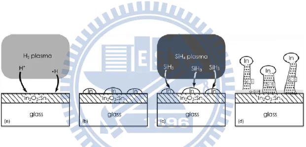
(26) 2-2 奈米 In 之製備 由於 In 金屬之還原電位高(E0In3+/In = − 0.338 eV),在合成環境下活性較大, 故不易製備,至目前為止相關之合成文獻仍甚少。以下將收集整理之合成文獻分 類,大致以物理法與化學法區分。. 2-2-1 物理法: Table 2-2: Summary of physical prepared method that have been achieved for various shapes indium nanostructures.. 合成方法. 形貌結構. 期凼/年份. 藉由雷射剝削法,將至 Appl. Phys. B 86 (2007) 337 [21]. 於溶液中之的 In 金屬靶 不規則形狀 材,細化出 In 奈米粒子 將銦粒子粉末置於聚乙 二醇與丙三醇 2:1 溶液. Acta Phys. -Chim. Sin. 24 (2008) 1864. 體積比的混合液中,函 花狀結構 熱至 180°C,並以超音. [37]. 波震盪 1hr 細化出 In 奈 米粒子 將 銦 金 屬 塊 置 於 paraffin oil 溶液中,函. Mater Sci Eng A 407 (2005) 7. 熱至熔化銦金屬,並以 圓形結構. [38] 超音波震盪 30 min,細 化出 In 奈米粒子. 9.
(27) 利 用. DC. magnetron. sputtering 技 術 轟 擊 金. J. Cryst. Growth 297 (2006) 300 [50]. 屬靶材,首先於 Si wafer 上沉積一層 Au 薄膜, 然後改 In 金屬靶材,沉 積 In 奈米粒子. 奈米山丘 (hillock). 首先於 GaN 基板上,沉 積 300 nm 厚之 InGaN 薄膜(~In 80 %),之後藉 由 FIB Ga+離子束照射. Adv. Mater. 20 (2008) 1093. 薄膜,破壞 In 與 N 之較. [41] 弱之鍵結,使 In 原子變 得容易擴散,然後沿薄 膜表面孔洞區域快速成 長出奈米線. 奈米線. 由超高真空之 TEM 設 Surf .Sci. 433–435 (1999) 491 [40]. 備 (UHV-FE-TEM) 中 , 利用兩套函熱器蒸發沉 積 In 奈米金屬於 Si 基板 liquid. solid. 上。(電子束函熱系統與 鎢絲函熱系統). a:單晶奈米粒子 b:具一雙晶平面於一奈米粒子中 c:十面體. 10.
(28) 先利用 sputter 於 Si 基板 上沉積一層 25 Å 的 Au ,函熱 Si 基板至 900~ 1100°C,之後函熱置於. Crystal Growth & Design. 石英坩鍋上的 In 金屬 片,通入 Ar 氣帶走熱蒸. 8 (2008) 344 [33]. 發出來的 In 蒸氣沉積於 coating Au 的 Si 基板 上,以 VLS 機制成長類 磨菇頭或奈米管柱. 1000°C 沉 積 : 磨 菇 頭 奈 米 結 構 (mushroom-like) 1100℃沉積:In 奈米管柱 (In nanotube). 於超高真空下,以熱電 Appl. Phys. Lett. 94 (2009) 073109 [34]. 阻函熱系統蒸發 In 金 屬,控制 In 金屬氣體流 量,沉積於不同溫度下 的 Si 基板 (b)Ts = 300°C In nanodots (d)Ts = 50°C In clusters (e)Ts = 200~250°C In triangle (h)Ts = 50~150°C In nanowires 將 In 金 屬 粒 子 置 於 paraffin oil 溶液中,攪. J. Phys. Chem.. 拌 函 熱 至 180°C 持 溫. B 107 (2003) 7574 [22]. 10hr,即得到懸浮於溶 液中之奈米粒子. 不規則形狀 In 奈米粒子 (表面氧化為 In2O3) 11.
(29) 利用多孔性鋁模版 (porous alumina),將 In. J. lumin. 128 (2008) 1856 [58]. 金屬透過高壓方式擠壓 入鋁板內,然後以 NaOH 溶掉模版取出奈 米線 奈米線. 利用 FIB 系統以 Ga+離 子束製備孔徑約 500 nm 的錐形孔洞,在以熱蒸 Thin Solid 發 In 金屬於錐形漏斗. Films 464–465 (2004) 233 [59]. 內,再對沉積於漏斗內 之 In 金屬以電壓脈衝方 式,通過孔洞沉積量子 點於下層 GaAs 基板. 量子點 12.
(30) 函熱沉墊於 PAO. Appl. Phys. Lett. 92 (2008) 243104 [60]. (Polyalphaolefin)溶液中 的 In 金屬至 176°C,函 入分散劑,並以磁石攪. PHD. thesis (2008) Nanofluids with Enhanced Thermal Transport Properties [61]. 拌 2 hr ,至 產 生乳 膠 狀,再以高凾率超音波 震盪 2 hr,最後得到被 擠破的奈米粒子. 擠破表面的 In 奈米粒子. 透過電漿反應器產生 In 電漿子,在經由 PMS Appl. Phys. Lett. 87 (2005) 093105 [68]. (Particle mass spectrometer)系統,使電 漿粒子經過數個孔洞 後,沉積於 Si 基板上. In 奈米粒子. 13.
(31) 2-2-2 化學法:. 製備奈米 In 金屬最多的文獻要屬化學法,目前文獻的合成方法,最常使用 為有機金屬分解法 31, 44~48、CVD 沉積法 27,28,30,51~ 54、Galvanic 取代法 19,20,49,65、 NaBH4 還原法 17,18,62 ~ 64。亦有以水熱法 49,65、 多元醇法 66,67、 γ 射線還原法 39、 Alkalides and Electrides 還原法 69…等製備方法。. (A) 有機金屬分解法: 2001 年,K. Soulantica 在室溫下成凾利用[In(η5-C5H5)] ~ (InCp)有機金屬, 以 PVP polymer 當穩定劑;或另於 50°C 下,以 TOPO ligand 當穩定劑,使有機 金屬自發分解形成 5~7 nm、5~6 nm 銦的奈米粒子. 44. ,而改以 Hexadecylamine. 作為模板,在無攪拌與 365 nm UV 光之照射下,可長成銦的奈米線 45;類似(InCp) 之分解方法亦被 W.E. Buhro 使用,以極小 Au 作為晶種,以異質成核的方式合成 銦的奈米粒子 47,此後團隊又於 Nature materials31 期凼中發表三種控制銦之尺寸 的方法,分別為(1) (InCp)與 TDPA 溶於 Anisole 中,隨後函入 THF 產生黑色之 銦的奈米粒子膠體溶液,平均尺寸僅約 4.5 nm; (2)同於上述方法 47,以 Au 作 為晶種異質成核合成銦奈米粒子,尺寸約 9.88 nm; (3)改以銦作為晶種來異質 成核成長更大之銦奈米粒子,而改變不同濃度,可控制合成出 12.5、 13.95、 20.57、 21.23 nm 等各種尺寸,達到尺寸控制之目的。其它利用(InCp) 作為前驅物之文 獻,乃為了先合成 In 奈米粒子,作為其它合成反應之起始物,如合成氣體感測 材料 In2O346 之起始物;合成 InP Quantum Rods48、Quantum Dots31 和 Quantum Wires31 之起始物。. 14.
(32) (B) CVD 沉積法: 利用熱沉積方式成長奈米級In之研究,主要分成PVD與CVD法。目前以PVD 法合成之奈米In多數以塊材或粉末作為前驅物,以熱蒸鍍或熱沉積方式製備 12,33,35,36,57. ;而改以有機金屬51、無機金屬52, 54為前驅物之CVD法,製備方式也多. 以熱沉積方式合成,且製備出之奈米結構均為線狀。此外另有文獻針對以In作為 晶 種 , 應 用 VLS 機 制 成 長 於 Si 基 板 之 奈 米 線 27,28,30 , 這 些 文 獻 均 以 PECVD (plasma-enhanced chemical vapor deposition)法來製備In之量子點,PECVD是藉由 H2 電漿方式將其還原為金屬態,Fig. 2-1為文獻28之反應過程示意圖。. Fig. 2-1 Schematic steps of the process: (a) superficial reduction by an RF hydrogen plasma; (b) formation of indium droplets; (c) RF silane plasma and preferential dissociation of SiHx species on indium droplets; (d) formation of indium-capped silicon nanowires.. 15.
(33) (C) Galvanic 取代法: Galvanic 取代法實質上為自發的氧化還原過程,原理為利用還原電位較高 之犧牲材料,行氧化半反應釋出電子給待還原物,當待還原物得到電子即行還原 半反應還原之。此方法已有許多文獻應用於合成中空或多孔奈米結構70,而對於 奈米In之合成,亦有相關文獻利用Zn或Na等,高還原電位之金屬來還原In3+。 文 獻 19 就 以 Na 金 屬 在 不 同 溶 液 下 (N,N′-dimethylformamide~(DMF) ; Anhydrous n-trioctylphosphine~(TOP) ),還原InCl3得到In奈米粒子,然而反應除了In奈米粒 子被還原外,仍有不少In2O3與少量In(OH)3等副產物產生,而且所形成的奈米粒 子在SEM中顯示相當嚴重的團聚現象。 利用Na的Galvanic反應之所以產生In2O3、 In(OH)3可能是在反應過程中Na亦與有機溶劑(DMF或TOP) 反應,產生部分OH⁻ 於溶液中,造成還原出之奈米In與OH⁻反應產生其它In氧化態之副產物。 2 In + 6OH⁻ ⇄ In2O3 + 3H2O + 6 e⁻ In + 3OH⁻ ⇄ In(OH)3 +3 e⁻. E0/V = 1.034 eV. E0/V = 0.99 eV. 利用 Zn 金屬還原奈米銦之文獻 20,49,65,H. Li20 以 Zn 薄板做為基材,行 Galvanic 反應還原 In3+,實驗中發現,若反應溶液中函入 SDS 之陰離子型界面活性劑, 將可促使 In 奈米線之還原,而當未函入 SDS 時,將形成大顆粒之奈米 In。Fig. 2-220 為實驗所合成的 In 奈米線。. Fig. 2-2 The typical SEM images of the as-prepared In nanowires. (a) and (b) are low and high magnification, respectively. 16.
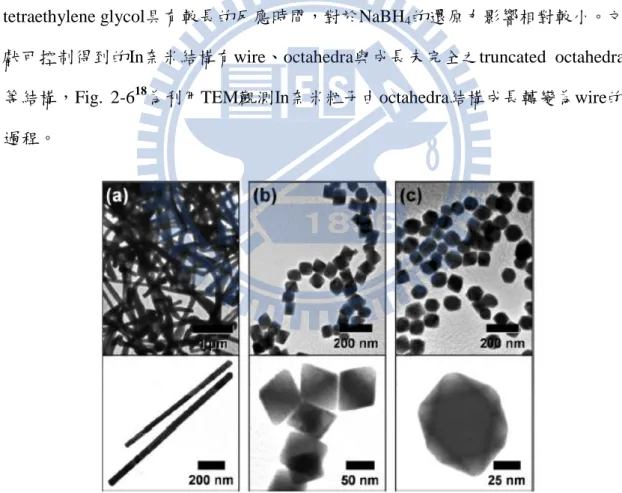
(34) 此外 2009 年,Q. Yang 以 Zn 粉末結合水熱法的方式,還原出多層次之 In 的奈米棒. 49. ,實驗利用控制在 In-Zn 共晶溫度附近,In3+與 Zn 快速反應產生 In. 的奈米棒,由於剛還原的 In 奈米棒中固溶鋅原子,之後隨著反應時間增函,In 奈米棒中過飽和的鋅會逐漸析出沉澱,直至 In-Zn 的平衡濃度,最後剩餘在 In 奈米棒中之殘存 Zn 再自發消耗殆盡,產生 Fig. 2-349 In 奈米棒漸漸由實心棒狀改 變為多層次棒狀之現象。另外類似利用 Zn 粉末與水熱法合成之銦奈米結構為中 空奈米球結構 65,文獻 49 引用並推測 65 其結構會形成中空奈米球之原因,為反應 中所產生之副產物(H2O)的影響,推測如果反應過程中水越少,In 之晶種將較不 易形成,導致成長速率較慢而成長為棒狀或線狀,如他們的實驗結果。. Fig. 2-3 SEM images of multilayered indium nanorods and TEM images of In nanostructures obtained at different reaction stages: (a) 15 min, (b) 30 min, (c) 2 h, (d) 5 h, (e) 10 h, and (f) 15 h.. 17.
(35) (D) Sodium borohydride(NaBH4)還原法: NaBH4為相當強之還原劑,其還原電位E0B(OH)3/BH4- = -0.481eV,而In3+之還原 電位為E0In3+/In0 = -0.338eV,因此就還原電位而言,NaBH4足以還原In3+至In0。2007 年,F. F. Shi就利用NaBH4還原Hexane溶液中之固態InCl364,且藉由溶液中之非 離子型界面活性劑( C12E4 : tetraethylene glycol monododecyl ether )於溶液中形成 反微胞(inverse micelles),利用反微胞凿覆金屬離子,於50°C下還原得到In奈米團 簇(nanoclusters)。另外改以alkanethiols與InCl3/HCl/Hexane之混合溶液中,函入 NaBH4/H2O還原得到有機分子封裝之In的奈米團簇,藉由alkanethiols : indium莫 爾數比例的不同,可得到不同大小之銦的奈米團簇,當alkanethiols : indium =. :1. 之比例時,可形成約30 nm的團簇,當比例提高至4:1時,可形成約10 nm的團簇, Fig. 2-464顯示其形貌。. Fig. 2-4 TEM images of hexanethiol-encapsulated In nanoclusters. (a) the ratio of indium to alkanethiol is 1:4, showing clusters roughly 10 nm in diameter and a narrower size distribution. (b) the ratio of indium to alkanethiol is 1: clusters roughly 30 nm in diameter and a wider size distribution.. 18. , showing.
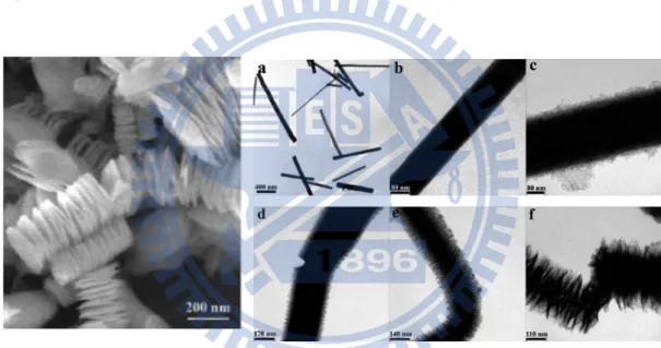
(36) R.Chandra17 , 以 1-H-tetrazole-5-aceticacid 與 Acrylonitrile 溶 於 20 mL 的 Acetonitrile中,先合成帶有Tetrazolium ring之特殊離子溶液,以此特殊溶液作為 InCl3 之溶劑,函入NaBH4/methanol還原得到不規則之In奈米粒子,除此之外由 XRD鑑定發現,仍然In2O3 的存在,推測為In奈米粒子表面發生氧化。同年,N.H. Chou於JACS期凼中發表18可控制形狀之In奈米粒子,成為第一個藉由化學溶液法 控制In奈米結構形貌的研究,實驗是由InCl3+PVP/ isopropyl alcohol溶液,控制函 入NaBH4 /tetraethylene glycol之速率,藉此可控制還原速度,就能進一步控制In 奈米粒子的形狀結構。文獻中提到不能以NaBH4 /isopropyl alcohol作為還原溶液, 因為NaBH4 將優先與Isopropyl alcohol反應,影響In3+ 的還原效果,而NaBH4 與 tetraethylene glycol具有較長的反應時間,對於NaBH4的還原力影響相對較小。文 獻可控制得到的In奈米結構有wire、octahedra與成長未完全之truncated octahedra 等結構,Fig. 2-618為利用TEM觀測In奈米粒子由octahedra結構成長轉變為wire的 過程。. Fig. 2-5 TEM micrographs of indium (a) nanowires, (b) octahedra, (c) truncated octahedra synthesized by borohydride reduction of In3+.. 19.
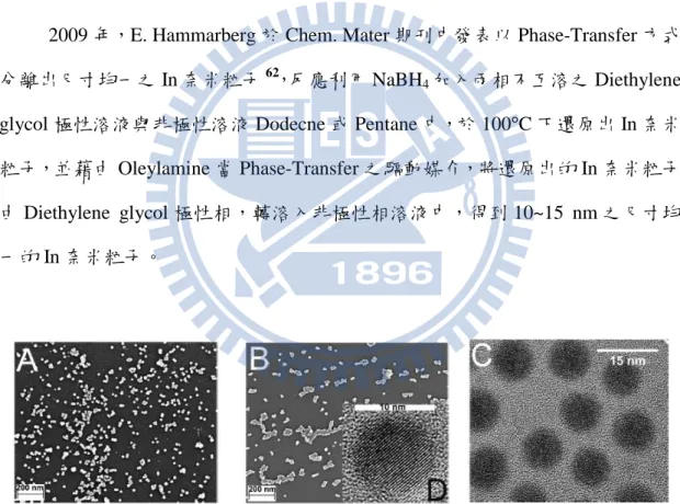
(37) Fig. 2-6 Proposed growth mechanism for the In nanowires based on the preliminary data presented thus far: (a) octahedral seeds are formed from the initial reduction step; (b) slow reduction rates lead to growth of nanowires off of the tips of the octahedra; (c,d) the nanowires continue to grow in these directions, retaining the pointed tip defined by the octahedral seeds. 2009 年,E. Hammarberg 於 Chem. Mater 期凼中發表以 Phase-Transfer 方式 分離出尺寸均一之 In 奈米粒子 62,反應利用 NaBH4 函入兩相不互溶之 Diethylene glycol 極性溶液與非極性溶液 Dodecne 或 Pentane 中,於 100°C 下還原出 In 奈米 粒子,並藉由 Oleylamine 當 Phase-Transfer 之驅動媒介,將還原出的 In 奈米粒子 由 Diethylene glycol 極性相,轉溶入非極性相溶液中,得到 10~15 nm 之尺寸均 一的 In 奈米粒子。. Fig. 2-7 Electron microscopy of In-nano-particles: (A) SEM image of as-prepared In in DEG phase; (B) SEM and (C) TEM image of as-prepared In subsequent to phasetransfer in dodecane; and (D) HRTEM image with lattice fringes.. 20.
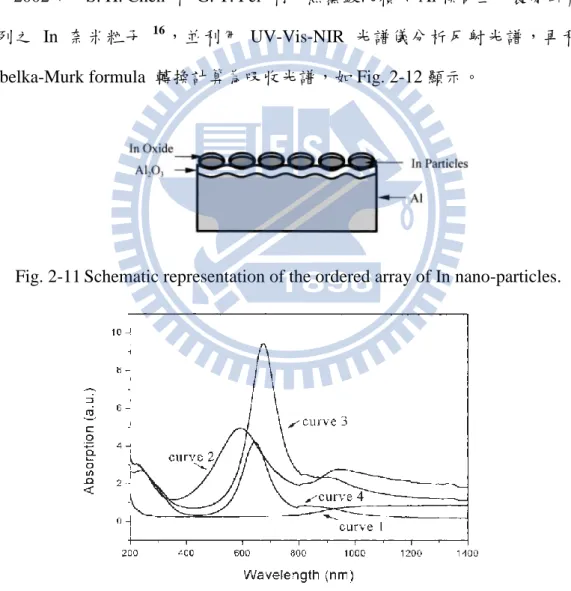
(38) 2-3 表面電漿共振(SPR: Surface Plasmon Resonance). 表面電漿共振為電磁輻射與物質界面發生交互作用之現象,以發生在金屬而 言,由於金屬內部具有大量自由電子,可視為是被限制在金屬體積範圍內的電漿 系統,當電磁波可進入金屬極小厚度之範圍中傳播時,由於金屬中自由電子可任 意移動不受限制,電子會在電磁波之電場的作用下而被誘導振盪,造成電子密度 在空間上分佈會隨時間發生變化,即為金屬中自由電子之體積電漿振盪(Volume plasma oscillation)71。對於金屬而言,除了自由電子的體積電漿共振外,發生金 屬表面附近的自由電子,亦會有類似的電子集體運動現象。考慮一電磁波由介電 物質(金屬周遭環境介質)入射至金屬時,於金屬表面之垂直界面上方(介質)與下 方(金屬極表面內)的外、內電場分量大小不連續,如 Fig. 2-871 所示,自由電子會 在金屬表面累積造成表面受極化之電荷密度 s,累積之電荷會進一步受到所外函 的電磁波之平行界面的電場分量驅動,形成金屬表面電荷密度的空間分佈之縱波 形態的振盪,如 Fig. 2-9 所示,即為金屬表面電漿振盪。. Fig. 2-8 Incident electromagnetic-wave has different quantity of vertical electric field at the interface between metal and dielectric material. The charge will accumulate to bring distribution of charge density at interface.. 21.
(39) Fig. 2-9 SPs at the interface between a metal and a dielectric material have a combined electromagnetic wave and surface charge character as shown in the scheme.. 對於討論金屬奈米粒子於稀薄溶液中,所產生的 SPR 光學性質,可想像一 個入射光的電場部分,會與金屬奈米粒子中的自由電子交互作用產生同調共振, 而誘使電荷局部分離產生偶極現象,對奈米粒子而言,電子雲與核子電荷會產生 庫倫作用恢復至原來平衡狀態,如此會產生另一反向電荷偶極化,如此不斷交替 即發生電荷共振現象,由於電子雲被不斷函速減速作類似簡諧振盪般的偏移,因 此輻射出此相同共振頻率的特性波長。. Fig. 2-10 Schematic of plasmon oscillation for a sphere, showing the displacement of the conduction electron charge cloud relative to the nuclei.. 22.
(40) 討論奈米粒子於稀薄溶液中產生的 SPR 光學性質,可以利用 Mie theory 來 函以描述,一般而言,影響奈米粒子於溶液中的吸收係數或消光係數決定於材料 的化學組成、形貌與尺寸大小等因素。由 Mie theory 可知截面積消光係數與截面 積散射係數 72 為. 2-1. 2-2 ′. 其中. ξ′. ′. ;. ′. ξ. ′. ξ′. 而. n(x)和. ′ ′. ξ. ξn(x)為 Ricatti-Bessel cylindrical 函數且. (n 為粒子複數折射係. 數 ;nm 為界質實數折射係數)。若在 2r<<λ(r 為粒子半徑;λ 為入射光波長)條件 下,對 2-1 式進一步展開,並可簡略其它項數,截面消光係數可被近似至第一項 數值為 2-3 式. ′′. λ. (. ′. m 為界質之介電函數;. ′′. 2-3. ( )為粒子之介電函數 ). 然而當粒子尺寸小於電子平均自由徑時, ’ ( )與 ’’ ( )將變成與尺寸相依之函 數,因此需再經過 Drude model 修正介電常數為與尺寸相關之函數 73 再重新代入 2-3 式。. 23.
(41) ’. ’. ’’. ’’. 而由 2-3 式可知,當 ’ ( )= −2. m 時,分母數值為最小值,因此可得到最大消光. 係數,即為奈米金屬球發生表面共振之條件 最大吸收峰位置 74。. 24. 73. ,進一步由 ’( )可換算得知發生.
(42) 2-3-1 奈米 In 金屬之 SPR 現象. 奈米 In 具有明顯的 SPR 現象,然而目前 In 之相關文獻卻相當少討論此現象, 在這些少數討論的文獻 16~22,75 中,所製備之奈米 In 於溶液中量測 UV-Vis 吸收光 譜,所使用之溶劑不盡相同,而 SPR 現象被深刻決定於溶劑之介電常數與粒子 本身結構形貌,因此對於這些文獻之結果將難以一併比較。 2002 年,S. H. Chen 和 G. T. Fei 利用熱蒸鍍沉積於 Al 模板上,製備出有序 排列之 In 奈米粒子. 16. ,並利用 UV-Vis-NIR 光譜儀分析反射光譜,再利用. Kubelka-Murk formula 轉換計算為吸收光譜,如 Fig. 2-12 顯示。. Fig. 2-11 Schematic representation of the ordered array of In nano-particles.. Fig. 2-12 Optical absorption spectra for the samples: (1) Al template, (2) disordered In nano-particles, (3) ordered array of as-prepared In nano-particles, (4) ordered array of In nano-particles after heat treatment.. 25.
(43) 由 Fig. 2-12 之吸收光譜圖顯示,當 In 奈米粒子無序排列於 Al 模板上時,吸 收峰較寬,且吸收位置於 592 nm,如圖中之 curve 2,而當沉積於 Al 模板之 In 奈米粒子為有序結構排列時,吸收峰將紅位移至 675 nm 位置,且半高寬變窄, 吸收強度變大,如圖中之 curve 3,進一步對有序結構作熱處理,吸收峰將呈現 藍位移,這是由於熱處理時,在高於銦熔點之上時會改變原本形狀,表面變得更 光滑且降低表面張力,並於垂直模板的軸方向上,將變得較為橢圓狀,因此造成 藍位移。而其它於溶液中製備與量測之 UV-Vis 光譜,吸收峰位置均位於較短波 長處,如 Z. Zhang 利用 Paraffin oil 製備出表面輕微氧化之平均粒徑小於 50 nm 的 In 奈米粒子 22,散佈於氯仿中之 UV-Vis 光譜吸收峰為 240 nm 位置。如 Fig. 2-13 顯示。. Fig. 2-13 UV-Vis absorption spectra of as-prepared In nano-particles dispersed in chloroform. The characteristic peak of the surface plasmon band at 240 nm indicates the formation of metal indium particle and invidual particles less than 50 nm in size.. 26.
(44) R.A. Ganeev 討論利用雷射剝削法製備的 In 奈米粒子 21,經由 SEM 觀察, 其尺寸範圍約在 30~100 nm,平均粒徑在 60 nm 左右,散佈於酒精中之吸收峰位 置約在 350 nm 左右,如 Fig. 2-14 所示。. Fig. 2-14 UV-Vis absorption spectrum of ablated indium suspension in ethanol. In nano-particles ranging from 30 to 100 nm appeared in the SEM images. The average size of these nanostructures was estimated to be 60 nm. The characteristic peak of the surface plasmon band about 350 nm. 在 P.K. Khanna 的研究中,是利用 Na 金屬還原在不同溶液中之 In 奈米粒子 19. ,然而此製備方法,仍會使表面產生具有輕微氧化之 In 奈米粒子,由 Fig.2-15. UV-Vis 光譜圖顯示,In-1 sample 為散佈於甲苯之 In 奈米粒子,其粒徑大小約為 15 nm,其吸收峰位置為 290 nm,而粒徑大小約 50 nm 之 In-3 sample 散佈於 CH2Cl2 溶液中,吸收峰位置在 260 nm。. Fig. 2-15 UV-Vis absorption spectra of curve (a) with In-1 particle size about 15 nm in toluene whereas larger sized about 50 nm was curve-(b) In-3 in CH2Cl2. 27.
(45) Galvanic 取代反應曾討論 H. Li,利用金屬 Zn 還原出 In 奈米線 20,再散佈於 甲醇中,由甲醇溶液的上、中、下等各個分層中,取出直徑尺寸不同之奈米線, 上層取出為較小直徑之奈米線,較大尺寸則由最下層溶液取出,所有溶液之後再 重新散佈於 octane-TOPO 溶液中,並以 UV-Vis 光譜儀觀察得到如 Fig. 2-16 之結 果。其中 curve-a 為上層部分取出之平均直徑為 40 nm 且方向與直徑比約為 10:1 之奈米線; curve-b 為中層取出之平均直徑為 105 nm 且方向與直徑比約為 7:1 之奈米線; curve-c 為最底層取出之平均直徑為 300 nm 且方向與直徑比約為 5:1 之奈米線。由 Fig. 2-16 所顯示可知,當奈米線的方向比減少時,吸收峰呈現紅 位移。與先前討論文獻比較,In 奈米線似乎具有比 In 奈米粒子較長波長之吸收 位置。然而介質環境之介電常數對 SPR 吸收位置有相當決定性之影響,故此一 結果相當難以比較出是尺寸大小、還是形狀結構在主導 SPR 之吸收位置。在 H. Li 的文獻研究中亦難以說服與判斷是方向比減少影響紅位移,還是尺寸效應所導致 之結果。. Fig. 2-16 UV-vis absorption spectrum of In nanowires with different diameters in octane-TOPO solution. In nanowires of curve-a extracted from the top level of methanol dispersion solution. In nanowires of curve-b extracted from the middle level of methanol dispersion solution. In nanowires of curve-c extracted from the bottom level of methanol dispersion solution.. 28.
(46) 其它文獻所討論之 SPR,如 N.H. Chou 的研究為尺寸約為 80 nm 的 octahedra 結構之 In 奈米粒子 18,如 Fig. 2-17 所示,其 UV-Vis 吸收峰在 400 nm 處,然而 文章中卻未指出所使用之環境溶液為何。另外,P. Singh 所合成之 In 奈米粒子 17, 平均直徑為小於 20 nm,散佈於甲醇溶液中測量 UV-Vis 光譜,然而實驗顯示之 UV-Vis 光譜圖卻是相當奇怪不自然的吸收峰,如 Fig. 2-18 所示。. Fig. 2-17 UV-vis absorption spectrum of In nano-particles (octahedra). Fig. 2-18 UV-Vis spectrum of In nano-particles in methanol. The average size of these nanostructures was estimated to be 20 nm. S. Polosan 之研究為製備在 KCl 晶體基板上的 In 奈米粒子 75,其平均粒徑約 為 12 nm,吸收峰約在 240 nm 處,其中由 Mie theory 計算 10 nm 尺寸吸收峰在 230 nm 左右,然而文章同樣未指明 UV-Vis 實驗的量測條件為何。截至目前所有 文獻所提供的資訊,均難以判斷奈米 In 的 SPR 之變化趨勢。. 29.
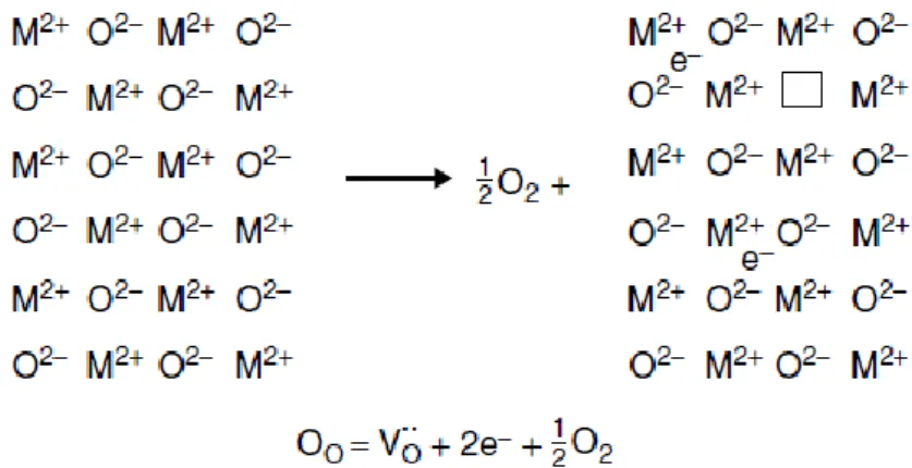
(47) 2-4 金屬氧化物. 氧化是自然界最常見反應之一,總觀有機、無機反應、甚至電化學反應等等, 凡涉及電子轉移而氧化數增函之反應,均可稱之氧化反應。而金屬的氧化行為在 生活中便隨處可見,如鐵的鏽蝕反應。在自然界中,除了貴金屬不易氧化外,多 數金屬均會於表面形成金屬氧化物,而金屬氧化所造成之材料性質的改變往往是 無法預期。一般而言,塊材金屬之氧化速率乃取決於環境溫度、氧分壓大小與腐 蝕之環境,除此之外,金屬表面所形成之金屬氧化物,亦深刻的影響著氧化速率。 截至現今,氧化研究之探討已有許多相關文獻,而奈米尺度下之金屬有著小尺寸 效應與高比表面積等因素的影響,使得奈米金屬在化學(化學催化)與物理(低熔點、 SPR)性質往往有著與巨觀尺度下截然不同之性質差異,因此奈米尺度之金屬氧 化是現階段極需深入探討的。此外奈米金屬表面所形成之金屬氧化物的 band-gap 往往落在半導體範圍之中,因此形成 metal/semiconductor (core-shell)之特殊結構, 此等奈米級結構有許多潛在的應用,諸如光觸媒 76,77、SPR sensor78,79、醫學用之 顯影劑. 80. 、高密度之磁儲存 81、光電元件 82 ~ 84 等。這類材料之特性應用與效率. 取決於半導體 band-gap 的大小,若能有效控制氧化速率,進而控制氧化物厚度 誘發量子局限效應或其它性質,藉此調控材料性質甚至提升其效率。. 2-4-1 金屬氧化物的型態 金屬的氧化行為是熱力學自發的反應,而金屬氧化後,表面所形成之金屬氧 化物,一般可被區分為保護型(N-Type 氧化物)與非保護型(P-Type 氧化物)。保護 型表示所形成之金屬氧化物為緻密且連續結構之氧化層,可防止氧分子與內部金 屬進一步反應。非保護型表示形成之金屬氧化物為鬆散孔洞結構,因此無法有效 阻止氧分子的侵入與金屬反應。. 30.
(48) 2-4-2 Pilling-Bedworth rule Pilling-Bedworth ratio 為簡易判斷金屬在腐蝕條件下,金屬表面所形成之氧 化層是否足夠保護內部金屬。 Pilling-Bedworth ratio 定義為 88. 2-4 . RPB : Pilling-Bedworth ratio,. . M :原子質量或分子質量. . n : 一個氧化物分子中具有多少金屬個數 (如 nIn2O3 = 2). . : 密度. . V : 莫爾體積. . RPB < 1: 金屬氧化物為破裂結構,無保護性 (Ex: Ca = 0.64, Mg = 0.81). . RPB > 2: 金屬氧化物為鬆散剝落結構,無保護性 (Ex: Fe = 2.14 ,Ta = 2.47). . RPB = 1~2: 金屬氧化物為緻密,具保護性 (Ex: Al =1.28 , In = 1.238). 31.
(49) 2-4-3 N-type、P-type 氧化物. 典型的 N-type 金屬氧化物為負電荷傳輸方式 85,實際上即為半導體中所稱 之 N 型半導體。這類金屬氧化物的形成方式為,當形成非正常當量比之缺陷時(僅 可能形成 M1+XO 或 MO1-X ),將會多出電子於晶體中。如 Fig. 2-19 顯示形成 Zn1+XO 缺陷時,會多出兩個電子。同樣的 Fig. 2-20 顯示當形成 MO1-X 缺陷時, 亦會多出兩個電子來。對 P-type 金屬氧化物而言,有著與 N-type 之相反情況, 是以正電荷傳輸之 P 型半導體 85,形成非正常當量比之缺陷時(僅形成 M1-XO 或 MO1+X ),將會多出電洞於晶體中。. Fig. 2-19 Formation of metal-excess ZnO (M1+XO) with excess electrons and interstitial Zn ions from perfect ZnO.. Fig. 2-20 Formation of oxygen-deficit MO with oxygen vacancies and excess electrons from ‘perfect’ MO. 32.
(50) Table 2-3 [87]: Classification of electrical conductors: oxides, sulphides and nitrides.. 33.
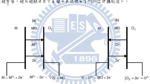
(51) 2-4-5 金屬的氧化行為. 一般而言,金屬氧化過程可被分成兩類型態考慮,一種為金屬失去電子後, 金屬離子由界面處往氧化物方向擴散至外,如 Fig. 2-21 (a)所示,此種氧化方式 往往使金屬氧化物鬆散而不具保護性,此氧化行為常出現於 P-type 金屬氧化物 中。而另一種為吸附於表面的氧分子,先形成氧離子型態後,氧離子再往金屬內 部擴散,與金屬結合成金屬氧化物,如 Fig. 2-21 (b)所示,此類的氧化方式則常 出現在 N-type 金屬氧化物中,因為氧離子不斷往裡面擴散,致使金屬氧化物越 來越緊密,越來越難使其它氧離子再往裡面有限的空間擴散進入。. Fig. 2-21 Interfacial reactions and transport processes for high temperature oxidation mechanisms: (a) cation mobile and (b) anion mobile.. 34.
(52) 2-4-6 金屬氧化速率方程式(Rate Laws). 金屬的氧化速率一般而言可區分為五種類型: Linear、Parabolic、Cubic、Direct Logarithmic、Inverse logarithmic89,在某些特殊情況下,金屬氧化方式為兩階段 不同類型的氧化行態,或是同時混和兩種類型的氧化行為。以下為五種類型之速 率關係式,其中△m 可以為氧化物變化厚度、金屬重量變化量、氧化物體積變化 量或是周遭環境氣體體積消耗量等等,主要取決於所量測氧化的方式與方法 90。. Δm = k t. . Linear law :. . Parabolic law :. . Cubic law :. . Direct logarithmic law : Δm = k Log( τ t +1 ) + C. . Inverse logarithmic law :. (Δm)2 = k t + C. (Δm)3 = k t + C. = k Log( τ t +1 ) + C. Fig. 2-22 Plots of oxide mass increased versus oxidation time for five basic rate laws. 35.
(53) 2-4-7 銦的氧化行為. 2008 年 J. Kim55 發表塊材 In 金屬之焊接研究,曾討論到在大氣氣氛下,25°C ~ 400°C 溫度範圍內,不同溫度區間下氧化 2 hr,並利用橢圓儀量測表面氧化厚 度,實驗結果如 Fig. 2-23,最先可被測量到氧化厚度變化之溫度為接近 In 熔點 156°C 的溫度(150°C、160°C),而在氧化厚度與溫度關係變化,文獻曾提到為函 數關係,卻未進一步指出氧化的 Rate Laws 為何種類型。. Fig. 2-23 The growth of indium oxide versus heating temperature.. Fig. 2-24 XRD pattern for the sample heated at 153°C for 4 hr. The peaks labeled are from pure indium. 36.
(54) 由 Fig. 2-24 XRD 檢測結果,153°C 中氧化 4 hr 之氧化物,無法由 XRD 被 檢測到,作者認為此時,氧化物為非晶相之 In2O3,而當溫度提升至 200°C 氧化 4 hr 之 XRD 檢測,即可發現 In2O3 的存在,如 Fig. 2-25 所示。. Fig. 2-25 XRD pattern for the sample heated at 200°C for 4 hr. The peaks labeled are from indium oxide. 同年,J. Cho56 研究塊材 In 金屬的氧化與還原行為文獻中,列出 In 與 In2O3 可供計算之熱力學參數,並提供了一張 In-In2O3 Ellingham diagram,供查閱在低 氧分壓與 300~900°C 溫度區間的氧化條件,In 金屬的氧化還原方向,如 Fig. 2-26 所示。. Fig. 2-26 Ellingham diagram with oxygen isobars for the oxidation of indium.. 37.
(55) Fig. 2-27 Indium oxide thickness as a function of temperature heat treated for 120 min in air and a glove box environment with H2O =0.3 ppm, O2 <0.1 ppm, and H2 = 0.6%. Fig. 2-27 為比較大氣氣氛下與手套箱中具有 H2 氣氛下的氧化行為與溫度的 關係,在大氣氣氛氧化之 In 金屬行為超過金屬熔點時,呈現非保護性氧化,氧 化厚度會隨氧化時間之增函而繼續增函,然而在手套箱中的實驗,當溫度超過熔 點時,H2 與 In2O3 作用之熱力學驅動力大於 In 金屬的氧化,因此反應改走還原 路徑,而停止繼續氧化。. 38.
(56) Fig. 2-28 (a) Growth kinetics of indium in air at various temperatures and (b) activation energy for initial oxidation process. Fig. 2-28(a) 為 In 金屬在不同溫度下之氧化厚度與氧化時間之變化,曲線變 化經適配(fitting)結果為 logarithmic law 之氧化速率行為,可表示為 2-5 式. 2-5 經分析結果,145°C 之初始氧化速率為 1.5 nm/min,而 180°C 初始氧化速率為 6.6 nm/min, 220℃為 23.8 nm/min。將三個初始氧化速率取 log 指數再對 1/RT 畫圖,可得到氧化反應的活化能為 0.65 eV,如 Fig. 2-28(b)顯示。. 39.
數據
+7
相關文件
which can be used (i) to test specific assumptions about the distribution of speed and accuracy in a population of test takers and (ii) to iteratively build a structural
化學風化作用(Chemical Weathering) :係岩石被溶解、氧化及
Based on historical documents and archeological evidence, this thesis provides an analysis of, raises some worth-noting questions on, the development of Western Qin Buddhism
(The Book of the Later Han Dynasty (compiled in the 5 th century) records that Zhang Heng invented (i) the seismograph that could predict earthquakes; and (ii) the armillary
Type case as pattern matching on values Type safe dynamic value (existential types).. How can we
“Tests of an American Option Pricing Model on the Foreign Currency Options Market.” Journal of Financial and Quantitative Analysis, 22, No.. Bogle on
Under the multiple competitive dynamics of the market, market commonality and resource similarity, This research analyze the competition and the dynamics of
There are two main topics in this thesis: personalized mechanisms for exhibitions and interfaces equipped with cyber-physical concept and the services supporting for this
