國 立 交 通 大 學
電子工程學系 電子研究所碩士班
碩 士 論 文
電漿氣相輔助沉積氮化矽覆蓋層之形變 N 型金氧
半場效電晶體之電流增強方法與可靠度之研究
A Study of Drive Current Enhancement Methods
and Relability Issues of Strained NMOSFETS
with PECVD SiN Capping Layer
研 究 生:詹凱翔
指導教授:林鴻志 博士
黃調元 博士
電漿氣相輔助沉積氮化矽覆蓋層之形變 N 型金氧
半場效電晶體之電流增強方法與可靠度之研究
A Study of Drive Current Enhancement Methods
and Relability Issues of Strained NMOSFETS
with PECVD SiN Capping Layer
研 究 生
:
詹凱翔 Student
:Kai-Hsiang Chan
指導教授 : 黃調元 博士 Advisors :Dr. Tiao-Yuan Huang
林鴻志 博士
Dr. Horng-Chih Lin
國 立 交 通 大 學
電子工程學系 電子研究所碩士班
碩 士 論 文
A Thesis
Submitted to Department of Electronics Engineering & Institute of Electronics College of Electrical and Computer Engineering
National Chiao-Tung University in Partial Fulfillment of the Requirements
for the Degree of Master of Science
in
Electronic Engineering June 2007
Hsinchu, Taiwan, Republic of China
具電漿氣相輔助沉積氮化矽覆蓋層之形變 N 型金
氧半場效電晶體電流增強方法與可靠度研究
研究生 : 詹凱翔 指導教授 : 林鴻志 博士
黃調元 博士
國立交通大學
電子工程學系 電子研究所碩士班
摘要
在本論文中,我們主要探討在 N 型金氧半場效電晶體中,利用電漿氣相輔助 沉積(PECVD)氮化矽覆蓋層及其相關沉積製程參數對元件特性與熱載子退化效應 的影響。我們在沉積氮化矽覆蓋層時,固定矽甲烷(SiH4)與氨(NH3)的流量,而調 整氮(N2)流量,使所沉積的氮化矽覆蓋層舒張應力增加,來造成元件通道的形變, 進而增進元件載子遷移率。在實驗中,我們也利用一不同特性的電漿氣相輔助沉 積系統,來沉積具壓縮應力的氮化矽覆蓋層,並證實了元件在舒張的應力下可得 到較大電子遷移率,而在壓縮應力下則呈現相反的效果。另外,我們也證實在電 漿氣相輔助沉積氮化矽的過程中,因為所施與的熱預算(thermal budget)並不算大, 因此並未引起多晶矽空乏現象(poly-depletion)。除此之外,我們也發現氮化矽覆 蓋會使元件熱載子退化效應更嚴重,但可藉由增加氮(N2)流量使其退化效應下降。因此在以電漿氣相輔助沉積系統沉積氮化矽覆蓋層時,我們可以藉由增加氮(N2)
流量使 N 型金氧半場效電晶體電性變好,而避免熱載子退化效應,達到雙贏的效
A Study of Drive Current Enhancement Methods
and Relability Issues of Strained NMOSFETS
with PECVD SiN Capping Layer
Student : Kai-Hsiang Chan Advisors : Dr. Horng-Chih Lin
Dr. Tiao-Yuan Huang
Department of Electronics Engineering and Institute of Electronics
National Chiao Tung University, Hsinchu, Taiwan
Abstract
Recently locally strained devices have emerged as the main technique for carrier mobility enhancement (e.g., SiN-capped devices). In this thesis, we investigated the impact of silicon nitride (SiN) capping layer and the associated deposition process parameters on the device characteristics and hot-electron degradation of strained NMOSFETs. The SiN layer used to induce channel strain for mobility enhancement was deposited by plasma-enhanced chemical vapor deposition (PECVD) by varying the flow rate of N2, while fixing the flow rate of SiH4 and NH3, to adjust the tensile stress of SiN
film. For comparison, we also fabricated devices with compressive SiN capping layer using another PECVD system. We confirmed that the electrical characteristics of devices with tensile SiN capping layer will be improved. In contrast, the compressive
SiN capping layer will degrade the device performance. We also found that the deposition of the SiN does not worsen the poly-depletion effect due to the light thermal budget. Furthermore, although the device hot-electron degradation is aggravated by the SiN capping layer, the degradation can be alleviated by increasing the flow rate of N2.
We thus conclude that the electrical performance and reliability can both be improved by increasing N2 flow rate for NMOSFET with tensile SiN capping.
致謝
時光荏苒,歲月如梭,兩年的碩士生涯如此的結束了。一段旅程的結束, 也代表著另一趟旅程的開始,而在期間,也遇到了許多貴人,對我的影響是 深遠且巨大的。首先誠摯的感謝指導教授林鴻志老師與黃調元老師這兩年來 的細心指導,黃老師豐富的經驗以及對實驗嚴謹的態度讓學生感到印象深 刻,讓我們對研究的態度有著更深的認知。而林老師悉心的教導使我得以一 窺電子領域的深奧,不時的討論並指點我正確的方向,使我在這些年中獲益 匪淺。老師對學問追求的熱忱及其專業的知識也如同一盞明燈,讓我能夠在 研究的過程中能夠追尋老師的方向前進。 本論文的完成另外亦得感謝國家奈米元件實驗室的研究員李耀仁博士的 大力協助。因為有你的幫忙,讓一些奇怪的現象能有所解答,使得本論文能 夠更完整而嚴謹。 兩年裡的日子,實驗室裡共同的生活點滴,學術上的討論、趕作業的革命 情感、在 NDL 作實驗做到三更半夜...,感謝眾位學長姐、同學、學弟 妹的共同砥礪,你們的陪伴讓兩年的研究生活變得絢麗多彩。 感謝呂嘉裕學長、李明賢學長、蘇俊榮學長、盧景森學長、張凱翔學長、 徐行徽學長,感謝你們能不厭其煩的指出我研究中的缺失,且總能在我迷惘 時為我解惑,也感謝子儀的幫忙,恭喜我們順利走過這兩年,也祝你在未來 邁向博士的求學生涯中能夠順遂。還有要感謝先進元件技術實驗室的其他成 員朱馥鈺、陳瀅弘、林欣逸、王偉銘、黃育峯、李克慧、黃建富、王子銘、 劉大偉、陳威臣、陳玲、江忠祐、洪政雄、李冠樟、林漢仲、洪文強,因為 你們,得以讓我的碩士生涯能夠多采多姿。 最後,謹以此文獻給我摯愛的雙親詹閔樺先生與蕭麗慎女士,感謝你們這 二十幾年來的養育之恩,總是默默的關心我照顧我,讓我能夠順利的完成求 學的過程,在未來的日子裡我將會好好努力,以不辜負你們對我的期望。最 後,僅將此論文獻給曾經幫助過我的人,在此表達最誠致的謝意。 2007.6.27 詹凱翔誌於風城交大Contents
Abstract (in Chinese)………...Ⅰ
Abstract (in English)……… ..Ⅲ
Acknowledgement………...Ⅴ
Contents………..Ⅵ
List of Figure Caption………Ⅷ
Chapter 1 Introduction
...
11-1 General Background and Motivation ...
11-1.1 Strained Channel Technology... 1
1-1.2 Hoy Carrier Effects ... 7
1-1.3 Motivation ... 8
1-2 Organization of This Thesis ...
9Chapter 2 Device Fabrication and Measurement
Setup
...
112-1 Device Fabrication and Process Flow ...
112-2 Measurement Setup ...
122-2.1 Electrical Characteristics Measurement Setup ... 12
2-2.2 Hot Carrier Reliability Measurement Setup... 14
2-2.3 Extraction Procedure of Lateral Distribution of Nit... 14
3-1 Electrical Characteristics of Locally Strained NMOSFETs ...
163-1.1 Basic Electrical Characteristics... 16
3-1.2 Short Channel Effect ... 18
3-2 Hot Carrier Degradation of Locally Strained NMOSFETs...
193-3 Analysis of the Distribution of Interface Trap Density ...
21Chapter 4 Summary and Conclusion
...
24References ...
26Figures...
...
33List of Figure Caption
Chapter 1
Fig.1.1 Schematic illustration for 3D process-induce strain component[25] ... 37
Fig.1.2 Simple schematic of conduction and valence band bending with strain.[21]
... 38
Fig.1.3 Schematic diagram of the energy sub-bands with unstrained and bi-axial
strain in an MOS inversion layer.[26
]
. ... 38Chapter 2
Table 2.1 Split table of capping layer and oxide thickness... 39
Fig.2.1 Schematic cross section of the local strained channel NMOSFET. ... 40
Fig.2.2 Setup structure for charge pumping. ... 41
Fig.2.3 Schematic illustrations for the charge pumping measurement with (a)
fixed amplitude, (b) fixed base sweep, and (c) fixed peak sweep. The
arrows indicated the sweep directions. ... 42
Fig.2.4 The measurement setup of single junction charge pumping measurement.
... 43
Chapter 3
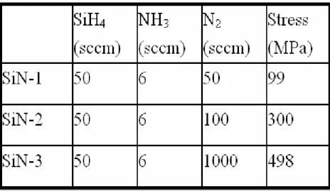
Table 3.1 Gas flow rate and mechanical stress for different nitride films ... 44
Fig.3.1 ID-VD Characteristics of different splits of NMOSFETs. Channel
length/width = 0.5μm /10μm. ... 45 Fig.3.2 Subthreshold characteristics and transconductance of different splits of
NMOSFETs. Channel length/width = 0.5μm /10μm
.
... 46 Fig.3.3 Subthreshold swing of different splits of NMOSFETs. Channellength/width = 0.5μm /10μm ... 47 Fig.3.4 Charge pumping current for three splits of fresh devices with
channellength/width = 0.5μm/10μm. Measurement was performed under fixed amplitude of 1.5 V and frequency of 1 MHz. ... 48
Fig.3.5 Increase in transconductance versus channel length. The
transconductance was measured at VG – Vth = -2 V and VDS = -2 V. ... 49
Fig.3.6 Capacitance-Voltage (C-V) characteristics of different splits of
NMOSFETs. Channel length/width = 50μm /50μm... 50 Fig.3.7 Dielectric constant characteristics of different splits of NMOSFETs. ... 51
Fig.3.8 Threshold voltage roll-off as a function of channel length for different
splits of samples... 52
Fig.3.9 Drain induced barrier lowing (DIBL) for different splits of NMOSFETs
as a function of channel length. DIBL was evaluated by measuring the
drain current change as VDS was increased at some fixed gate voltage
below threshold voltage. ... 53
Fig.3.10 Subthreshold characteristics and transconductance of devices before and
after 5000sec hot-electron stressing. Channel length/width = 0.5μm/10μm. (a) Control sample. (b) SiN-1 Capped sample. (c) SiN-2 Capped sample
(d).SiN-3 Capped sample... 54
Fig.3.11 Threshold voltage degradation of hot-electron stressing performed at VDS
= 4.6 V and VGS at maximum substrate current on all splits of devices
with channel length/width = 0.5μm/10μm.. ... 56 Fig.3.12 Interface trap density degradation of hot-electron stressing performed at
VDS = 4.6 V and VGS at maximum substrate current on all splits of devices
with channel length/width = 0.5μm/10μm. ... 57 Fig.3.13 Charge pumping current after 5000 second hot carrier stress
(VG@Isubmax and VDS = 4.6 V) for three splits of devices with channel
length/width = 0.5μm/10μm.. ... 58 Fig.3.14 Increase in charge pumping current after 5000 second hot carrier stress
(VG@Isubmax and VDS = 4.6 V) for three splits of devices with channel
length/width = 0.5μm/10μm. ... 59 Fig.3.15 Non-uniform distribution of local threshold voltage and flat-band voltage
across the device caused by the variation of lateral doping concentration..
... 60
Fig.3.16 Derivation of the relationship between local threshold voltage and lateral
distance x from the single junction charge pumping data of the control
device ... 61
Fig.3.17 Extracted lateral profile of local threshold voltage near the graded drain
junction in the control sample... 62
Fig.3.18 Charge pumping current before and after 10 second hot-electron
stressing (VG@Isubmax and VDS = 4.6 V). Channel length/width =
0.5μm/10μm. ... 63 Fig.3.19 Lateral profile of interface state generation under three different SiN
Chapter 1
Introduction
1-1 General Background and Motivation
1-1.1 Strained Channel Technology
The “Moore’s Law” was proposed in 1964 by Gordon Moore who was a
co-founder of Intel. The law states that the number of transistors integrated in a chip
will be doubled every two years. Although the period for one-fold increase in
transistor number is not precisely two years, for the past four decades the
power-dependence on time implicated by the law has been successfully applied to the
evolution trends of semiconductor industry. It can be said that the Moore’s Law has
been playing the role of driver to propel and advance the performance of the
integrated circuit (IC) performance. Furthermore, the Law may continue in the next
two decades as indicated by Morris Chang, the president of Taiwan Semiconductor
Manufacturing Company (TSMC).
The continuous shrinkage of device dimensions is the name of the game adopted
by the main-stream companies in the industry to follow and push the “Moore’s Law”.
The geometric scaling of Complementary Metal-Oxide- Semiconductor(CMOS) not
only increases the circuit integration density, but also enhances the transistor
performance. To address the short-channel effects, the device shrinkage has to be
scaling, thinner gate oxide and shallower junction depth are also essential to the
development of a new generation of technology.
As evolving into the nano-scale era, severe short channel effects pose a big
barrier ahead. Lowering in power supply voltage and ultra-shallow doping profile for
source and drain junctions could help, but these measures are often accompanied with
a penalty of drive current degradation. In addition, the increase in substrate doping
concentration in order to reduce short channel effects causes mobility degradation.
Recently strain channel engineering has demonstrated its capability to address these
issues, and thus becomes more and more popular for practical manufacturing [1-4]. To
this date at least two major strain channel technologies can be categorized. One is
accomplished by applying a high bi-axial tensile strain to the channel region with a
SiGe virtual substrate [1]. Another approach is to apply certain unique techniques to
induce uni-axial strain in the channel [2-5]. The latter approach is more attractive
because it can be easily implemented in modern Si CMOS processes. Uni-axial stress
usually exhibits better performance enhancement when channel length becomes
shorter [10-12]
Bi-axial tensile strain improves both NMOSFET and PMOSFET drive current by
altering the band structure of the channel and can therefore enhance performance even
Si channel layer on a relaxed SiGe substrate has been demonstrated. Drive current of
both NMOSFET and PMOSFET is enhanced by biaxial tensile stress when Ge is
incorporated by more than 20% in the relaxed SiGe layer. However, the yield issue
associated with high threading dislocation density (typically > 104 cm-2) of the virtual
SiGe substrates represents a major obstacle for practical applications. In addition,
others concerns, such as high Ge content and up-diffusion, fast diffusion of n-type
dopants, and high wafer cost, further blight the situation.
In order to find out a solution to eliminate the problems of the biaxial strain
channel techniques, a number of uniaxial strain channel techniques have been
proposed. In this aspect, channel strain can be engineered and optimized by modifying
the device processing and/or structure, including those steps involving
contact-etch-stop-layer (CESL)[13], shallow trench isolation (STI)[14], source/drain
material[15], silicicidation [16], packing process[17], and so on. Furthermore, the
behaviors of carrier mobility under uniaxial strain depend on the strength of the strain
and orientation. Electron and hole mobilities respond to the complex
three-dimensional mechanical stress in different and opposite ways. The channel
tensile and compressive stress can be applied separately to NMOS and PMOS devices
to enhance performance, respectively. It has been shown that the mechanical stress
affect the drive current. Depending on the deposition conditions, the SiN capping
layer can generate either tensile or compressive stress [18]. It thus can be applied to
the NMOS devices that benefit from tensile stress, as well as PMOS devices that
benefit from compressive stress. (Fig. 1.1)
The carrier distribution in energy valley, scattering rate, and effective mass are
the most significantly impact factors for mobility enhancement in strained-Si devices
( *
m qτ
μ = , where1/τ is the scattering rate and m* is the conductivity effective mass).
Strain enhances the mobility by reducing the effective mass and/or the scattering rate.
Both are important for mobility enhancement in electrons [19]. However, only
effective mass change due to band warping and repopulation [20] plays a significant
role in holes. For electron transports in bulk Si, the conduction band is composed of
six degenerate valleys (Δ6) of the same energy, as illustrated in Figure 1.2 [21]. Strain
removes the degeneracy between the four in-plane valleys (Δ4) and the two
out-of-plane valleys (Δ2) by splitting them in energy. (Fig. 1.3) The energy difference
(ΔE) between Δ2 and Δ4 sub-bands determines the total population in each sub-band.
The enhancement caused by the splitting of conduction band can suppress inter-valley
phonon scattering [22]. The lower energy of the Δ2 valleys indicates that they are
preferentially occupied by electrons. The electron mobility is improved partly by
mass of the Δ2 valleys, which results in more electrons with an in-plane transverse
effective mass and out-of-plane longitudinal mass.
For holes, the valance-band structure of Si is more complex than the
conduction-band structure. The complex band structure as well as valence-band
warping under strain results in a much larger mobility enhancement of holes than
electrons. This is why strained-channel PMOSFETs is a key focus in advanced logic
technologies. Holes occupy the top two (the heavy- and light- hole) bands for
unstrained Si. With the application of strain, the hole effective mass becomes highly
anisotropic due to band warping, and the energy levels become mixtures of the pure
heavy, light, and split-off bands. Thus, the light and heavy hole bands lose their
meaning, and holes increasingly occupy the top band at higher strain due to the
energy splitting. To quantify the mobility enhancement of holes, changes of scattering
and effective mass depend on the altered valance band caused by the strain. From full
band Monte Carlo simulation [23], PMOSFETs with uni-axial compressive stress may
have lighter in-plane effective mass and thus show improved hole mobility. But, for
biaxial tensile stress, the effective mass is heavier than that in the unstrained case.
Thus the hole mobility enhancement is only possible through the reduction of
inter-valley scattering [24]. This effect becomes significant only when the strain level
the density- of-states of the light- and heavy-hole bands is negligible for uni-axial
strain in Si, even at several hundreds of mega-pascal.
The mobility enhancement of uni-axial strain at high vertical electric field is
higher than that of the bi-axial case. This represents another advantage of uni-axial
strain over the bi-axial strain. Hole mobility at high vertical field would have different
behaviors between uni-axial compressive and biaxial tensile stress. The splitting of
light- to heavy-hole band caused by uni-axial and biaxial stresses has no significant
difference without considering surface quantization confinement. However, the
splitting of light- and heavy-hole bands caused by bi-axial tensile stress would be
annulled at high electric field due to surface confinement [11]. In contrast, hole
mobility enhancement under uni-axial compressive strain is not annulled by surface
confinement, which represents a major advantage for MOSFETs operating at high
electric fields. The splitting magnitude of the surface confinement depends on the
relative magnitude of the stress altered light and heavy hole out-of-plane effective
masses. A recent report [11] showed the interesting result that the out-of-plane
effective mass of light hole is heavier than heavy hole for uni-axial stress and causes
the light to heavy hole band splitting to increase. On the contrary, for bi-axial stress
the previously-reported out-of-plane effective mass of light hole is lighter than heavy
degrades hole mobility enhancement at high vertical electric fields.
In strained-Si NMOSFETs, the strain will induce valence band offset. The
negative valence band offset makes the Fermi level closer to the conduction band,
thus, the band offset lowers the threshold energy and makes the channel depletion
shallower. The fact that the threshold voltage shift caused by bi-axial tensile stress is
larger than the case with uni-axial tensile strain has been reported for NMOSFETs
[25]. This is because the bi-axial tensile stress induces more band gap narrowing than
uni-axial tensile strain case. Similarly for PMOSFETs, larger shift of light-hole band
edge under bi-axial tensile strain leads to larger shift in Vth than the case with
uni-axial compressive strain [26].
1-1.2 Hot Carrier Effects
The knowledge of mobility enhancement in strain-Si is well known. It is found
that it can effectively boost the driving current, but the issue of reliability remains a
concern. In this aspect, device degradation induced by hot electrons represents one of
the most critical reliability issues in deep sub-micron NMOSFETs [5-6], and have
been widely investigated [7-8] previously. The degradations in terms of threshold
voltage shift (ΔVth), drain current degradation (ΔIDS), and transconductance
degradation (ΔGm), are observed in the accelerated stress test.
unchanged, the lateral electric field in the channel increases significantly. The
inversion layer charges will be accelerated more significantly, resulting in the
generation of hot carriers, which may lead to undesired defect formation when they
release energy at the channel/oxide interface or in the oxide. The mechanisms
mentioned above are called hot-carrier degradation. It causes a time-dependent
degradation of various MOSFET parameters, for example, threshold voltage, linear
transconductance, subthreshold slope, and saturation slope, and saturation current.
The locations of damage region due to hot-carrier stressing were found to be
adjacent to the drain of the device. The lifetime of the device is impacted by the
spatial non-uniformity of this damage. The damaged locations and extent depend on a
number of factors like device geometry, the duration and conditions of stress, oxide
thickness, and drain extension structure. It was reported that the length of damaged
region is more or less independent of channel length [27], its influence on device
performance becomes more significant as the device is shrunk. This causes a dramatic
increase in the percentage of drive current degradation as channel length becomes
shorter under the same stress conditions.
1-2 Motivation
As mentioned above, the SiN layer can be used to induce channel strain for
hydrogen spicies will be incroporated into the channel which may significantly affect
device reliability. In particular for NMOSFETs, despite the dramatic improvement in
device performance with tensile SiN capping, their hot-carrier relability is, however,
compromised. In one of our group’s previous studies, we characterized the NMOS
devices capped with a highly tensile SiN stressor layer. Although the stressor indeed
showed improvement in carrier mobility and device drive current, we found that the
extra hydrogen species incorporated during SiN deposition has undesirable influence
on hot carrier reliability [9]. To reduce the impact of hydrogen without compromising
the induced strain remains an important task. This motivates us to carry out this study
intended to develop optimized SiN deposition conditions using plasma enhanced
chemical vapor deposition (PECVD) system. The desirable SiN capping layers should
have the ability to induce suitable stress in the channel but have reduced hydrogen
content to avoid significantly degrading the hot-carrier reliability.
1-3 Organization of This Thesis
In addition to this brief introductory chapter, this thesis contains the following
three chapters and their contents are described below:
In Chapter 2, we briefly describe the process flow for fabricating the NMOS
devices with the SiN capping layer. We also present the characterization methods,
In Chapter 3, we show and discuss the improvement on device performance with
SiN capping layer by PECVD. The results on evaluating the hot carrier characteristics
of the locally strained devices are presented. Effects of strain on the hot carrier effects
are also discussed.
Finally, important conclusions generated from our experimental results are
summarized. Certain recommendations and suggestions for future work are also given
Chapter 2
Device Fabrication and Measurement
Setup
2-1 Device Fabrication and Process Flow
NMOSFETs used in this study were fabricated on 6-inch p-type (100) Si wafers
with resistivity of 15~25Ω-cm and the wafer thickness is 655~695 μm. The p-type
well was formed first by BF2+ implantation at 100 keV and 1×10-13 cm-2. Standard
local oxidation of silicon (LOCOS) process with channel stop implant (by BF2+
implantation at 120 keV and 4×10-13 cm-2) was used for device isolation. Threshold voltage adjustment and anti-punch through implantation steps were done by
implanting 40 keV BF2+ and 35 KeV B+, respectively. After the growth of 3 nm-thick
thermal gate oxide, a 150nm undoped poly-Si layer was deposited by low-pressure
chemical vapor deposition (LPCVD), followed by gate etch process to pattern the film.
The source/drain (S/D) extension regions were then formed by As+ implantation at 10
keV and 5×10-14 cm-2. After a TEOS spacer formation, S/D regions were formed by P+ implantation at 15 keV and 5×10-15 cm-2. Then the substrate electrode patterning was performed through lithography and etching processes, and the substrate junction was
formed by BF2+ implantation at 40 keV and 5×10-15 cm-2. Rapid thermal anneal(RTA)
the gate, S/D, and substrate regions.
Afterwards, most samples were capped with a SiN capping layer (passivation
layer,) under different flow rate ratio of N2/SiH4 (1, 2 and 20), with a thickness of
300nm, by using a plasma-enhanced chemical vapor deposition (PECVD) system.
While some wafers were deliberately skipped of the SiN capping layer to serve as the
controls. The SiN deposition was performed at 300 ℃ with SiH4, N2, and NH3 as the
reaction precursors. Then a 300nm TEOS was deposited for passivation by the same
PECVD system.
The SiN layers used in the above fabrications exert tensile stress on the Si wafer
it capped. To confirm the effects of different stress types on electrical characteristics
of the fabricated devices, we also fabricate some devices capped with a compressive
300nm-thick SiN layer. The layer was deposited using another PECVD system.
After contact hole etching, normal metallization scheme was carried out. The
final step was a forming gas anneal performed at 400°C for 30 min to mend dangling
bonds and reduce interface state density in gate oxide/Si interface. Cross sectional
view of the fabricated device is shown in Fig. 2.1. The three different conditions of
the capping layers are listed in Table 2.1.
2-2 Measurement Setup
Current-voltage (I-V) and capacitance-voltage (C-V) characteristics were
evaluated by an HP4156A precision semiconductor parameter analyzer and an
HP4284 LCR meter, respectively. Temperature-regulated hot chucks were used to
control and fix the temperature at 25°C.
Charge pumping measurement is widely used to characterize interface state
densities in MOSFET devices [28]. This type of measurement is very effective
because it allows the exclusion of gate leakage contribution to the calculated interface
state densities presented in thin gate oxides and at lower frequencies [29-30].
Therefore, to accurately analyze interface state densities or bulk traps in the
dielectrics from charge pumping measurement results, we need to pay close attention
to the leakage current issue. The basic charge pumping measurement includes the
measurement of the substrate current while a series of voltage pulses with fixed
amplitude, rise time, fall time, frequency, and duty cycle is being applied to the gate
of the transistor (Figure 2.2), with source and drain connected to a small reverse bias,
and substrate tied to the ground. This seup allows us to apply three conventional types
of voltage pulse train to the gate electrode, as depicted in Figure 2-3, i.e., (a) fixed
amplitude sweep, (b) fixed base sweep, and (c) fixed peak sweep.
In this thesis, “fixed amplitude sweep” was used to calculate interface trap
interface trap, respectively. Square-wave waveforms (f = 1MHz) were applied to the
gate, and the base voltage was varied to let surface condition from inversion to
accumulation, while keeping the pulse amplitude at 1.5V. A MOSFET with a gate area
of AG gives the charge pumping current as [31]:
cp G it
I =qA fN (2-1)
, and interface trap density (Nit) could be calculated by using this formula.
2-2.2 Hot Carrier Reliability Measurement Setup
In our reliability measurement, the device was stressed with the drain voltage
biased at a highly positive voltage, and the gate biased at the voltage where maximum
Isub occurred to accelerate the degradation. So we must first measure the Isub-VG
curve with the drain terminal biased at a fixed voltage to find VG@Isubmax, before we
performed the hot-carrier stressing. To monitor the degradation caused by the hot
electrons, the ID-VG characteristics at VDS = 0.05 V (linear region) and charge
pumping current were measured before and after the stress. The degradations in terms
of threshold voltage shift (ΔVth), interface trap density degradation (ΔNit), and
transconductance degradation (ΔGm), were observed in the accelerated stress test.
2-2.3 Extraction Procedure of Lateral Distribution of Nit
The lateral distribution of interface state post hot carrier stress of all splits was
also discussed in this work. This method was built on [32] and the measurement setup
(1) Measure the Icp-Vh curve on a virgin MOSFET from the drain junction (with the
source junction floating), and from it establish the Vh versus Vth(x) relationship[32]
near the junction of interest.
(2) Record the Icp-Vh curve after hot-carrier injection.
(3) The hot-carrier-induced interface state distribution, Nit(x), is obtained from the
Chapter 3
Results and Discussion
3-1
Electrical Characteristics of Locally Strained NMOSFETs
3-1.1 Basic Electrical Characteristics
The stress measurements were performed on Si wafers capped with a blanket
SiN layer with different flow rate ratio of N2/SiH4. The results are showed in Table
3.1 It can be seen that the tensile stress becomes larger when N2/SiH4 flow rate ratio is
larger. This is reasonable as the thermal expansion coefficient of a deposited film
depends on the film’s composition which can be adjusted by varying the flow rate of
precursors.
Figure 3.1 shows ID-VD Characteristics of NMOSFETs for all splits of samples.
It can be seen that Tensile-SiN-capped splits depict an obvious drain current
enhancement with respective to the control devices. Further, the enhancement
increases as flow rate ratio (N2/SiH4) increases. In contrast, current degradation is
observed for the Compressive-SiN-capped samples. Obviously the current
enhancement and degradation is straightly due to the strain type and magnitude of the
strain introduced by the SiN capping layer. The Id-Vg characteristics of the same
devices are shown in Fig 3.2. We can see that the impact of SiN-capping layer
mentioned above also reflects on the result of transconductance (Gm). Fig 3.3 shows
lower than that of TEOS control. This is ascribed to the hydrogen species contained in
the SiN that tends to passivate the interface states, resulting in better subthreshold
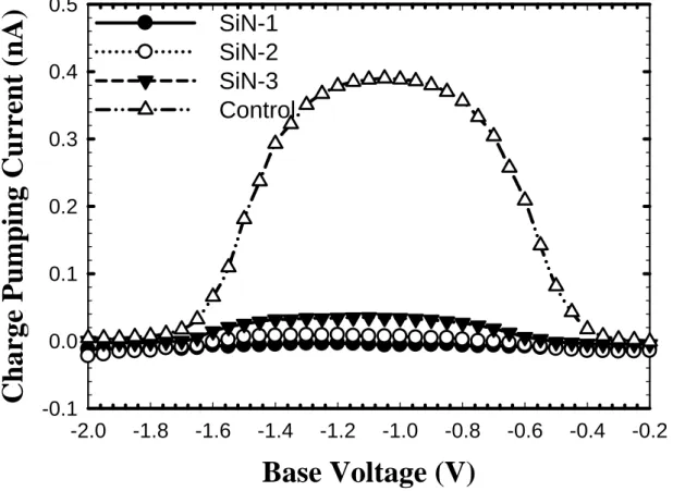
swing among the splits. This is evidenced from the results of charge pumping current
(Icp), as shown in Fig. 3.4. Obviously, all SiN capping splits have lower Icp than
TEOS controls.
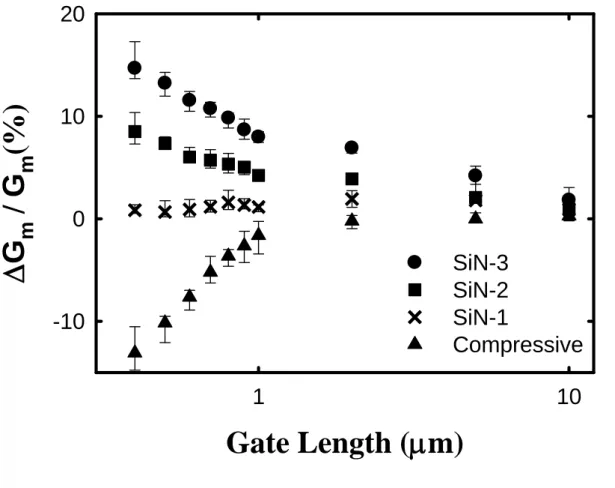
Fig 3.5 shows the percentage change in transconductance (Gm) of the Tensile-SiN-capped and Compressive-SiN-capped samples with respect to the
controls, as a function of channel length. We can see that the drive current
enhancement reaches about 0.8%, 8.8%, and 15.4% at a channel length of 0.4 μm for
Tensile-SiN capped devices with N2/SiH4 flow rate ratio of 1, 2, and 20, respectively,
while the device capped with compressive SiN shows about -12.6% degradation. It
can also be seen that when the channel length decreases, the strain effect enhances. In
other words, the strain is distributed locally near the source and drain, and the overall
impact becomes more significant as channel length is shorter. The capacitance-voltage
characteristics of the samples are shown in Fig 3.6. It can be seen that the oxide
thickness difference among all splits is negligible, indicating that the
above-mentioned results are not caused by the oxide thickness difference. The poly
depletion effect is not observed in the SiN-Capped devices. From our group’s
deposited to serve as the tensile strain booster. The LPCVD process was performed at
a medium temperature of 780˚C which had a much lower solid solubility than high
temperature [33](e.g., 950 ℃, the RTA temperature used in the fabrication to active the
dopants in the poly). Since the PECVD process was performed at 300˚C which was so
low that the associated thermal budget would not affect the activated carrier
concentration, therefore the poly depletion effect did not get worse.
It is well known that the use of interlayer dielectric will increase RC time delay.
The dielectric constant of the deposited SiN film should thus be considered. Fig 3.7
shows the dielectric constant of different SiN film, it is clearly seen that there is no
distinct difference among all splits of samples, thus these deposited films would not
worsen the RC-delay issue. .
3-1.2 Short Channel Effects
Threshold voltage (Vth) roll-off characteristics of the devices are shown in Fig.
3.8. The results are obtained at VDS = 0.05 V. It is shown that all samples depict a
reverse-short-channel-effect (RSCE). This can probably be explained by boron
segregation at the implant-damaged regions located near the edge of the channel.
Additional thermal budget may alleviate the reverse-short-channel-effect. It might be
related to the redistribution of dopants that effectively reduced the boron segregation
operated at 300 ℃, a temperature too low to redistribute the dopants in the channel, it
thus has negligible influence on this phenomenon.
Drain induced barrier lowing (DIBL) is another guide for evaluating the short
channel effects. We use the interpolation method to calculate DIBL effect for all splits
of devices. The results are shown in Fig. 3.9, basically no distinct difference among
different splits is observed. It points out that SiN capping layer does not complicate
the DIBL effect of the samples.
3-2
Hot Carrier Degradation of Locally Strained
NMOSFETs
From the discussion mentioned in Chapter 1, it is expected that devices with SiN
capping would encounter serious hot carrier degradation. Typical results of
hot-electron stressing for the control and three other splits are shown in Fig 3.10.
Channel length and width of the test devices are 0.5 μm and 10 μm, respectively. The
devices were stressed at VDS = 4.6 V and VGS at maximum substrate current. The
ID-VG characteristics at VDS = 0.05 V were measured before and after the stress to
check the degradation caused by the hot electrons. As shown in Fig 3.10, the
degradation is the worst in the SiN-1 sample among all samples. Fig. 3.11 and Fig.
of stress time for all splits of samples, respectively, of hot-electron stressing at VDS =
4.6 V and VGS at maximum substrate current performed on all splits of devices with
channel length/width = 0.5μm/10μm. As can be seen in the figures, the effect of flow
rate of precursors in SiN deposition is significant. We can see that the device lot with
ratio of N2/SiH4=1 depicts the worst degradation in terms of the largest ΔVth. By
contrast, the lot with flow rate ratio N2/SiH4=20 apparently shows much improvement
in this aspect, although it also results in the largest mobility and on-current
enhancement. Increase in interface state generation (ΔNit) shows the same trend. This
finding is interesting and important, and is ascribed to the hydrogen content and the
dynamic transport of these hydrogen species by the thermal cycles during processing.
It is well known that the breaking of Si-H bonds at the interface is one of the major
reasons responsible for the hot-carrier degradation. The abundant hydrogen species
contained in the SiN definitely aggravate the reliability. Hydrogen atoms tend to bond
with nitrogen for nitrogen-rich film with increasing N2 flow rate, N-H bonds are
thermally more stable than Si-H bonds [35]. This may result in less diffusion of
hydrogen species from the SiN to the oxide/channel interface. In addition, less Si-H
bonds is expected for flow rate ratio of N2/SiH4=20, since N2 instead of NH3 serves as
the major nitrogen source. More evidences can be found in Fig. 3.13 and Fig 3.14. Fig.
(VG@Isubmax and VDS = 4.6 V) for the three splits of devices, and Fig. 3.13 shows the
increase in charge pumping current after the stressing. As mentioned above, the
hydrogen species contained in the SiN tends to passivate the interface states. More
H-terminated bonds at the interface are expected for the SiN-1 split, and these bonds
would dissociate and result in largest increases in charge pumping current shown in
the figures. In contrast, it is seen that the SiN-1 and SiN-3 samples exhibit less
generated interface states among the three Tensile-SiN-capped devices, implying
H-terminated bonds are dramatically reduced.
3-3 Analysis of the Distribution of Interface Trap Density
The measurement presented in Section 2-2.3 was used to extract lateral
distribution of interface trap state. It should be noted that the local Vth and Vfb, across
the MOSFET, are not uniform due to the lateral doping variation with a schematic like
that shown in Fig. 3.15. In order to detect the interface states, the pulse train during
the measurement must undergo alternate accumulation and inversion cycles. There
should be no Icp as the voltage level of the high-voltage (Vh) is lower than the
minimum Vth under the gate. When Vh starts to exceed Vth at certain channel locations
under the gate, Icp begins to grow. From the profile illustrated in Fig. 3.15, before Vh
reaches the maximum local Vth in the channel, interface states that contribute to Icp
cannot yet flow to the drain side from the source.
We choose the control sample as an example. If we assume that interface state
density is spatially uniform along the channel, which can be written as
,max
cp it
I =q f N W L (3-1)
where f is the gate pulse frequency, W the channel width, and L the channel length.
Because Vth is not uniform, when Vh reaches the maximum local Vth in the channel,
only interface states residing near the drain side (like the shadow region in Fig. 3.15)
will contribute to Icp. In Fig. 3.16, the corresponding Icp (Vh) comes from the
interface states distributed between the gate edge and the position where its local Vth
is equal to Vh, i.e.,
( )
cp h it
I V =q f N W x (3-2)
where x represents the distance from the gate edge to the position where Vth (x) = Vh.
Comparing (3-1) and (3-2), we can derive
( )
max , cp h cp I V LI x= (3-3)Fig. 3.17 shows the local Vth versus distance x of the control sample. The local Vth
decreases sharply as x is smaller than 0.07 μm. We can therefore presume that the
drain junction is near x = 0.07 μm.
After 10 second hot carrier stress (VG@Isubmax and VDS = 4.5 V), the
at a certain Vh is proportional to the number of generated interface traps from the gate
edge to the point x, and can be expressed as
( )
0 x cp it I q f W N x dx Δ =∫
(3-4)Therefore, Nit(x) generated by the hot carrier stress can be extracted using the following formula:
( )
1 1 cp cp h it h d I d I dV N x dx q f W dV dx q f W Δ Δ = = (3-5) The relationship of dVhdx versus x can be derived from Vh versus x, so the lateral
distribution, Nit (x), can be obtained from the measurement scheme mentioned above.
By utilizing the same procedure, the derived lateral profiles of the interface state
distribution with all splits, extracted by Eq. (3-5), are shown in Fig. 3.19. From Fig.
3.19, we can realize and compare the damage region and amount of interface states
generated by hot carrier stressing. We can see that the damage region is confined
within the drain edge in all splits, which is reasonable since the degradation is
confined t the drain edge under the HC stressing. It is obviously seen that the SiN-1
samples show larger degradation than the other splits. These results were consistent
with the results and discussion mentioned in Section 3-2. In other words, the more
hydrogen species exist at the source/drain edge, the larger interface states are
Chapter 4
Summary and Conclusion
4-1 Conclusion
In this thesis, the effects of PECVD SiN process and the channel strain induced
by the SiN-capping layer on the device characteristics and hot-electron degradation
were investigated. Several important phenomena were observed and summarized as
follows.
Firstly, the channel strain induced by the tensile SiN capping layer over the gate
greatly boosts the drive current of short-channel NMOS devices. For example, as high
as 15.4 % enhancement is achieved for the SiN-capped NMOS devices with a flow
rate ratio of N2/SiH4=20 at a channel length of 0.4 μm. This is ascribed to the large
difference in the expansion coefficient between SiN film and Si-substrate. Since
n-channel devices with a compressive SiN capping layer show lower Gm than the
control samples, it can be confirmed that either current enhancement or current
degradation can be observed by varying the strain polarity. In addition, we also find
that without the associated thermal budget, the deposition of the PECVD SiN capping
layer can not alleviate the reverse short-channel effect of the devices, and the
poly-depletion effect will not be enhanced. Finally, we find that the dielectric constant
other two splits with different flow rate ratio.
Secondly, hot-electron degradation is negatively affected when the SiN layer is
deposited over the gate. However, we find that the negative impact in reliability can
be alleviated by properly tuning the flow rate of SiH4 and N2. The hydrogen atoms
tend to bond with nitrogen for nitrogen-rich film with increasing N2 flow rate,
resulting in less diffusion of hydrogen species from the SiN to the oxide/channel
interface.
In conclusion, we find that for the SiN-capped NMOS devices, the electrical
performance and reliability both improve with increasing N2 flow rate. In other words,
SiN-capped devices with optimized SiN deposition condition can maintain enhanced
mobility while showing alleviated hot-carrier degradation. Optimization of both SiN
deposition process and the film properties is therefore essential for the
References:
[1] J. L. Hoyt, H. M. Nayfeh, S. Eguchi, I. Aberg, G. Xia, T. Drake, E. A. Fitzgerald,
and D. A. Antoniadis, “Strained silicon MOSFET technology”, IEDM Tech. Dig.,
pp.23-26, December 2002.
[2] T. Ghani, M. Armstrong, C. Auth, M. Bost, P. Charvat, G. Glass, T. Hoffmann, K.
Johnson, C. Kenyon, J. Klaus, B. McIntyre, K. Mistry, A. Murthy, J. Sandford,
M. Silberstein, S. Sivakumar, P. Smith, K. Zawadzki, S. Thompson, and M.
Bohr, “A 90nm high volume manufacturing logic technology featuring novel
45nm gate length strained silicon CMOS transistors”, IEDM Tech. Dig.,
pp.978-980, December 2003.
[3] S.Pidin, T. Mori, K. Inoue, S. Fukuta, N.Itoh, E. Mouth, K. Ohkoshi, R.
Nakamura, K. Kobayashi, K. Kawamura, T. Saiki, S. Fukuyama, S. Satoh, M.
Kase, and K. Hashimoto, “A novel strain enhanced CMOS architecture using
selectively deposited hogh tensile and high compressive silicon nitride films”, in
IEDM .Tech.”Dig., pp. 213-216, 2004.
[4] C. Y. Lu, H. C. Lin, Y. F. Chang, and T. Y. Huang “Device characteristics and
aggravated negative bias temperature instability in PMOSFETs with uniaxial
compressive strain”, int. Conference on Solid State Devices and Materials, pp.
[5] E. Li, E. Rosenbaum, J. Tao, and P. Fang, “Projecting lifetime of deep submicron
MOSFETs”, IEEE Trans. on Electron Devices, vol. 48, pp. 671-678, Apr. 2001
[6] H. S. Momose, S. Nakamura, T. Ohguro, T. Yoshitomi, E. Morifuji, T. Morimoto,
Y. Katsumata, and H. Iwai, “A study of hot-carrier degradation in n- and
p-MOSFETs with ultra-thin gate oxides in the direct-tunneling regime”, in
IEDM Tech. Dig., 1997, pp. 453-456.
[7] A. Schwerin, W. Hansch, and W. Weber, “The relationship between oxide charge
and device degradation: A comparative study of n- and p- channel MOSFET's”,
IEEE Trans. on Electron Devices, vol. ED-34, pp. 2493-2500. Dec. 1987.
[8] P. Heremans, R. Bellens, G. Groeseneken, and H. Maes, “Consistent model for
the hot-carrier degradation in n-channel and p-channel MOSFETs”, IEEE Trans.
on Electron Devices, vol. 35, pp. 2194-2209. Dec. 1988.
[9] C. Y. Lu, “A Study of Device Current Enhancement Methods and Related
Reliability Issues for MOSFETs”, A Dissertation in Department of Electronics
Engineering & Instisute of Electronics in NCTU, pp. 122-148. July 2006
[10] S. Takagi, T. Mizuno, T.Tezuka, N. Sugiyama, T. Numata, K.Usuda, Y. M
oriyama, S. Nakaharai, J. Koga, A. Tanabe, N. Hirashita, and T
Maeda , ”Channel structure design, fabrication and carrier transport properties
Tech.Dig.,pp.57-60, December 2003.
[11] S. E. Thompson, M. Armstrong, C. Auth, S. Cea, R, Chau, G. Glass, T, Hoffman,
J. Kaus, Z. Ma, B. Mcintyre, A. Murthy, B, Obradovic, L. Shifren, S.
Sivakumar,S. Tyagi, T. Ghani, K. Mistry, M. Bhor, and Y. El-Mansy,”A logic
nanotechnology featuring strained-silicon”,IEEE Electron Device Lett, vol.
25,pp.191-193. April 2004.
[12] W. Zhao, J.He, R. E. Belford, L. Wernersson, and A. Seabaugh, “Partially
depleted SOI MOSFETs under uniaxial tensile strain”. IEEE Trans. Electron
Device, vol. 51,pp.317-323,March 2004.
[13] A. Shimizu, K. Hachimine, N. Ohki, H. Ohta, M. Koguchi, Y. Nonaka, H. Sato,
and F. Ootsuka, “Local mechanical-stress control (LMC): A new technique for
CMOS-performance enhancement”, IEDM Tech. Dig., pp. 433 - 436, December
2001.
[14] G. Scott, J. Lutze, M. Rubin, F. Nouri, and M. Manley, “NMOS drive current
reduction caused by transistor layout and trench isolation induced stress”, IEDM
Tech. Dig., pp.827-830, December 1999.
[15] T. Matsumoto, S. Maeda, H. Dang, T. Uchida, K. Ota, Y. Hirano, H. Sayama, T.
Iwamatsu, T. Ipposhi, H. Oda, S. Maegawa, Y. Inoue, and T. Nishimura, “Novel
<100>-channel for embedded RF/analog applications,” IEDM Tech. Dig.,
pp.663-666, December 2002.
[16] A. Steegen, M. Stucchi, A. Lauwers, and K. Maex, “Silicide induced pattern
density and orientation dependent transconductance in MOS transistors”, IEDM
Tech. Dig., pp.497-500, December 1999.
[17] S. Maikap, M. H. Liao, F. Yuan, M. H. Lee, C. Huang, S. T. Chang, and C. W.
Liu, ”Package-strain-enhanced device and circuit performance”, IEDM Tech.
Dig., pp.233-236, December 2004.
[18] S. Ito, H. Namba, K. Yamaguchi, T. Hirata, K. Ando, S. Koyama, S. Kuroki, N.
Ikezawa, T. Suzuki, T. Saitoh, and T. Horiuchi, “Mechanical stress effect of
etch-stop nitride and its impact on deep submicron transistor design”, IEDM
Tech. Dig., pp.247-250, December 2000.
[19] C. Zhi-Yuan, M. T. Currie, C. W. Leitz, G. Taraschi, E. A. Fitzgerald, J. L. Hoyt,
and D. A. Antoniadis, “Electron mobility enhancement in strained-Si
n-MOSFET fabricated on SiGe-on-insulator (SGOI) substrates”,IEEE Electron
Device Lett.,vol.22,pp.321-323, July 2001
[20] S. E. Thompson, G. Sun, K. Wu, J. Kim, and T. Nishida, “Key differences for
process-induced uniaxial vs. substrate-induced biaxial stressed Si and Ge
[21] 林宏年, 呂嘉裕, 林鴻志, 黃調元, “局部與全面形變矽通道(strained Si
channel)” 互補式金氧半(CMOS) 之材料,製程與元件特性分析(I)”, 奈米通
訊第十二卷第一期
[22] B.M. Haugerud, L. A. Bosworth, and R. E. Belford, “Mechanicallt induced strain
enhancement of metal—oxide—semiconductor field effect transistors”,J.
APPL.phys.,Vol.94,pp.4102-4107, 2003
[23] M.D.Giles, M.Armstrong. C.Auth, S.M.Cea, T.Ghani, T.Hoffmann, R.Kotlyar,
P.Matagne, K.Mistry, R.Nagisetty, B.Obradovic, R.Shaheed, L.Shifren,
M.Stettler, S.Tyagi, X.Wang, C.Weber, K.Zawadzki, “Understanding stress
enhanced performance in Intel 90nm CMOS technology”,VLSI Symp. Tech.
Dig.,pp.118-119,2004”
[24] C. W. Leitz, M. T. Currie, M. L. Lee, Z.-Y. Cheng, D. A. Antoniadis and E. A.
Fitzgerald, “Hole mobility enhancements and alloy scattering-limited mobility
in tensile strained Si/SiGe surface channel metal–oxide–semiconductor
field-effect transistors”, J. Appl. phys., Vol.92, pp.3745-3751, 2002
[25] C. Ge, C. Lin, C. Ko, C. Huang, Y. Huang, B. Chan, B. Perng, C. Sheu, P. Tsai,
L. Yao, C. Wu, T. Lee, C. Chen, C. Wang, S. Lin, Y. Yeo, and C. Hu,
“Process-strained Si (PSS) CMOS technology featuring 3D strain engineering”,
[26] J. Welser, J. L. Hoyt, S. Takagi, and J. F. Gibbons,” Strain dependence of the
performance enhancement in strained-Si n-MOSFETs”, IEDM Tech. Dig.,
pp.373-376, December 1994.
[27] H. Hazama, M. Iwase, and S. Takagi, “Hot-carrier reliability in deep
sunmicrometer MOSFETs”, in IEDM Tech. Dig.,pp.569-572, 1990
[28] G. Groeseneken, H. E. Maes, N. Beltran, and R. F. Dekeersmaecker, “ A reliable
approach to charge-pumping measurements in MOS transistor,” IEEE
Transactions on Electron Devices, Vol. ED-31, pp42-53, 1984.
[29] S. S. Chung, S.-J. Chen, C.-K. Yang, S.-M. Cheng, S.-H. Lin, Y.-C. Sheng,
H.-S. Lin, K.-T. Hung, D.-Y. Wu, T.-R. Yew, S.-C. Chien, F.-T. Liou, and F,
Wen , “A novel and direct determination of the interface Traps in sub-100nm
CMOS devices with direct tunneling regime (12-16Å) gate oxide,” VLSI Tech.
Symposium, 2002.
[30] Pascal Masson, Jean-Luc Autran, and Jean Brini, “On the tunneling component
of charge pumping current in ultrathin gate oxide MOSFET’s,” IEEE Electron
Device Lett., pp. 92-94, 1999
[31] Dieter K. Schroder, “Semiconductor material and device characterization,”
Second Edition.
charge and interface traps in thin gate MOSFET’s”, IEEE Electron Devices,
vol.45, pp.512-520, Feb. 1998.
[33] S.N.Sze,Physics of semiconductor Devices, vol. 40, pp. 69, July 1985
[34] L. Chang, S. Tang, T.J. King, J. Bokor, and C. Hu,”Gate length scaling and
threshold voltage control of double-gate MOSFETs”,in IEDM Tech Dig., 2000,
pp. 719-722.
[35] M. Yamamura, T. Matsuki, “Improvement in NBTI by Catalytic-CVD Silicon
Fig. 1.2 Simple schematic of conduction and valence band bending with strain.[21]
Fig. 1.3 Schematic diagram of the energy sub-bands with unstrained and bi-axial strain in an MOS inversion layer.[26]
Gate
SiN Passivation
Layer
(Flow rate ratio= N2/ SiH4)
W/O (control)
Flow rate ratio:1
SIN 3000Å
Flow rate ratio:2
SIN 3000Å
Flow rate ratio:20
SIN 3000Å
Oxide
30Å
Undoped
Poly-Si
1500Å
Compressive
SIN 3000Å
Fig 2.1 Schematic cross section of the local strained channel NMOSFET
P-substrate
P-well
FOX
FOX
P
+P
+Poly
-Si
N
-N
-oxideN
+N
+SiN
SiN
Source
Drain
Gate
Fig . 2.2 Setup structure for charge pumping. Switch HP 4156 GPIB p-substrate n+ Source n+ Drain n+ Gate e -h+ HP 81110A Pulse Generator
Fig.2.3 Schematic illustrations for the charge pumping measurement with (a) fixed amplitude, (b) fixed base sweep, and (c) fixed peak sweep. The arrows indicated the sweep directions.
V
thV
fb(a)
Vh VlV
thV
fb Vh Vl(b)
Vh VlV
thV
fb(c)
Fig. 2.4 The measurement setup of single junction charge pumping measurement
Icp
Floating
n
+Drain
n
+Source
n
+Gate
Fixed base mode
V
base=-0.1V,
V
h=-0.8V ~ -1V
V
baseV
hTable 3.1 Gas flow rate and mechanical stress for different nitride films deposited by PECVD.
Drain Voltage(V)
0.0
0.5
1.0
1.5
2.0
Drain Current(mA)
0
1
2
3
4
5
6
Control SiN-1 SiN-2 SiN-3 CompressiveFig.3.1 ID-VD Characteristics of different splits of NMOSFETs. Channel length/width
Gate Voltage (V) -1.0 -0.5 0.0 0.5 1.0 1.5 2.0 D ra in Current (A) 10-14 10-13 10-12 10-11 10-10 10-9 10-8 10-7 10-6 10-5 10-4 10-3 10-2 10-1 control SiN-1 SiN-2 SiN-3 Compressive
Gate Voltage (V)
-0.2 0.0 0.2 0.4 0.6 0.8 1.0 1.2 1.4Trans
conductance (
μS)
0 100 200 300 400 Control SiN-1 SiN-2 SiN-3 CompressiveFig.3.2 Subthreshold characteristics and transconductance of different splits of
con
trol
SiN
-1
SiN
-2
SiN-
3
com
pre
ssiv
e
Subthreshold Swing (mV/dec)
70
72
74
76
Fig. 3.3 Subthreshold swing of different splits of NMOSFETs. Channel length/width
Base Voltage (V)
-2.0 -1.8 -1.6 -1.4 -1.2 -1.0 -0.8 -0.6 -0.4 -0.2
Charge Pumping Current (nA)
-0.10.0 0.1 0.2 0.3 0.4 0.5
SiN-1
SiN-2
SiN-3
Control
Fig. 3.4 Charge pumping current for three splits of fresh devices with
channellength/width = 0.5μm/10μm. Measurement was performed under fixed amplitude of 1.5 V and frequency of 1 MHz.
Gate Length (
μm)
1
10
Δ
G
m
/
G
m
(%)
-10
0
10
20
SiN-3
SiN-2
SiN-1
Compressive
Fig. 3.5 Increase in transconductance versus channel length. The transconductance
Gate Voltage (V)
-2 -1 0 1 2Capacitance (
μF/cm
2
)
0.2 0.4 0.6 0.8 1.0 1.2 Control SiN-1 SiN-2 SiN-3 CompressiveFig. 3.6 Capacitance-Voltage (C-V) characteristics of different splits of NMOSFETs.
SiN-1
SiN-2
SiN-3
TEOS
K Constant
4.5 5.0 5.5 6.0 6.5
Gate Length (
μm)
1
10
Δ
Vth (mV)
0
10
20
30
40
50
60
Control
SiN-1
SiN-2
SiN-3
Compressive
Fig. 3.8 Threshold voltage roll-off as a function of channel length for different splits
Gate Length (
μm)
0.3
0.4
0.5
0.6
0.7
0.8
0.9
1.0
1.1
DIBL (mV/V)
4
6
8
10
12
Control SiN-1 SiN-2 SiN-3Fig. 3.9 Drain induced barrier lowing (DIBL) for different splits of NMOSFETs as a
function of channel length. DIBL was evaluated by measuring the drain current change as VDS was increased at some fixed gate voltage below
Gate Voltage (V)
0.0 0.2 0.4 0.6 0.8 1.0 1.2 1.4 1.6
Drain Current (A)
10-11 10-10 10-9 10-8 10-7 10-6 10-5 10-4 10-3
Transconductance(
μS)
0 100 200 300 400 500 FreshAfter 5000sec stress
(a)
Gate Voltage (V)
0.0 0.2 0.4 0.6 0.8 1.0 1.2 1.4 1.6
Drain Current (A)
10-11 10-10 10-9 10-8 10-7 10-6 10-5 10-4 10-3
Transconductance(
μS)
0 100 200 300 400 500 FreshAfter 5000sec stress
Gate Voltage (V)
0.0 0.2 0.4 0.6 0.8 1.0 1.2 1.4 1.6
Drain Current (A)
10-11 10-10 10-9 10-8 10-7 10-6 10-5 10-4 10-3
Transconductance(
μS)
0 100 200 300 400 500 FreshAfter 5000sec stress
(c)
Gate Voltage (V)
0.0 0.2 0.4 0.6 0.8 1.0 1.2 1.4 1.6
Drain Current (A)
10-11 10-10 10-9 10-8 10-7 10-6 10-5 10-4 10-3
Transconductance(
μS)
0 100 200 300 400 500 FreshAfter 5000sec stress
(d)
Fig. 3.10 Subthreshold characteristics and transconductance of devices before and
after 5000sec hot-electron stressing. Channel length/width = 0.5μm/10μm. (a) Control sample. (b) SiN-1 Capped sample. (c) SiN-2 Capped sample (d).SiN-3 Capped sample
Stress Time (sec)
0 1000 2000 3000 4000 5000Δ
Vth (mV)
0 100 200 300 400 500 Control SiN-1 SiN-2 SiN-3Fig. 3.11 Threshold voltage degradation of hot-electron stressing performed at VDS
= 4.6 V and VGS at maximum substrate current on all splits of devices with
Stress Time (sec)
0 1000 2000 3000 4000 5000
Δ
Nit (10
10
/cm
2
)
0 20 40 60 80 100 120 140 Control SiN-1 SiN-2 SiN-3Fig. 3.12 Interface trap density degradation of hot-electron stressing performed at
VDS = 4.6 V and VGS at maximum substrate current on all splits of devices
Base Voltage (V)
-2.0 -1.8 -1.6 -1.4 -1.2 -1.0 -0.8 -0.6 -0.4 -0.2
Charge Pumping Current (nA)
020 40 60 80 100 SiN-1 SiN-2 SiN-3 Control
Fig. 3.13 Charge pumping current after 5000 second hot carrier stress (VG@Isubmax
and VDS = 4.6 V) for three splits of devices with channel length/width =
Base Voltage (V)
-2.0 -1.8 -1.6 -1.4 -1.2 -1.0 -0.8 -0.6 -0.4 -0.2Δ
Icp (Icp
stre ss-Icp
fresh) (nA)
0 20 40 60 80 100SiN-1
SiN-2
SiN-3
Control
Fig. 3.14 Increase in charge pumping current after 5000 second hot carrier stress
(VG@Isubmax and VDS = 4.6 V) for three splits of devices with channel
Fig. 3.15 Non-uniform distribution of local threshold voltage and flat-band voltage across the device caused by the variation of lateral doping concentration.
Vth Vfb Vh Vbase x Gate
Fig. 3.16 Derivation of the relationship between local threshold voltage and lateral distance x from the single junction charge pumping data of the control device.
Peak Voltage (Vh) (V)
-0.5
0.0
0.5
1.0
Icp (pA
)
0
20
40
60
80
x (
μm)
0.0
0.1
0.2
0.3
0.4
0.5
W/L=10/0.5μm
Icp,max
Vth(x)
Fig. 3.17 Extracted lateral profile of local threshold voltage near the graded drain junction in the control sample.
x (μm)
0.00
0.05
0.10
0.15
0.20
0.25
0.30
Local Threshold Voltage (
V
)
-0.4
-0.2
0.0
0.2
0.4
W/L=10/0.5μm
Fig. 3.18 Charge pumping current before and after 10 second hot-electron stressing (VG@Isubmax and VDS = 4.6 V). Channel length/width = 0.5μm/10μm.
Peak Voltage (Vh) (V)
-0.5
0.0
0.5
1.0
Icp (pA)
0
100
200
300
400
500
ΔIcp
Fig. 3.19 Lateral profile of interface state generation under three different SiN capping flow rate ratio
x (μm)
0.00
0.05
0.10
0.15
0.20
0.25
0.30
Interface Trap (10
10
cm
-2
)
0
10
20
30
40
50
60
70
80
90
100
110
TEOS SiN-1 SiN-2 SiN-3W/L=10/0.5μm
Drain edge
Center
簡歷
姓名 :詹凱翔 性別 : 男 生日 : 72.01.31 出生地 : 台北市 籍貫 : 台灣省 台北市 地址 : 北縣新店市五峰路 79 號 3F 學歷 : 台北市私立延平中學 1997.09~2001.06 國立交通大學 電子物理學系 2001.09~2005.06 國立交通大學 電子工程所 2005.09~2007.06 論文題目 : 電漿氣相輔助沉積氮化矽覆蓋層之形變 N 型金氧半場效電晶體電 流增強方法與可靠度研究A Study of Drive Current Enhancement Methods and Relability Issues of
![Fig. 1.1 Schematic illustration for 3D process-induce strain component[25]](https://thumb-ap.123doks.com/thumbv2/9libinfo/8754702.206621/45.892.231.663.197.535/fig-schematic-illustration-d-process-induce-strain-component.webp)
![Fig. 1.3 Schematic diagram of the energy sub-bands with unstrained and bi-axial strain in an MOS inversion layer.[26]](https://thumb-ap.123doks.com/thumbv2/9libinfo/8754702.206621/46.892.142.753.550.1038/schematic-diagram-energy-bands-unstrained-axial-strain-inversion.webp)