國 立 交 通 大 學
電子工程學系電子研究所
博 士 論 文
高介電常數閘極介電質熱氧化氧化鋁在金氧半
電晶體的電性及應用
The Electrical Characteristics and Application in
MOSFETs of High k Gate Dielectric Al
2O
3Formed by
Aluminum Oxidation
研 究 生 :廖金昌
指導教授 :荊鳳德
高介電常數閘極介電質熱氧化氧化鋁在金氧半
電晶體的電性及應用
The Electrical Characteristics and Application in
MOSFETs of High-k Gate Dielectric Al
2O
3Formed by
Aluminum Oxidation
研 究 生:廖金昌 Student: C. C. Liao
指導教授:荊鳳德博士 Advisor: Dr. Albert Chin
國立交通大學
電子工程系電子研究所
博士論文
A Dissertation
Submitted to Institute of Electronics
College of Electrical Engineering and Computer Science
National Chiao Tung University
In Partial Fulfillment of the Requirements
For the Degree of Doctor of Philosophy
In
Electronic Engineering
January 2005
高介電常數閘極介電質熱氧化氧化鋁在金氧半
電晶體的電性及應用
研究生:廖金昌 指導教授:荊鳳德博士
國立交通大學
電子工程系電子研究所
摘要
由於矽積體電路元件尺寸的縮微,導致不斷的減少閘極氧化層的厚度。然 而,隨之而來的高閘極漏電流卻使電晶體的特性變差,並且使元件消耗的功率變 大。一個解決的辦法是以高介電常數介電質材料取代傳統熱氧化層,如此可以增 加元件的密度而不需要更進一步減少閘極氧化層厚度。雖然高介電常數介電質的 使用能有效的減少閘極漏電流,但仍然有一些相關新的問題必須解決。我們發展 出一種簡單的沈積介電質的方法,為了避免任何製程在氧化鋁上引起缺陷,先利 用物理氣相沈積的方式蒸鍍金屬薄膜,再將其氧化及退火。在我們研究中,我們 將氧化鋁沈積在矽基版上,並製作成金氧半電容和電晶體。為了瞭解其被應用為 閘極介電質的特性,我們量測了元件參數,閘極漏電流、遷移率和電晶體特性, 量測結果顯示,氧化鋁運用在金氧半電容上其漏電流遠低於相同等效厚度的二氧 化矽介電質,電子遷移率可比的上文獻發表的熱氧化二氧化矽數據。由電容電壓 特性曲線顯示氧化鋁的高介電常數。量測介電質崩潰電壓、定電流應力、定電壓 應力和應力產生的漏電流的可靠性測試,根據可靠性分析證實氧化鋁的高品質。為了研究偏壓溫度不穩定性的影響,將10MV/cm 的電場和 85oC 溫度應力加在氧 化鋁閘極介電質電晶體上量測臨界電壓的改變,在高電場和高溫應力下,由臨界 電壓的改變可以推斷10 年壽命下所能承受的最大閘極電壓僅達到 1 伏特操作下 10% 的安全邊緣。此外,我們分別量測氧化鋁和二氧化矽介電質的閘極漏電流、 電荷對介電質的崩潰以及應力產生的漏電流在銅污染下的影響。結果顯示,氧化 鋁閘極介電質有強大的銅污染阻隔能力。因此,我們使用的這項製程方法,可以 將氧化鋁應用在金氧半電晶體所使用的閘極介電質,此外它同時具有簡單,並且 與現有超大型積體電路製程技術相容的優點。
The Electrical Characteristics and Application in MOSFETs
of High-k Gate Dielectric Al
2O
3Formed by Aluminum
Oxidation
Student: C. C. Liao Advisor: Dr. Albert Chin
Department of Electronics Engineering &
Institute of Electronics
National Chiao-Tung University
Abstract
The scaling-down of silicon integrated circuits has lead to a constant reduction of the thickness of gate oxide. However, the high gate leakage current degrades the performance of transistors and enlarges the power consumption of the devices. A solution is to replace SiO2 by high dielectric constant insulators, thus allowing an
increase of the packing density without a further reduction of gate oxide thickness. Although utilizing high-k dielectrics reduced the gate leakage current effectively, there are still some issues that we have to overcome. We have developed an approach to deposit high-k dielectric. We deposited the ultra thin Al film on Si substrate using PVD followed by oxidation and annealing. The MOS transistor and capacitor devices with Al2O3 dielectrics were fabricated. To investigate the characteristics of Al2O3 used
as gate dielectric, we measured the leakage current, mobility and transistor performance. The result indicates that the leakage current of Al2O3 as dielectric of
comparable to published mobility data from thermal SiO2. Capacitance-Voltage (C-V)
curve shows its higher dielectric constant (k). We also show the high quality of Al2O3
dielectric according to its reliability analysis. Reliability tests were carried out by measuring breakdown voltage, constant current stress, constant voltage stress and stress induced leakage current (SILC) effect. To investigate the Bias-Temperature Instability (BTI) effects on Al2O3 CMOSFETs, the ∆Vt changes have measured after
10MV/cm and 85oC stress. The 10 years lifetime V
max-10years is from the extrapolation
of ∆Vt changes at high gate voltage and high temperature that can barely meet the
required 1 V operation with 10% safety margin. Furthermore, to characteristics the Cu contamination effect on Al2O3 gate dielectric, we measured the gate dielectric leakage
current, charge-to-breakdown and stress-induced leakage current on Al2O3 and SiO2,
respectively. The results show the Al2O3 gate dielectric has strong Cu contamination
resistance. Therefore, using this approach, we can fabricate Al2O3 high-k dielectric
that is suitable in MOSFETs application. More important, this approach is simple and fully compatible with current VLSI technology.
誌 謝
首先對我的指導教授荊鳳德教授致上最誠摯的謝意,對於他多年
來的指導和鼓勵,使我在研究的工作上獲益良多。還要感謝蔡中教授
的指導與教誨,使我在日常生活待人處世的原則獲益匪淺。
另外,感謝和我一起工作的實驗室夥伴們,感謝他們對於實驗上
的幫忙和討論使我的研究能得以順利進行,感謝林柏村博士、巫勇賢
博士、呂承翰先生、林全益博士、陳睎白博士和詹歸娣博士在實驗上
的幫忙。對國家豪微米實驗室(NDL)以及交大半導體中心所提供的良
好研究設備和支持在此由衷表示我的謝意。感謝屏東科技大學材料工
程研究所陳文照教授在
TEM 的協助。對於諸位口試委員的指正和建
議也在此僅申謝意。
最後,我要特別感謝我敬愛的父母,多年來的支持與照顧,以及
愛妻名鋼、妹妹淑慧、淑如、弟弟崇宏的關懷與包容,他們給于我最
大的自由發展空間,讓我無後顧之憂,得以順利完成學業,僅以此論
文獻給我最親愛的家人。
Contents
Abstract (in Chinese)
……….……….…...…... IAbstract (in English)
……….……….…... iiiAcknowledgment
……….………….……….…... vContents
……….………..…... viiFigure Captions ………...……….………. xi
Table Captions
……… xviiChapter 1 Introduction
………..…...……….………… 11.1 Background and Motivation of Al2O3 High-k Dielectric ………..….…..…. 1
1.2 The Formation of Al2O3 High-k Dielectric ………...……… 5
1.3 The Measurement of the Devices ……….………… 6
1.4 Thesis Outline ………..……….……..…..…… 7
Chapter 2 Electrical characterization of Al
2O
3on Si from thermally
oxidized AlAs and Al
………….………..……….….. 142.1 Introduction ………..……….………..…….….. 14
2.3 Results and Discussion ………..……….……...…. 16
2.4 Conclusion ………..……….………... 19
Chapter 3 Device and Reliability of High-k Al
2O
3and La
2O
3Gate
Dielectric with Good Mobility and Low D
it …….….….. 243.1 Introduction ………..……….. 24
3.2 Device and Reliability of High-k Al2O3 Gate Dielectric ………..……….. 25
3.2.1 Experimental ………..………...… 26
3.2.2 Results and Discussion ………..……… 26
3.2.2.1 The physical property of Al2O3 …..………..…….. 26
3.2.2.2 Gate capacitor ………..…..………... 27
3.2.2.3 Mobility and transistor performance ………..…....…… 27
3.2.2.4 Reliability ………..………. 28
3.3 Device and Reliability of High-k La2O3 Gate Dielectric ……… 28
3.3.1 Experimental ………..…..………….…...……. 28
3.3.2 Results and Discussion ………..…………..……….…. 29
3.3.2.1 Gate capacitor ………..………….……….…... 29
3.4 Conclusion ……….……….……... 31
Chapter 4 Bias-Temperature Instability and Charge Trapping on
Fully-Silicided-Germanided Gates/High-k Al
2O
3CMOSFETs
.………..……….……… 554.1 Introduction ……….……….………..…………. 55
4.2 Experimental ………..……..………..…… 56
4.3 Results and Discussion ………..………..……….…….. 57
4.4 Conclusion ………..………..….…….……… 61
Chapter 5 The Copper Contamination Effect on Al
2O
3Gate
Dielectric on Si
……….…...……….. 725.1 Introduction ………..……….. 72
5.2 Experimental ……….……… 73
5.3 Results and Discussion ………..………...……….. 74
5.4 Conclusion ………..………..…….. 79
Chapter 6 Conclusion
………..……….……...… 85Vita
………..……….….. 104Figure Captions
Chapter 1
Fig. 1-1 ITRS projections for low power gate leakage.
Chapter 2
Fig. 2-1 SIMS depth profiles of oxidized AlAs at 500oC.
Fig. 2-2 SIMS depth profiles of oxidized Al at 500oC.
Fig. 2-3 J-V characteristic of MOS capacitors with deposited AlAs oxidized at a temperature of 500oC to form Al
2O3 dielectric. The capacitor area is 800µm
×800µm.
Fig. 2-4 J-V characteristic of MOS capacitors with deposited Al oxidized at a temperature of 500oC to form Al
2O3 dielectric. The capacitor area is 800µm
Chapter 3
Fig. 3-1 SIMS depth profile of oxidized Al at 500oC. The measured thickness is
close to that measured by ellipsometer & cross-sectional TEM. Fig. 3-2 TEM photos of Al oxidized at (a) 400oC and (b) 500oC.
Fig. 3-3 J-V characteristics of the 48 Å Al2O3 MOS capacitor.
Fig. 3-4 C-V characteristics of 110 Å Al2O3 MOS capacitor.
Fig. 3-5 Interface trap density of the Al2O3-Si interface.
Fig. 3-6 Electron mobilities of MOSFET’s with 80 Å Al2O3 and conventional SiO2.
(M. S. Liang, J. Y. Choi, P. K. Ko, C. Hu, IEEE TED-33, no. 3, pp. 409-413, 1986.)
Fig. 3-7 Id-Vd characteristics of an 80 Å Al2O3 MOSFET. The high current drive in
Al2O3 gives a k-value of 9.8.
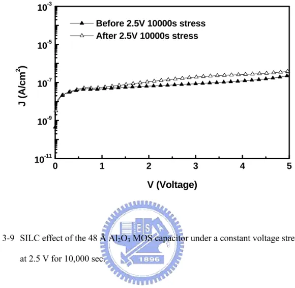
Fig. 3-8 Current density changes of the 48 Å Al2O3 MOS capacitor under a constant
voltage stress at 2.5V for 1000sec.
Fig. 3-9 SILC effect of the 48 Å Al2O3 MOS capacitor under a constant voltage
stress at 2.5V for 10,000sec.
Fig. 3-10 Voltage changes of 48 Å Al2O3 MOS capacitor under a 0.1mA/cm2 current
density stress for 1000s.
Fig. 3-11 SILC effect of 48 Å Al2O3 MOS capacitor under a 0.1mA/cm2 current
density stress for 1000sec.
Fig. 3-12 J-V characteristics for Al2O3 (9.6 & 16.5 Å EOT)and La2O3 (4.8 Å EOT)
capacitors. Stacked structure is adopted to reduce leakage current for Dit
measurement.
Fig. 3-13 Cross-section TEM of Al2O3 and La2O3. Very smooth interface is due to the
high thermal stability and native oxide free surface. Both dielectrics are amorphous.
Fig. 3-14 Cumulative distribution of leakage current and breakdown field for Al2O3
and La2O3 gate dielectrics.
Fig. 3-15 Hysteresis curves for Al2O3 and La2O3 gate dielectrics.
Fig. 3-16 Interface state density of Al2O3 and La2O3 on Si. Min Dit of 3x10¹⁰
eV-1/cm2 is obtained for both dielectrics and close to SiO 2/Si.
Fig. 3-17 Id-Vd characteristics of 30mmx1200mm NMOSFETs with 33 Å La2O3 gate
dielectric.
Fig. 3-18 Subthreshold characteristic and transconductance for 33 Å La2O3
NMOSFETs as a function of gate bias.
Fig. 3-19 Effective electron mobility versus electrical field for 33 Å La2O3
nNMOSFET.
C/cm2 for respective La
2O3 and Al2O3.
Fig. 3-21 Stress induced leakage current and current variation for Al2O3 and La2O3
under -2.5V for 1hr.
Fig. 3-22 QBD distribution of La2O3 dielectricwith different Vg. For 50% MTTF and
Chapter 4
Fig. 4-1 The room temperature Ids-Vgs characteristics of NiSi/Al2O3 nMOSFETs
under double sweep measurements. The inserted figures are the enlarged view to show the hysteresis.
Fig. 4-2 The room temperature Ids-Vgs characteristics of NiGe/Al2O3 pMOSFETs
under double sweep measurements. The inserted figures are the enlarged view to show the hysteresis.
Fig. 4-3 The room temperature C-V characteristics of NiSi/Al2O3 nMOS capacitors
under double sweep measurements. The inserted figures are the enlarged view to show the hysteresis.
Fig. 4-4 The room temperature C-V characteristics of NiGe/Al2O3 pMOS capacitors
under double sweep measurements. The inserted figures are the enlarged view to show the hysteresis.
Fig. 4-5 The Ids-Vgs changes of NiGe/Al2O3 pMOSFETs stressed at 85oC and 10
MV/cm for 1 hour.
Fig. 4-6 The ∆Vt changes of NiGe/Al2O3 pMOSFETs stressed at 85oC and 10
MV/cm for 1 hour. For comparison, the data from poly-Si/SiON and TaN/HfAlO (from reference 6) are also added under the same stress condition.
Fig. 4-7 The Ids-Vgs change of NiSi/Al2O3 nMOSFETs stressed at 85oC and 10
MV/cm for 1 hour.
Fig. 4-8 The ∆Vt changes of NiSi/Al2O3 nMOSFETs stressed at 85oC and 10
MV/cm for 1 hour. For comparison, the data from poly-Si/SiON and TaN/HfAlO (from reference 6) are also added under the same stress condition.
Fig. 4-9 The extrapolated maximum operation voltage for 10 years lifetime of NiSi/Al2O3 nMOSFETs and NiGe/Al2O3 pMOSFETs under failure
condition of 50 mV change in Vt at 85oC. The data from oxynitride is also
Chapter 5
Fig. 5-1 The J-(VG-VFB) characteristics of MOS capacitors with 42 Å Al2O3 gate
dielectric (19 Å EOT) with or without Cu contamination. The MOS devices with 30 Å thermal SiO2 are also added for comparison. The devices were
contaminated by 10 ppb or 10 ppm Cu.
Fig. 5-2 The distribution of leakage current density for (a) 42 Å Al2O3 gate
dielectric (19 Å EOT), (b) 30 Å thermal SiO2 and (c) 36 Å SiON with
23%N content (30 Å EOT) gate dielectrics with or without Cu contamination.
Fig. 5-3 The (a) QBD and (b) tBD distribution of 42 Å Al2O3 gate dielectric (19 Å
EOT) MOS devices under different Cu contamination level. The distributions of 30 Å SiO2 MOS capacitors with or without Cu
contamination are also added for comparison.
Fig. 5-4 The stress effect on J-(VG-VFB) characteristics for MOS capacitors
contaminated by Cu with (a) 42 Å Al2O3 gate dielectric (19 Å EOT) and (b)
30 Å SiO2. The applied stress condition is at –3.3 V for 10,000 sec.
Fig. 5-5 The stress and Cu contamination effect on ∆J/J-V characteristics of (a) 42 Å Al2O3 gate dielectric (19 Å EOT) and (b) control 30 Å SiO2 MOS
Table Caption
Chapter 1
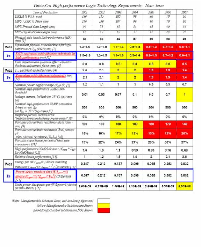
Table 1-1 The International Technology Roadmap of ITRS for Semiconductor 2002. Table 1-2 Physical properties for various high-k materials.
Chapter 1
Introduction
1.1
Background and Motivation of Al
2O
3High-k Dielectric
Continual the scaling-down of MOS devices has to a constant reduction of the thickness of the gate dielectrics. For sub-0.13 um gate length technologies, an equivalent SiO2 thickness lower than 15 Å is required. MOS transistor with gate oxide
thickness of 15 Å and 13 Å has been demonstrated, respectively [1.1], [1.2]. Nevertheless, silicon dioxide does not satisfy all criteria for an ideal technological insulator, such a low thickness would subjected to several problems for conventional dielectrics, such as silicon oxide, silicon nitride or oxynitride films, in terms of leakage current density and resistance to impurity diffusion. Thereby reducing the thickness with lower leakage current and high resistance to impurity diffusion plays an important role. A solution is to replace these materials by high dielectric constant (high-k) insulators, thus allowing an increase of the packing density without a further reduction of the insulator thickness. Fig. 1-1 shows ITRS projections for low power gate leakage. Actually, novel high-k gate dielectric has been identified in future R & D plan [1.3] as one of the most important factors for deca-nano CMOS technology.
thickness of gate oxide have be below 13 Å after 2005, and the use high constant dielectrics as insulator to replace SiO2 has become so widespread in the future gate
dielectric. It would seem almost unchangeable [1.4]. Since the leakage current is related to the physical thickness, the increasing thickness can reduce the gate leakage current of the devices. Although high-k dielectric films exhibit smaller band gap, weak bond, and charge trapping than SiO2. The high-k dielectric films with the same
effective oxide thickness (EOT) with SiO2 provide sufficient gate control with reduce
gate leakage. That is the reason why high-k dielectrics have drawn much attention for future gate dielectrics.
Recently, many high-k dielectric candidate materials have widely investigated and the characteristics and issues of those materials have also been reported. Table 1-2 shows the physical properties for various high-k materials. The high-k dielectrics show good performances are always accompanied by other drawbacks. Finding out the most suitable high-k dielectric for device and altering the device structure or process to meet the requirement of the high speed device are significant tasks to implant high-k dielectrics to the next VLSI generation. Many alternatives to SiO2
have been proposed. Silicon nitride (Si3N4) is an attractive candidate for this purpose
due to its higher dielectric constant (~7). However, Si3N4 has a poor interface with
trap density in the film. Therefore, it is not an attractive candidate for a future gate dielectric for ULSI [1.5].
Among the high-k simple metal oxide, such as Tantalum oxide (Ta2O5) and
Titanium oxide (TiO2) are seriously considered as candidates for advanced CMOS
gate dielectric applications. Because of they exhibit the merits including the better capacitance linearity than that SiO2, the lower process temperature and the larger band
gap (4.65eV) than that of the other high-k dielectrics and high reliability [1.6], [1.7]. However, Ta2O5 and TiO2 are not thermally stability when directly contacted to Si
substrate [1.8]. They react with Si and form an interfacial low-k dielectric layer. Additional barrier layer has been used to prevent the reaction, but it increases equivalent oxide thickness (EOT) and process complexity [1.9]. In addition, crystallization will cause from post implant RTA.
Recently, HfO2 and ZrO2 have attracted much attention due to their thermal
stability with poly or TiN and TaN [1.10], [1.11], [1.12]. In addition, they also exhibits suitable dielectric constant (25~30) and energy band gap, for the use of MOSFET in sub-micron generation. However, HfO2 is poor barrier to oxygen diffusion, oxygen
tends to diffuse though HfO2 and form oxide interlayer after high temperature process
and it becomes difficult to achieve the effective oxide thickness below 15 Å. Furthermore, it exists an important issue for the integration of HfO2 and ZrO2. The
boron penetration effect is severe when single HfO2 serves as gate dielectric of
transistors, while ZrO2 reacts with poly silicon to form Zr silicide after post implant
annealing. This Zr-silicide defects increase the leakage current and degrade the reliability. Besides, both HfO2 and ZrO2 will crystallize at the temperature higher than
500oC. After source/drain activation, this property increases the leakage current and
power dissipation of the device.
The use of aluminum oxide (Al2O3) has attracted much attention because it has
some advantage over silicon dioxide (SiO2) which makes it promising; lower leakage
current, greater resistance to ionic motion, greater radiation hardness, the possibility of obtaining low threshold voltage MOSFETs, and possibility of use in nonvolatile memory devices. Balk [1.13] has proposed a set of criteria to be employed in the selection of insulators either instead of, or in conjunction with silicon dioxide (SiO2) :
(1) high dielectric constant, (2) high breakdown strength, (3) an effective barrier against contaminants such as alkali ions, copper and moisture, (4) etchable in liquid etchants at or near room temperature, (5) stable electrical properties when used as gate dielectric in MOSFET, (6) controllable electrical properties when used as nonvolatile memory elements. Al2O3 fulfills many of these requirements very well. Al2O3 is
believed to be more resistant to ion penetration than silicon dioxide (SiO2). Besides,
and memory application.
1.2 The Formation of Al
2O
3High-k Dielectric
Many methods to deposit ultra thin high-k dielectrics on substrates have been proposed in recent years and various methods exhibit the merits as well as some other issues that have to be solved.
In this study, we used the advance deposition method to fabricate Al2O3 high-k
dielectrics. We utilized the self-limit property of Al2O3 to prevent from the formation
of interface oxide and have the effect of aluminum doping at the same time. The pre-cleaned wafer was loaded in the chamber under high vacuum condition, and then aluminum layer was deposited in evaporation on Si Substrate. Because extremely high quality is required for gate dielectric, we have used thermally grown Al2O3 from
oxidized Al on Si-substrate. In comparison, sputtering and oxygen plasma have been used in the past to deposit aluminum oxide. However, high defects can be expected from Ar-ion bombardment and oxygen plasma respectively [1.14]. The MOS transistor and capacitor devices with Al2O3 dielectrics are fabricated and measured. It
is found in our study that the self-limiting oxidation mechanism is one of the important merits of Al2O3 for either reproducibility or uniformity control. We have
first characterized the electrical property of Al2O3 as dielectric of MOS-capacitor to
applied it to be gate dielectric of a MOSFET and characterized its electrical properties.
1.3 The Measurement of the Devices
To investigate the electrical characteristics of MOSFETs, we measured the leakage current, stress induced leakage current and Vt degradation using HP4156C
semiconductor parameter analyzer with high temperature chuck. Besides, HP4284A precision LCR meter was used to evaluate the capacitance at a high frequency 100KHz and a quasi-static frequency 10Hz. The thickness of the aluminum oxide film was measured by a single wavelength ellipsometer. We assumed the oxide layer was homogeneous with a refractive index n=1.76 (typical of bulk aluminum oxide). The structure and atomic composition of capacitor samples were investigated by micro analyses, such as secondary ion mass spectrometry (SIMS). For the SIMS analysis, we can determine the oxide and aluminum diffusion profile into silicon. The leakage current of 48 Å Al2O3 as dielectric of MOS-capacitor is already better than that of
SiO2 with the same equivalent thickness of 13 Å. Capacitance-Voltage (C-V) curve
shows its higher dielectric constant (k). Besides, the effective mobility of Al2O3 gate
MOSFETs is closed to the effective mobility of traditional SiO2 gate MOSFETs. The
show the high quality of Al2O3 dielectric according to its reliability analysis.
Capacitor reliability tests were carried out by measuring constant current stress, constant voltage stress and SILC (Stress Induced Leakage Current) effect. To investigate the Bias-Temperature Instability (BTI) effects on fully silicided-gate/Al2O3
CMOSFETs. The ∆Vt changes have measured after 10MV/cm and 85oC stress. The 10
years lifetime Vmax-10years is from the extrapolation of ∆Vt changes at high gate voltage
and high temperature. Furthermore, to characteristics the Cu contamination effect on Al2O3 gate dielectric, we measured the gate dielectric leakage current,
charge-to-breakdown and stress-induced leakage current on Al2O3 and SiO2,
respectively. These results suggest the possible application of aluminum oxide (Al2O3)
to the next generation of VLSI.
1.4 Thesis Outline
In this thesis, we performed a high-k dielectric Al2O3 for the MOSFETs device
by thermal oxidizing the thin Al and than studied the electrical properties and mechanism of Al2O3 dielectric. Moreover, we have studied the Bias-Temperature
Instability (NBTI) on fully Nickel silicide (NiSi) and germanided (NiGe) gate on high-k Al2O3 nMOSFETs and pMOSFETs, respectively. Finally, the Cu contamination
In Chapter 2, we have studied the Al2O3 to use as an alternative gate dielectric.
To ensure good quality, Al2O3 is thermally oxidized from MBE-grown AlAs or Al on
Si-substrates. Experimental results indicate that the leakage current from oxidized AlAs is larger than that from directly oxidized Al, which may be due to the weak As2O3 inside Al2O3. The leakage current of a 53 Å Al2O3 is already lower than that of
SiO2 with an equivalent oxide thickness of 21 Å.
In Chapter 3, firstly we have reported a very simple process to fabricate Al2O3
gate dielectric with k (9.0 to 9.8) greater than Si3N4. Al2O3 is formed by direct
oxidation from thermally evaporated Al. The 48 Å Al2O3 has ~6 orders lower leakage
current than equivalent 13 Å SiO2. Good Al2O3/Si interface was evidenced by the low
interface density of 1x10¹¹ eVcm-2 and compatible electron mobility with thermal
SiO2. Good reliability is measured from the small SILC after 2.5 V stress for 10,000s.
Secondly high quality La2O3 was fabricated with EOT of 9.6 Å, leakage current of 0.4
A/cm2 and D
it of both 3x10¹⁰ eV-1/cm2. The high-k is further evidenced from high
MOSFET’s Id and gm with low Ioff. Good SILC and QBD are obtained and comparable
with SiO2. The low EOT is due to the high thermodynamic stability in contact with Si
and stable after H2 annealing up to 550oC.
In Chapter 4, we have studied the Bias-Temperature Instability (BTI) on fully Nickel silicided (NiSi) and germanided (NiGe) gate on high-k Al2O3 nMOSFETs and
pMOSFETs, respectively. At an equivalent-oxide thickness (EOT) of 17 Å, the NiSi/Al2O3 pMOSFETs and NiGe/Al2O3 nMOSFETs have comparable threshold
voltage (Vt) change of -34 and 33 mV at 85oC and 10 MV/cm stress for 1 hour. This
result is quite different from the more severe native BTI (NBTI) degradation measured in oxynitride pMOSFET than positive BTI (PBTI) in nMOSFET. The extrapolated maximum voltage for 10 years lifetime is 1.16 and -1.12 V from NiSi-NiGe/Al2O3 CMOSFETs that can barely meet the required 1 V operation with
10% safety margin. However, further improvement is still required since the 18 Å oxynitride CMOSFETs have higher 10 years lifetime operation voltage of 2.48 and -1.52 V for PBTI and NBTI, respectively.
In Chapter 5, we have studied the Cu contamination effect on 42 Å thick Al2O3
MOS capacitors with an equivalent-oxide thickness (EOT) of 19 Å. In contrast to the large degradation of gate oxide integrity of control 30 Å SiO2 MOS capacitors
contaminated by Cu, the 19 Å EOT Al2O3 MOS devices have good Cu contamination
resistance with only small degradation of gate dielectric leakage current, charge-to-breakdown and stress-induced leakage current. This strong Cu contamination resistance is similar to oxynitride (with high nitrogen content) but the Al2O3 gate dielectric has the advantage of higher-k value and lower gate dielectric
Fig. 1-1 ITRS projections for low power gate leakage.
Material Dielectric constant (k) Band gap Eg(eV) ∆Ec (eV) to Si Contact stability with Si (KJ/mole) Si+Mox--> M+ SiO Crystal structure
SiO2 3.9 8.9 3.2 Stable Amorphous
Al2O3 9 8.7 2.8 63.4 Amorphous La2O3 30 4.3 2.3 98.5 Amorphous HfO2 25 5.7 1.5 47.6 Crystal T>700C ZrO2 25 7.8 1.4 42.3 Crystal T>400~800C TiO2 80 3.5 1.2 - Tetragonal
Chapter 2
Electrical characterization of Al
2O
3on Si from
thermally oxidized AlAs and Al
2.1 Introduction
It has been shown that the practical scaling limit for gate oxide is due to the leakage current by direct-tunneling process [2.1], although 11-15 Å direct-tunneling gate oxide has already been demonstrated [2.2], [2.3]. The thickness of thermally grown gate oxide is scaled down to 35-40 Å for the 0.18-µm VLSI generation, and further scaling down below 15 Å is required within a few years [2.4]. Unfortunately the large direct-tunneling current precludes the use of silicon dioxide (SiO2) below
15-20 Å thickness. However, continuously scaling down the gate oxide is necessary to increase the current drive capability of MOSFETs and the operation speed of ICs. The relationship of drive current and gate oxide thickness is shown in equation (1):
IDsat=1 2
µ
n tox KA 0 L Wε (VG-VT) 2 (1)where IDsat is the device saturation current, VG is the applied gate voltage and k is
the dielectric constant of gate capacitor. The only solution to overcome this difficulty and to continuously scale down the gate dielectric is to use a thicker dielectric with a higher k value. Therefore novel high-k gate dielectric has been identified as one of the
most important R & D plans [2.4] for deca-nano CMOS technology. Unfortunately, because of the stringent requirements for device quality gate dielectric, no satisfactory alternatives to SiO2 has so far been found. Recently, aluminum oxide (Al2O3) has
attracted much attention because of its very high dielectric constant (~10) that can be used for next generation DRAM and Flash memory application [2.5]. Moreover, Al2O3 has also been treated as a gate barrier in InAlAs/InGaAs MESFET using
plasma oxidation of deposited Al [2.6]. In this study, we have first characterized the electrical property of Al2O3 to use as an alternative gate dielectric of MOSFETs.
Because extremely high quality is required for gate dielectric, we have used thermally grown Al2O3 from oxidized AlAs or Al that were grown in an ultra-high vacuum
molecular beam epitaxy (MBE) system. In comparison, sputtering deposition and O2
plasma oxidation have been used in the past to deposit Al2O3; however high defects
can be expected from Ar+ bombardment and plasma damage, respectively. In this
work, the leakage current of a 53 Å Al2O3 from direct oxidized Al is already better
than that of SiO2 with the equivalent thickness of 21 Å [2.2]. This result suggests the
possible application of Al2O3 to VLSI.
2.2 Experimental
this study. After modified RCA cleaning, HF dipping, rinsing in DI water and spun dry, the wafer was treated by HF-vapor passivation and immediately loading into the MBE chamber. The HF-vapor passivation has been used to reduce thermal budget to desorb the native oxide [2.7]. Then 40-80 Å AlAs or 40-55 Å Al were grown by MBE at 500oC. The oxidation process was performed in a standard furnace at 500oC for 90
min., and the dielectric thickness was measured by an ellipsometer. After oxidation, 3000 Å poly-Si was deposited followed by phosphorus doping using POCl3 at 850oC.
The wafers were then received a 30-min. nitrogen anneal at 800oC. This anneal was
found to be very effective to reduce dielectric leakage current. Subsequently, 3000 Å Al was deposited and gate electrode was defined by patterning and wet etching. The gate dielectrics were electrically characterized by I-V leakage current using a semiconductor parameter analyzer, and the composition profiles were measured using secondary ion mass spectroscopy (SIMS).
2.3 Results and Discussion
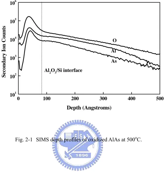
Fig. 2-1 presents the SIMS profiles of oxidized AlAs at 500oC, where O, Al and As are detected within the oxidized layer. The possible AlAs oxidation process is in the following equation:
Therefore both Al2O3 and As2O3 are formed during AlAs oxidation. As shown in Fig.
2-1, significant Al and As diffusion into Si is observed. The diffused As into Si will behave as a n-type dopant and change the threshold voltage, while the amount of diffused Al is dependent on the solid solubility of Si. However, none of these effects are desirable for MOS devices. The reduced surface concentration of As is due to the out-diffusion into ambient during oxidation.
Fig. 2-2 shows the SIMS profile of oxidized Al. The O2 concentration decreases
to its background value as increasing depth beyond the oxidized layer. This is because the Si oxidation rate is negligibly slow at this temperature. In sharp contrast to AlAs oxidation, the oxidized Al shows a much sharper SIMS profiles. Possible reason may be due to the absence of As-enhanced diffusion during oxidation. Another advantage of direct Al oxidation may be due to the strong bonding energy of Al2O3 instead of
As2O3 from oxidized AlAs. Therefore, the oxidized Al films may provide not only
better material quality but also lower diffusion into Si during oxidation.
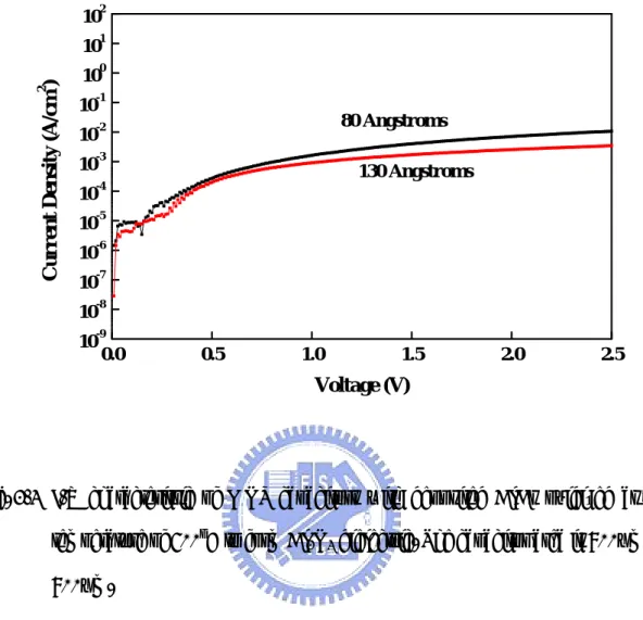
We have further characterized the electrical behavior of these oxides. Fig. 2-3 shows the typical J-V characteristics of MOS capacitors from oxidized AlAs. The capacitor leakage current reduces with increasing dielectric thickness from 80 to 130 Å. This is a typical behavior because a thicker insulating barrier has lower electric field that can block the electron transport more easily. However, this thicker insulating
barrier did not successfully reduce the leakage current at low voltages less than ~0.7 V. Possible reasons may be due to trap-assisted tunneling at low electric field [2.8]. The traps may be generated by the weak bonding strength of As2O3 inside Al2O3 matrix or
vacancies by As out-diffusion.
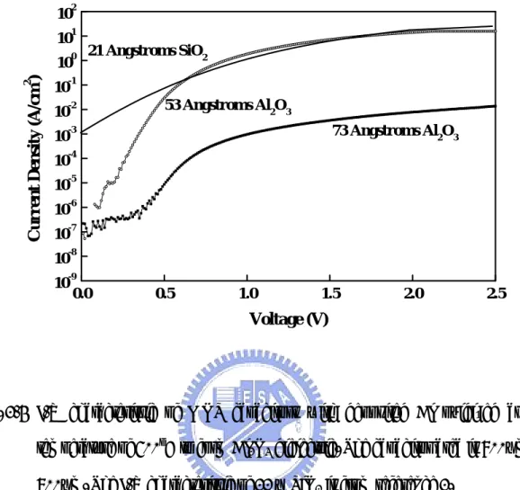
To investigate the effect of As-related weak As2O3 or vacancies, we have studied
the electric characteristic of capacitors with directly oxidized Al. In comparison the J-V characteristics of ~ 80 Å oxides in Figs. 2-3 and 2-4, a much lower leakage current is observed at gate voltage below 1 V from directly oxidized Al. This leakage current at low gate electric field is related to the intrinsic defects [2.8] that is similar to stress-induced leakage current (SILC) [2.7], [2.9]. Therefore the As-related weak As2O3 or vacancies are responsible to the increased oxide leakage current. The almost
same current at high voltages is due to the dominated tunneling mechanism. We have further compared the leakage current of Al2O3 with SiO2 from the published I-V
characteristic [2.2]. It is important to note that the leakage current of 53 Å Al2O3 is
already better than the leakage current of MOS capacitors with the same equivalent thickness of 21 Å thick SiO2 [2.2].
2.4 Conclusion
We have studied the thermally oxidized AlAs and Al to use as an alternative gate dielectric. The leakage current from AlAs oxidation is larger than that from Al
oxidation at low voltages. The leakage current of a 53 Å Al2O3 is already lower than
SiO2 with an equivalent oxide thickness of 21 Å. These results suggest that scaling
Fig. 2-1 SIMS depth profiles of oxidized AlAs at 500oC. 0 100 200 300 400 500 101 102 103 104 105 106 Al2O3/Si interface As Al O Secondary Ion C o unts Depth (Angstroms)
Fig. 2-2 SIMS depth profiles of oxidized Al at 500oC. 0 100 200 300 400 500 101 102 103 104 105 106 Al2O3/Si interface Al O Secondary Ion C o unts Depth (Angstroms)
Fig. 2-3 J-V characteristic of MOS capacitors with deposited AlAs oxidized at a temperature of 500oC to form Al2O3 dielectric. The capacitor area is 800µm×
800µm. 0.0 0.5 1.0 1.5 2.0 2.5 10-9 10-8 10-7 10-6 10-5 10-4 10-3 10-2 10-1 100 101 102 130 Angstroms 80 Angstroms C urrent D ensi ty ( A /c m 2 ) Voltage (V)
Fig. 2-4 J-V characteristic of MOS capacitors with deposited Al oxidized at a temperature of 500oC to form Al
2O3 dielectric. The capacitor area is 800µm×
800µm. The J-V characteristic of 21 Å SiO2 is from reference 2.
0.0 0.5 1.0 1.5 2.0 2.5 10-9 10-8 10-7 10-6 10-5 10-4 10-3 10-2 10-1 100 101 102 21 Angstroms SiO2 53 Angstroms Al2O3 73 Angstroms Al2O3 C urrent D ensi ty ( A /c m 2 ) Voltage (V)
Chapter 3
Device and Reliability of High-k Al
2O
3and La
2O
3Gate Dielectric with Good Mobility and Low D
it3.1 Introduction
By continuously scaling down the CMOS technology, ultra-thin high-k gate dielectrics with low leakage current are required to replace the direct-tunneling current dominated thermal SiO2. Recently Si3N4 gate dielectric has been studied
extensively to replace thermal SiO2 [3.1]; however, the marginal improvement beyond
SiO2 is due to the relatively lower k and slightly higher leakage current. Although
stacked high-k materials have been studied to achieve higher k value than that of Si3N4 [3.2], [3.3], it may require complicated process steps and the leakage current is
still higher than expected. In this study, we report a very simple process to fabricate Al2O3 as an alternative gate dielectric with a k value (9.0 to 9.8) greater than Si3N4. To
avoid any process related damage, Al2O3 gate dielectric is formed by direct oxidation
from thermally evaporated Al. In addition to high-k, the 48 Å Al2O3 has ~6 orders
lower leakage current than equivalent 13 Å SiO2. Good mobility, interface trap density,
and reliability are also achieved using this process.
reduction of EOT may be limited by the interface reaction region between high-k material and Si [3.4], [3.5]. Therefore, the search for thermodynamically stable high-k dielectric directly on Si is important to meet future sub-10 Å requirement. Besides the required good electrical properties such as low interface trap density (Dit), low
leakage current, high breakdown field (EBD) and good reliability, high-k material must
also be compatible with existing VLSI process. Thus, good stability with H2 and high
transition temperature from amorphous to crystal [3.5] are necessary to prevent dielectric degradation by H2 and crystalline structure created defects or dislocations
during strain relaxation in process. Previously, we have worked that amorphous Al2O3
directly on Si can meet near all the requirements and stable up to 1000oC [3.6], except
that EOT (21 Å) and Dit (1x10¹¹ eV-1/cm2) are still high. The high Dit is unacceptable
for IC because of the increased noise [3.7]. In this study, we have used amorphous La2O3 (k~27) to achieve 4.8 Å EOT and reduced Al2O3 EOT to 9.6 Å, where La2O3
has similar property as Al2O3 but with even better thermal stability on Si (Table 1-2).
In addition to respective low leakage current of 0.06 and 0.4A/cm2 for La
2O3 and
Al2O3,both dielectrics now have good Dit (3x10¹⁰ eV-1/cm2), EBD, SILC, and QBD as
compared with SiO2.
3.2.1 Experimental
To avoid any possible process-related damage in Al2O3 gate dielectric [3.8], we
have used direct thermal oxidation from thermally evaporated Al on Si. Native oxide is suppressed by a HF-vapor passivation and desorbed in-situ inside an ultra-high vacuum MBE environment [3.9], followed by an immediate Al evaporation. Deposited Al was oxidized at a temperature of 400oC to form Al
2O3. Then the Al2O3
was annealed in nitrogen ambient to reduce defects. Poly-Si gate MOS capacitor and transistor were fabricated to evaluate the electrical characteristics. The suppression of native oxide is important to achieve higher k in Al2O3, and we have used similar idea
to achieve atomically smooth ultra-thin oxide with good electrical characteristics and reliability [3.10]. For comparison, MOS capacitor and transistor were also fabricated by thermal SiO2.
3.2.2 Results and Discussion
3.2.2.1 The physical property of Al
2O
3We have first measured the SIMS profile in Fig. 3-1 to confirm the formation of Al2O3. Although Al diffusion into Si can be observed, the concentration reduces
observed in Al2O3 bulk oxidized at 500oC. We have also used C-V measurement to
determine the Al diffusion and the concentration is lower than 1x1016 cm-3.
Furthermore, the field-dependent mobility also suggests the low Al diffusion into Si.
3.2.2.2 Gate capacitor
Fig. 3-3 presents the J-V characteristic of a 48 Å Al2O3 capacitor. The leakage
current is ~6 orders of magnitude lower than that of the equivalent 13 Å thermal SiO2.
In order to obtain an accurate k value, we have also measured the C-V of a thick 110 Å Al2O3 capacitor. As shown in Fig. 3-4, a k value of 9.0 is measured that is higher
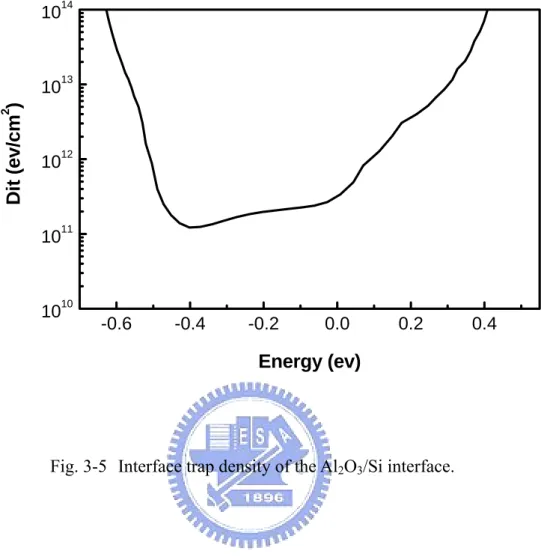
than Si3N4. In Fig. 3-5 presents the measured interface trap density with a mid-gap
value of 1x10¹¹ eVcm-2 from this capacitor. This low interface trap density is suitable
for MOSFET application.
3.2.2.3 Mobility and transistor performance
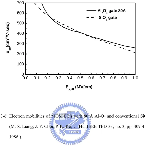
To further characterize the Al2O3/Si interface, we have fabricated a wide gate
MOSFET to measure the electron mobility. Fig. 3-6 shows the effective mobility of an 80 Å Al2O3 MOSFET. The electron mobility is comparable to published mobility data
than that of thermal SiO2 also proves the high-k value in Al2O3 MOSFET and a k of
9.8 is obtained.
3.2.2.4 Reliability
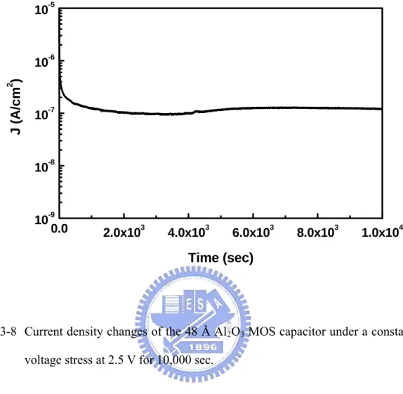
Fig. 3-8 and Fig. 3-9 show the 48 Å Al2O3 gate dielectric under a 2.5 V constant
stress for 10,000 sec, and good reliability is evidenced from the very small current change and stress-induced leakage current (SILC) respectively. Fig. 3-10 and Fig. 3-11 present the same Al2O3 gate dielectric under a much higher stress of ~5.4 V with
a 0.1 mA/cm2 constant current density for 1000 sec. The small voltage changes less
than 0.04 V and the small SILC also suggest the excellent reliability. Therefore, the Al2O3 gate dielectric is suitable for continuously operation at VLSI generations of 2.5
V and beyond.
3.3 Device and Reliability of High-k La
2O
3Gate Dielectric
3.3.1 Experimental
To avoid any k value reduction, interfacial native oxide is suppressed by HF-vapor passivation and in-situ desorption [3.6] followed by an immediate La or Al evaporation. Because La or Al is highly reactive with O2, low oxidation temperatures
≤ 400oC is used to reduce metal diffusion into Si. The formed oxides were further
annealed in N2 at 900oC. To reduce gate depletion, Al gate is used for MOS capacitor
and transistor to evaluate the electrical characteristics. H2 annealing at 450-550oC is
performed to study the stability withH2. Besides achieved higher k, suppression of
native oxide is important to obtain a smooth interface, low Dit, and high reliability in
our previously achieved atomically smooth ultra-thin oxides.
3.3.2 Results and Discussion
3.3.2.1 Gate capacitor
Fig. 3-12 presents the J-V characteristics of La2O3 and Al2O3 capacitors.
Comparable leakage current for La2O3 on Si or Si0.3Ge0.7 I s obtained that is important
for high mobility PMOS [3.11]. The stacked Al2O3/La2O3 is used to reduce leakage
current for C-V to obtain Dit. In order to get accurate k and EOT, the oxide thickness
is carefully examined by both ellipsometer and TEM in Fig. 3-13. The very uniform oxide and smooth interface are due to native oxide free surface and high thermal stability in Table 1-2 as contact with Si. Therefore, low EOT can be expected. Fig. 3-14 shows the cumulative values for high-k oxides, and leakage current of 0.06 A/cm2 for La
4.8 Å and 9.6 Å EOT (without QM correction). Small hysterisis of 11 and 22 mV are measured for respective dielectrics that indicates good quality because of applied high annealing temperature without transition to crystal structure [3.5]. Fig. 3-16 shows the measured Dit of 3x10¹⁰ eV-1/cm2 from both capacitors. This low Dit close to thermal
SiO2 is extremely important for circuit to lower 1/f noise [3.7].
3.3.2.2 Transistor performance with 4.8 Å EOT
We have further fabricated wide gate MOSFETs with 4.8 Å EOT. Figs. 3-17 shows the device Id-Vd, and important Id-Vg and gm are plotted in Fig. 3-18. The very
high current drive and gm are due to high-k that gives a k of ~27 consistent with C-V
measurement. Good device pinch-off Ioff < 10-10A/µm and small sub-threshold swing
of 75 mV/decade are observed, and the small swing also suggests the low Dit. The
effective mobility is further plotted in Fig. 3-19. The electron mobility is comparable with published universal mobility data for thermal SiO2 because of low Dit.
3.3.2.3 Reliability
Fig. 3-20 shows the gate dielectrics under a -2.5 V constant stress for 1 hour with total Qinj of 1.3x10³ and 1.2x10⁵C/cm2 for La2O3 and Al2O3, respectively. No
significant charge trapping is occurred during stress, and small SILC for both dielectrics is observed in Fig. 3-21. Good reliability for 4.8 Å EOT La2O3 is
evidenced from the high QBD in Fig. 3-22 and comparable with current SiO2 [3.12].
The good SILC and QBD may be due to the high lattice energy in Table 1-2. From the
50% failure time, an extrapolated max voltage of 2.3 V is obtained for 10 years lifetime that suggests good reliability for VLSI application with 4.8 Å EOT and small leakage of 0.06 A/cm2 at 1 V.
3.4 Conclusion
We report a very simple process to fabricate Al2O3 gate dielectric with k (9.0 to
9.8) greater than Si3N4. Al2O3 is formed by direct oxidation from thermally
evaporated Al. The 48 Å Al2O3 has ~6 orders lower leakage current than equivalent 13
Å SiO2. Good Al2O3/Si interface was evidenced by the low interface density of 1x10¹¹
eVcm-2 and compatible electron mobility with thermal SiO
2. Good reliability is
measured from the small SILC after 2.5 V stress for 10,000 sec.
High quality La2O3 and Al2O3 are fabricated with EOT of 4.8 and 9.6 Å, leakage
current of 0.06 and 0.4 A/cm2 and D
it of both 3x10¹⁰ eV-1/cm2, respectively. The
Fig. 4-1
SIMS depth profile of oxidized Al at 500oC. The measured thickness is close to that measured by ellipsometer & cross-sectional TEM.0
100
200
300
400
500
10
110
210
310
410
510
6 Al2O3/Si interfaceAl
O
Se co nda ry I o n Co unt s Depth (Angstroms)(a)
(b)
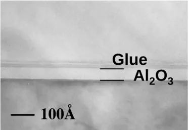
Fig. 3-2 TEM photos of Al oxidized at (a) 400oC and (b) 500oC.
Al
2
O
3
Glue
100Å
Al
2
O
3
Glue
100Å
Crystal
100Å
Crystal
100Å
0 1 2 3 4 5 6 7 8 10-11 10-9 10-7 10-5 10-3 10-1 101 103 105 48 A Al 2O3 13 A SiO 2
Jg (A/cm
2)
Vg (Voltage)
Fig. 3-4 C-V characteristics of 110 Å Al2O3 MOS capacitor. -2 -1 0 1 2 0 100 200 300 400 500 600 Capacitance (pF) V (Voltage)
Fig. 3-5 Interface trap density of the Al2O3/Si interface. -0.6 -0.4 -0.2 0.0 0.2 0.4 1010 1011 1012 1013 1014 Di t (ev/cm 2 ) Energy (ev)
0.0 0.1 0.2 0.3 0.4 0.5 0.6 0.7 0.8 0.9 1.0 0 100 200 300 400 500 600 700 Al2O3 gate 80A SiO2 gate u eff (cm 2 /V-s e c ) E s,eff (MV/cm)
Fig. 3-6 Electron mobilities of MOSFET’s with 80 Å Al2O3 and conventional SiO2.
(M. S. Liang, J. Y. Choi, P. K. Ko, C. Hu, IEEE TED-33, no. 3, pp. 409-413, 1986.).
Fig. 3-7 Id-Vd characteristics of an 80 Å Al2O3 MOSFET. The high current drive in Al2O3 gives a k value of 9.8. 0 1 2 3 4 5 0.000 0.001 0.002 0.003 0.004 0.005 Al2O3 VG from 0V~5V SiO2 VG from 0V~5V I D (A ) VD (Voltage)
Fig. 3-8 Current density changes of the 48 Å Al2O3 MOS capacitor under a constant
voltage stress at 2.5 V for 10,000 sec. 0.0 2.0x10³ 4.0x10³ 6.0x10³ 8.0x10³ 1.0x10⁴ 10-9 10-8 10-7 10-6 10-5 J (A/cm 2 ) Time (sec)
Fig. 3-9 SILC effect of the 48 Å Al2O3 MOS capacitor under a constant voltage stress at 2.5 V for 10,000 sec. 0 1 2 3 4 5 10-11 10-9 10-7 10-5 10-3 Before 2.5V 10000s stress After 2.5V 10000s stress J (A/cm 2 ) V (Voltage)
Fig. 3-10 Voltage changes of 48 Å Al2O3 MOS capacitor under a 0.1 mA/cm2 current
density stress for 1000 sec.
0 200 400 600 800 1000 0 1 2 3 4 5 6 V g (V oltag e) Time (Sec) -0.10 -0.05 0.00 0.05 0.10 ∆V Voltage Vo ltage Chan ge ∆ V ( V ol ta ge)
Fig. 3-11 SILC effect of 48 Å Al2O3 MOS capacitor under a 0.1 mA/cm2 current
density stress for 1000 sec.
0 1 2 3 4 5 10-11 10-10 10-9 10-8 10-7 10-6 10-5 10-4 10-3
Before 0.1mA/cm2 stress 1000s After 0.1mA/cm2 stress 1000s
J (A/cm
2 )
Fig. 3-12 J-V characteristics for Al2O3 (9.6 & 16.5 Å EOT)and La2O3 (4.8 Å EOT)
capacitors. Stacked structure is adopted to reduce leakage current for Dit
measurement. 0 -1 -2 -3 -4 -5 -6 -7 -8 -9 10-9 10-7 10-5 10-3 10-1 101 103 EOT=4.8A 33A La2O3 on Si0.3Ge0.7 EOT=16.5A 36A Al2O3 on Si EOT=9.6A 21A Al2O3 on Si EOT=21.8A 36A Al2O3 / 33A La2O3 / Si EOT=4.8A 33A La2O3 on Si Gate Voltage (V) C u rre n t D e n s ity (A /c m 2 )
Fig. 3-13 Cross-section TEM of Al2O3 and La2O3. Very smooth interface is due to
the high thermal stability and native oxide free surface. Both dielectrics are amorphous. La2O3 Glue 10nm Glue Si Al2O3 Si
Fig. 3-14 Cumulative distribution of leakage current and breakdown field for Al2O3
and La2O3 gate dielectrics.
11 12 13 14 15 0 20 40 60 80 100 C u m u la ti v e F a ilu re (% ) Breakdown Field (MV/cm) 0.01 0.1 1 Al2O3 21A La2O3 33A
Fig. 3-15 Hysteresis curves for Al2O3 and La2O3 gate dielectrics. -3 -2 -1 0 1 2 0 100 200 300 400 500 600 700 800 Area=1x10⁻⁴ cm2 21A Al2O3 V △ FB=22mV 33A La2O3 V △ FB=11mV Gate Voltage (V) Capaci tance ( pF)
Fig. 3-16 Interface state density of Al2O3 and La2O3 on Si. Min Dit of 3x10¹⁰
eV-1/cm2 is obtained for both dielectrics and close to SiO2/Si.
-0.6 -0.5 -0.4 -0.3 -0.2 -0.1 0.0 0.1 0.2
1010
1011
1012
EOT=21.8A
EOT=16.5A 36A Al2O3 / 33A La2O3 / Si
36A Al2O3/Si D it (e v -1 /c m 2 ) Energy (ev)
Fig. 3-17 Id-Vd characteristics of 30 mm x 1200 mm nMOSFETs with 33 Å La2O3 gate dielectric. 0.00 0.25 0.50 0.75 1.00 1.25 1.50 1.75 2.00 0 5 10 15 20 25 Vg=0.75V Vg=0.6V Vg=0.45V Vg=0.3V Vg=0.15V Dr ai n Cur re n t ( m A) Drain Voltage (V)
Fig. 3-18 Subthreshold characteristic and transconductance for 33 Å La2O3
nMOSFETs as a function of gate bias.
0.0 0.2 0.4 0.6 0.8 1.0 1.2 1.4 1.6 1.8 2.0 10-6 10-5 10-4 10-3 10-2 10-1 SW=75 mV/decade Vd=0.4V Dr ai n Cu rr e nt ( A ) Gate Voltage (V) 0 5 10 15 20 25 30 35 40 g m ( m S /mm)
Fig. 3-19 Effective electron mobility versus electrical field for 33 Å La2O3 nMOSFET. 0.1 1 102 103 Eeff (MV/cm) u ef f (cm 2 /V -sec )
Fig. 3-20 Time evolution of Ig under -2.5 V for 1 hr with Qinj of 1.3x10³ and 1.5x10⁵
C/cm2 for respective La2O3 and Al2O3.
0 400 800 1200 1600 2000 2400 2800 3200 3600
10-1
100
101
102
33A La2O3 CVS under -2.5V for 3600sec
21A Al2O3 CVS under -2.5V for 3600sec
C u rre n t D e n s ity (A /c m 2 ) Time (second)
Fig. 3-21 Stress induced leakage current and current variation for Al2O3 and La2O3 under -2.5 V for 1hr. 0.0 -0.5 -1.0 -1.5 -2.0 -2.5 10-6 10-5 10-4 10-3 10-2 10-1 100 101 102 103 Cu rre n t D e ns ity (A /cm 2 ) 33A La2O3 21A Al2O3 Gate Voltage (V)
Solid Symbol: Fresh device Hollow Symbol: Stressed device
0 5 10 15 20 25 30 (I stres s ed - I F resh ) / I fre s h (% )
Fig. 3-22 QBD distribution of La2O3 dielectricwith different Vg. For 50% MTTF and
10 years lifetime, a max operation voltage of 2.3 V is obtained.
0 20 40 60 80 100 120 140 160 180 200 0 10 20 30 40 50 60 70 80 90 100 Vg=-3.3V Vg=-3.4V Vg=-3.5V Cu m u la tiv e Fa il u re (% ) QBD (C/cm2)
Chapter 4
Bias-Temperature Instability and Charge Trapping
on Fully-Silicided-Germanided Gates/High-k Al
2O
3CMOSFETs
4.1 Introduction
As continuous scaling down the MOSFET devices into sub-100 nm scale, oxynitride or metal-oxide high-k gate dielectric, with ultra-thin equivalent oxide thickness (EOT), is required to replace the conventional SiO2 to reduce gate dielectric
leakage current. To further increase the drive current in MOSFET, metal gate will be integrated with these high-k gate dielectrics [4.1]-[4.5]. However, one of the main concerns of such metal-gate/high-k MOSFETs is the poor Bias-Temperature Instability (BTI) [4.1], [4.6]-[4.8]. In particular, the negative BTI (NBTI) of pMOSFETs is becoming an increasingly serious problem of the CMOS reliability. It is known that the NBTI of oxynitride gate dielectric pMOSFETs is mainly related to nitrogen traps [4.9]-[4.12], hydrogen [4.13]-[4.14], moisture (H2O) [4.14], and
impurity diffusion [4.6] etc. Both the NBTI and positive BTI (PBTI) are even worse in metal-oxide high-k CMOSFETs than oxynitride devices [4.1], [4.6]-[4.8]. In this work, we have studied the BTI effect on fully silicided-germanided (NiSi-NiGe) dual
gates on high-k Al2O3 CMOSFETs [4.5], [4.15]-[4.19] and compared with a
benchmark oxynitride devices. The fully silicided gate has advantage of fully process compatible to current VLSI fabrication technology. The Al2O3 gate dielectric has
reasonable high-k and good thermal stability with amorphous type up to 1000oC [4.5],
[4.12], [4.15]-[4.21]. In contrast to the worse NBTI than PBTI in oxynitride devices, close NBTI and PBTI is found in fully NiSi-NiGe gates/Al2O3 CMOSFETs. At 17 Å
EOT, the extrapolated maximum operation voltage (Vmax-10years) for 10 years lifetime,
with 50 mV threshold voltage (Vt) change at 85oC, is 1.16 V and -1.12 V from PBTI
and NBTI, respectively. These results are comparable or better than the reported HfAlON [4.6] and HfSiON data [4.7]. The high Vmax-10years and close value for both
NBTI and PBTI may be due to the process without hydrogen and H2O that were used
during high-k HfAlON and HfSiON deposition by Atomic-Layer Deposition (ALD) using NH3 and H2O sources [4.6]. However, the inferior PBTI of NiSi-NiGe/Al2O3
CMOSFETs to oxynitride devices suggests that further improving the high-k dielectric quality is required.
4.2 Experimental
Standard n- and p-type (100) Si wafers with a typical resistivity of ~10 Ω-cm were used in this study. After standard cleaning, the device active region was formed
by thick field oxide and patterning. The source and drain region were implanted by 35 KeV Phosphorus or 25 KeV Boron for nMOSFETs or pMOSFETs respectively, followed by RTA activation. Then the ~39 Å Al2O3 was formed by physical-vapor
deposition, 400oC oxidation for 20 min. and 400oC annealing for 20 min. From the
C-V measurement, a k value of 8.9 and EOT of 17 Å were obtained. The slightly low-k value than bulk Al2O3 (k=10) is due to the oxidation of Si during post
deposition annealing. The fully NiSi and NiGe gates were formed by depositing 150 Å amorphous Si or Ge on Al2O3, 150 Å Ni for both n- and p-devices, and followed by
silicidation and germanidation at 400oC RTA for 30 sec [4.5], [4.15]-[4-19]. For
comparison, control oxynitride was formed by decoupled plasma nitridation [4.22] on a 18 Å SiO2 that was grown by oxygen at 700oC for 12 min. The formed oxynitride
has peak N concentration of 9% near poly gate interface, followed by post deposition annealing at 1000oC RTA. The fabricated CMOSFETs were further characterized by
C-V I-V, and Bias-Temperature (BT) measurements.
4.3 Results and Discussion
We have first measured the Ids-Vgs characteristics to examine the hysteresis
effects in Al2O3. Fig. 4-1 and Fig. 4-2 show the measured hysteresis on NiSi/Al2O3
nMOSFET, the double sweep of gate voltage from 0 to 1.5 V results in Vt shifted to
positive by +10 mV. This result suggests generating negative charge traps in nMOSFET. For pMOSFET, the double sweep of gate voltage from 0.5 to -1.5 V results in VT shifted to negative by -10 mV, which also indicates the generating
positive charge traps in bulk Al2O3 and Al2O3/Si interface. These amounts of charge
trappings may cause NBTI in pMOSFETs and PBTI in nMOSFETs. The poor Ioff in
nMOSFETs is due to the insufficient high temperature annealing (only 950oC RTA)
for ion-implanted damage. The limited RTA temperature also gives a relative poor sub-threshold swing because of the insufficient annealing of high-k dielectric defects. Further improving the leakage current and sub-threshold swing can be done by increasing RTA temperature to typical 1000-1050oC or using LaAlO
3 high-k dielectric
[4.24], [4.25].
We have also used the C-V to measure the hysteresis effects. Fig. 4-3 and Fig. 4-4 show the CV hysteresis characteristics, measured at 500 KHz, on NiSi/Al2O3
nMOSFETs and NiGe/Al2O3 pMOSFETs respectively, where conventional
bi-directional sweeps from inversion to accumulation were applied to these transistors. The double sweeping hysteresis of +10 mV and ~0 mV are measured for nMOS and pMOS capacitors, respectively. The smaller flat band voltage shift of pMOS capacitor than the Vt shifts of Ids-Vgs curves in NiGe/Al2O3 pMOSFETs may be due to the
relative slower and deeper traps that were unable to follow the AC signal [4.23]. Similar effect is also observed in other high-k dielectrics from quasi-static to RF frequency range [4.24]-[4.27].
Figs. 4-5 and Fig. 4-6 shows the NBTI characteristics of Ids-Vgs and Vt change
(∆Vt) for NiSi/Al2O3 pMOSFETs stressed at 10 MV/cm electric field and 85oC
ambient to 1 hour, respectively. This stress condition was chosen to compare with published data in the literature [4.6], [4.7]. For reference and comparison, the ∆Vt of
SiON pMOSFETs and the data of TaN/HfAlO [4.6] are also plotted in Fig. 4-6. After the 1 hour stress at 10 MV/cm and 85oC, a ∆Vt of -33 mV is measured suggesting that
the NBTI is one of the most serious reliability issues for fully NiSi gate/high-k Al2O3
pMOSFETs. The measured ∆Vt changes are comparable or better than the published
HfAlON [4.6], HfSiON [4.7] and HfTaO [4.1] where additional Al, N, Si or Ta must be added to HfO2 for BTI reliability improvement. However, the measured ∆Vt is still
larger than that of oxynitride devices with plasma generated N at top poly-Si/oxynitride interface. The possible reason of the inferior NBTI is due to the degraded interface of Al2O3/Si and bulk oxide change in Al2O3, where oxygen-riched
SiN interface on Al2O3 will be the possible solution for this important reliability issue
[4.10]-[4.12].
NiGe/Al2O3 nMOSFETs stressed at 10 MV/cm electric field and 85oC to 1 hour,
respectively. The ∆Vt of SiON nMOSFETs are also added in Fig. 4-8 for comparison.
After the 1 hour BT stress, a ∆Vt of 34 mV is measured for PBTI that is close to the
-33 mV value in NBTI. In sharp contrast, the NBTI of only 0.76 mV is measured in poly-Si/oxynitride (9% peak at poly-Si interface) nMOSFETs after the same BT stress that is lower than the 6.6 mV change in oxynitride pMOSFETs. The better PBTI than NBTI is normal for oxynitride MOSFETs where the mechanism is attributed to hole injection to break the H-Si bonds and created interface traps [4.9]-[4.14]. However, the measured NBTI and PBTI value are less than that of HfO2 [4.7], [4.8],
which may be due the strong A-O bond and consistent with the results in HfAlO [4.6]. The close PBTI and NBTI absolute value after BT stress in Al2O3 MOSFETs
suggesting the higher number of interface and bulk traps, which are normal for high-k gate dielectric, are the main causes and for larger ∆Vtchange than oxynitride
devices.
We have also measured BTI at other gate electric field for 10 years lifetime projection, where the lifetime at each gate voltage was defined by a ∆Vt=50 mV
change during stress. Such high gate voltage or electric field is especially required for poly-Si/SiON CMOS due to the excellent reliability. Figs. 4-9 show the time as a function of Vgs of nMOSFETs and pMOSFETs, respectively. The 10 years lifetime

![HPSH [ 氧化數平衡反應式係數 ]](data:image/gif;base64,R0lGODlhAQABAIAAAP///wAAACH5BAEAAAAALAAAAAABAAEAAAICRAEAOw==)