國 立 交 通 大 學
電 控 工 程 研 究 所
碩 士 論 文
具負載適應增益調適混合信號控制之邊界模式功
率因數修正交-直流轉換器
Design of a Load Adaptive Gain Adjustment
Mixed-Signal Critical Mode PFC AC-DC Converter
研 究 生:詹茗皓
指導教授:鄒應嶼 博士
具負載適應增益調適混合信號控制之邊界模式功
率因數修正交-直流轉換器
Design of a Load Adaptive Gain Adjustment
Mixed-Signal Critical Mode PFC AC-DC Converter
研 究 生:詹茗皓 Student: Ming-Hao Chan
指導教授:鄒應嶼 博士 Advisor: Dr. Ying-Yu Tzou
國立交通大學
電控工程研究所
碩士論文
A Thesis
Submitted to Institute of Electrical and Control Engineering College of Electrical Engineering
National Chiao-Tung University in Partial Fulfillment of the Requirements
for the Degree of Master in
Electrical Engineering October 2009
Hsinchu, Taiwan, Republic of China
具 負 載 適 應 增 益 調 適 混 合 信 號 控 制 之 邊 界 模 式 功 率
因 數 修 正 交 -直 流 轉 換 器
研究生:詹茗皓 指導教授:鄒應嶼 博士 國立交通大學電控工程研究所 中文摘要 本論文研製具負載適應增益調適混合信號控制之邊界模式功率因數修正 (critical-mode power-factor-correction, CRM PFC)交-直流轉換器,可應用於中低功率 電子設備如:可攜式電子產品或照明設備。本文所研製的混合信號控制其中電流迴 路使用類比方式實現,電壓迴路則以數位方式實現。本文並提出負載適應增益調 適(load adaptive gain adjustment)以及帶拒濾波器(notch filter)於數位電壓迴路,使系 統 輸 出 電 壓 可 達 到 最 佳 動 態 特 性 且 仍 可 使 輸 入 電 流 具 備 低 總 諧 波 失 真 (total-harmonic-distortion, THD)以及高功率因數(power-factor, PF)。在類比電流迴路 中,類比電流比較器為抑制雜訊的影響會加入磁滯比較區間 (hysteresis band),但 是磁滯比較區間過大會導致系統輸入線電流失真;另外,由於交-直流轉換器中開 關以及二極體的寄生效應使得在切換過程會產生高頻振盪,因此零電流偵測比較 器的參考電壓大小會影響開關導通時刻,進而影響輸入電流的諧波失真,因此本 論文針對磁滯比較區間以及參考電壓大小對於輸入電流諧波失真的影響進行分 析,並選取適當的磁滯比較區間及參考電壓值以符合輸入電流規範。在數位電壓 迴路中,類比數位轉換器(analog-to-digital converter, ADC)以及數位類比轉換器 (digital-to-analog converter, DAC)量化效應會使電流命令波形失真,而進一步使輸入 電流波形失真,因此本論文分析如何選取適當的取樣率(sampling rate)以及位元長 度(bit length)。交-直流轉換器為了使輸入線電流不受市電兩倍頻漣波的影響,因而 限制輸出電壓暫態響應速度,本論文加入帶拒濾波器於電壓迴路,濾除兩倍線頻, 以提升系統的動態響應並且使線電流不受輸出電壓漣波的影響。由於在不同負載 情況下,系統的動態特性也隨之變動,本論文提出負載適應增益調適機制,根據 不同負載狀況,適時修正電壓控制器參數,使系統輸出動態響應於不同負載狀況 i下皆能維持穩定且快速的動態響應。本論文使用電路模擬軟體 PSIM 驗證所提出控 制架構,在實驗驗證方面使用德州儀器 (Texas Instrument, TI)推出之數位信號處理 器 DSP(TMS320LF2407)實現數位電壓迴路,而類比電流迴路則以意法半導體 (STMicroelectronis)推出的 CRM PFC IC L6561 實現。由模擬及實驗結果相互驗證 本論文所提之控制架構;加入帶拒濾波器,當頻寬提昇至 30 Hz 時,輸入線電流的 總諧波失真在滿載狀況下仍可維持在 6 %;而負載適應增益調適機制,使得在輕載 或重載情況下,進行相同負載變化量的切載測試,其動態響應速度以及穩定度皆 相同,因此可顯示此控制架構的可行性及有效性。
Design of a Load Adaptive Gain Adjustment Mixed-Signal
Critical Mode PFC AC-DC Converter
Student: Ming-Hao Chan Advisor: Dr. Ying-Yu Tzou Institute of Electrical and Control Engineering
National Chiao Tung University
Abstract
This thesis develops a mixed-signal critical mode power-factor-correction (PFC) AC-DC converter with load adaptive gain scheduling. The peak current mode control is applied and analyzed by using the analog circuit. The voltage control loop is implemented in digital approach by using a digital notch filter and load adaptive gain adjustment to optimize the dynamic responses and maintain high power-factor (PF) with low total-harmonic-distortion (THD) in line current.
This thesis analyzes the effect of the hysteresis band effect of the analog current comparator and the effect of the reference voltage in zero current detecting comparator on current command. In digital voltage loop, the proper quantization resolutions of both analog-to-digital converter (ADC) and digital-to-analog converter (DAC) are analyzed and determined. The digital voltage controller uses a digital notch filter to achieve fast dynamic response and still maintain low THD with high PF. An adaptive gain sheduling is applied for achieving the optimal dynamic response of the output voltage at different load variation conditions. The proposed mixed-signal PFC AC-DC converter with load adaptive gain scheduling has been verified by using computer simulation software (PSIM). This thesis uses the DSP EVM board TMS320LF2407 from Texas Instrument and the CRM PFC IC L6561 from STMicroelectronics to implement the experimental verification. The simulation and experimental results can verify the viability and effectiveness of the proposed control architecture.
誌 謝
首先我要特別感謝我的老師鄒應嶼教授這兩年來的悉心指導,除了提供一個 完善的研究環境外,也讓我參與許多重要的研究計畫,也因此我才能夠在研究過 程中學習到許多正確的做事觀念與方法;而在每一次的研究討論中,總是能夠仔 細地分析問題,提出一些新穎的想法;在老師耐心的教導與鼓勵下,本論文才能 如此順利地完成。感謝諸位口試委員:李迪章教授與蔡明發助理教授在口試時所 給予的寶貴建議。 感謝育宗學長不吝傳授知識與經驗,讓我獲益良多。感謝昔日的同窗夥伴袈 瀚、超哥、宗翰、哲瑋與家豪相互扶持與鼓勵。感謝學弟王仔、康康、甫尊、小 江、智偉與小賴,因為你們的加入,讓實驗室充滿了朝氣與歡笑,豐富了我的研 究生活;也希望將來大家在社會上都能夠很有成就,同時不要忘記我們永遠都是 實驗室的夥伴。感謝月貴與思穎,在一些瑣碎的行政事務上的協助。 特別感謝家人能夠體諒我忙碌的研究生活,一路陪伴在我左右;在我遇到挫 折或失意時能夠給予我最真誠的關懷與鼓舞,讓我能夠堅持我的理想;同時在我 快樂時,也能夠與我一同分享成功時的喜悅。僅以此論文獻給所有關心我的長輩、親戚與朋友…
詹茗皓
2009秋天 於新竹交大
TABLE OF CONTENTS
Abstract (Chinese) ...i
Abstract (English) ... iii
Acknowledgement ...iv
Table of Contents...v
List of Tables ... vii
List of Figures... viii
Chapter 1. Introduction ...1
1.1 Research Background and Recent Development ...1
1.2 Research Motivation and Purpose ...3
1.3 The Research Methods and System Overview ...4
1.4 Thesis Organization………...6
Chapter 2. Analysis of CRM PFC AC-DC Converter ...7
2.1 Fundamental Principles of PF...7
2.2 Introduction of CRM PFC Control Architecture ...9
2.3 Architecture of Mixed-Signal CRM PFC AC-DC Converter...12
2.4 Analysis of CRM PFC Power Stage ...15
2.4.1 Analysis and Design of CRM PFC Power Stage ...15
2.4.2 Calculation of Current RMS Values for Power Components ...21
Chapter 3. Analysis and Design of Mixed-Signal CRM PFC AC-DC Converter...26
3.1 Analysis and Design of Analog Current Control Loop ...26
3.1.1 Design of the Current Loop Comparator ...26
3.1.2 Design of ZCD Comparator...29
3.2 Analysis and Design of Digital Voltage Control Loop...31
3.2.1 Issues of Quantization Effect on Digital Control...31
3.2.2 Sampling Frequency Selection ...31
3.2.3 Determination of Bit Resolution...34
3.2.3.2 Output Voltage ADC Resolution ...40
3.2.3.3 DAC Resolution of Current Command...41
Chapter 4. Discrete Small-Signal Analysis and Controller Design of Digital Voltage Loop...43
4.1 Discrete Time Small-Signal Model of Voltage Loop ...43
4.2 Design of Digital Voltage Controller ...50
4.2.1 Design of Voltage Compensator ...50
4.2.2 Design of Digital Notch Filter ...55
4.2.3 Design of Load Adaptive Gain Adjustment...57
Chapter 5. Implementation of Mixed-Signal CRM PFC and Experimental Results Analysis ...60
5.1 Laboratory Setup...60
5.1.1 Development of Current Control Loop with L6561 ...60
5.1.2 Development of Voltage Control Loop with DSP ...62
5.2 Analysis of Experimental Results...64
5.3.1 Analysis of Steady-State Experimental Results...64
5.3.2 Analysis of Experimental Results with Notch Filter ...67
5.3.3 Analysis of Experimental Results with Load Adaptive Adjustment ...70
Chapter 6. Conclusion...72
Reference 73 Vita ...76
LIST OF TABLES
1.1 Generally used PFC ICs in Industry. ... 3
2.1 Advantage and disadvantages of the critical mode PFC ... 10
2.2 Specifications of the CRM PFC system ... 13
3.1 Limits for Class C equipment in EN 61000-3-2... 13
4.1 Load Look-Up Table ... 62
LIST OF FIGURES
1.1 The block diagram of purposed mixed-signal PFC controller. ... 5
2.1 Relationships between line voltage, line current and its fundamental harmonic. ... 8
2.2 The circuit architecture of the CRM PFC with multiplier... 11
2.3 Main waveforms of the CRM PFC with multiplier... 11
2.4 The circuit architecture of the CRM PFC without multiplier... 12
2.5 Main waveforms of the CRM PFC without multiplier... 12
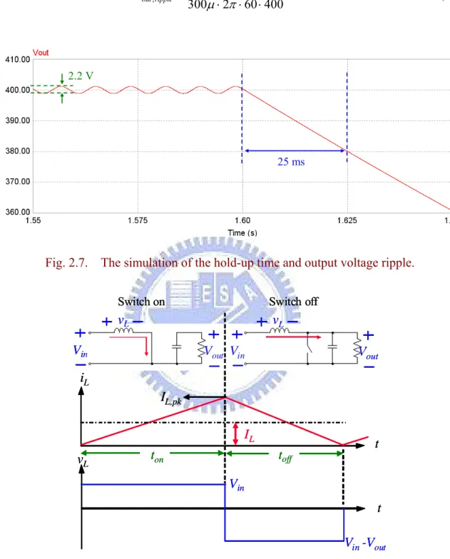
2.6 The simulation of the hold-up time and output voltage ripple. ... 15
2.7 Switching Sequences of the CRM PFC power stage...16
2.8 Typical waveforms of CRM PFC power stage... 18
2.9 The waveform of inductor current... 19
2.10 The switching current waveform... 20
2.11 The diode current waveform ... 21
2.12 The output capacitor current waveform. ... 22
2.13 The power losses on the power components. ... 23
3.1 Overall system block diagram of mixed-signal CRM PFC AC-DC converter .... 25
3.2 Circuits near by the current comparator. ... 27
3.3 The reference waveform of inductor current with hysteresis band. ... 28
3.4 The relationship between hysteresis band and fundamental waveform of line current...28
3.5 Line current waveforms at different hysteresis bands. ... 29
3.6 The relationship between hysteresis band and line current THD... 30
3.7 The relationship between hysteresis band and line current THD with different line voltages. ... 30
3.8 Circuits near by the ZCD comparator. ... 31
3.9 Key switching waveforms of critical mode operation (a) without delay (b) with delay, Td... 32
3.10 The relationship between VZCD,ref and line current THD. ... 32
3.11 Sampling a 120 Hz rectified sinusoidal wave at 480 Hz sampling frequency ...33 3.12 Illustration of the aliasing effect in frequency domain (a) Spectrum of
ix
Spectrum of the sampled signal with ΩS < 2ΩN... 34
3.13 Normalized harmonic ratios for rectified sinusoidal wave... 35
3.14 Quantization effect on rectified input line voltage feedback...36
3.15 The model of quantization effect... 36
3.16 Quantization error introduced by the interface circuits. ... 37
3.17 (a) Square error waveform and (b) harmonic ratio... 38
3.18 (a) Saw tooth error waveform and (b) harmonic components... 39
3.19 Quantization noise from ADC resolution of rectified line voltage feedback. ...40
3.20 The relationship between ADC resolutions and line current THD. ... 41
3.21 Noise introduced by ADC of output voltage feedback. ...41
3.22 Noise introduced by DAC. ... 42
4.1 Mixed-signal control structure of the mixed-signal CRM PFC AC-DC converter. ... 45
4.2 The overall block diagram of the mixed-signal CRM PFC AC-DC converter ... 45
4.3 Average small-signal circuit model of CRM PFC AC-DC converter. ... 47
4.4 Frequency response of transfer function compares with circuit sweeps. ... 48
4.5 The control-to-output transfer function with sample-and-hold. ... 50
4.6 Comparison of the discrete model and continuous model... 51
4.7 The effect of output voltage ripple on inductor current command...52
4.8 The block diagram of digital voltage control loop. ... 54
4.9 Comparing frequency responses of loop gain between circuit sweeps and transfer function...56
4.10 Block diagram of the digital voltage control loop with notch filter. ... 57
4.11 The transient response of output voltage and input line current waveform without notch filter, load changes from 50 % to 100 %. ... 58
4.12 The transient response of output voltage and input line current waveform with notch filter, load changes from 50 % to 100 %. ... 58
4.13 The transient responses of output voltage without load adaptive gain adjustment, load changes from 10 W to 50 W and 60 W to 100 W. ... 60
4.14 The transient responses of output voltage with load adaptive gain adjustment, load changes from 10 W to 50 W and 60 W to 100 W. ... 60
5.1 The experimental board of mixed-signal CRM PFC AC-DC converter. ...61
5.2 The block diagram of L6561. ... 62
5.3 Interrupt configuration in the DSP controller... 63
5.4 The flowchart of voltage loop control. ...64
5.5 The line voltage and output voltage simulation waveforms... 65
5.6 The experimental results of line voltage and output voltage... 66
5.7 The rectified line voltage and inductor current simulation waveforms at 80 W ... 66
5.8 The rectified line voltage and inductor current experimental waveforms at 80 W. ...66
5.9 The line voltage and line current simulation waveforms in 80 W load condition. ... 67
5.10 The experimental results of line voltage and line current waveforms in 80 W load condition. ... 67
5.11 The output voltage and output current simulation waveforms when output load varies from 50 W to 100 W. ... 67
5.12 The experimental results of the output voltage and output current when output load varies from 50 W to 100 W. ... 68
5.13 The experimental results of output voltage and line current waveforms when load varies from 50 W to 100 W and the voltage loop bandwidth is 30 Hz without notch filter. ... 69
5.14 The experimental results of output voltage and line current waveforms when load varies from 50 W to 100 W and the voltage loop bandwidth is 30 Hz with notch filter. ... 69
5.15 Comparing the line current PF without and with notch filter... 70
5.16 Comparing the line current THD without and with notch filter. ... 70
5.17 The experimental results of output voltage transient responses without load adaptive control scheme, load changes from 10 W to 50 W and 60 W to 100 W ...71
5.18 The experimental results of output voltage transient responses with load adaptive control scheme, load changes from 10 W to 50 W and 60 W to 100 W. ...72
Chapter 1
Introduction
1.1
R
ESEARCHB
ACKGROUND ANDR
ECENTD
EVELOPMENTPower supplies for the portable and lighting equipments have become more and more important in daily life. It is well known that power supplies connected to AC line introduced harmonic components to the input line current. The harmonic components cause several problems such as heating, voltage distortion, radiated and conducted noises which will reduce the capability of the mains. And so on, high quality electricity is required and hence the power factor (PF) of electrical application has to be improved. The solutions are referred to power-factor-correction (PFC) techniques which are applied for the front-end of the electric equipments.
The main purposes for the PFC AC-DC converter enforced the input line current to be sinusoidal and in phase with the input line voltage. According to different control topologies, the general approaches, which implement PFC controllers, can be classified into two methods: one is passive approach and the other one is active approach. Traditionally, a full bridge rectifier with passive components is used as AC-DC converter, but the nonlinear line current characteristic will produce significantly harmonic distortions to induce the lower PF. The higher peak value of line current will introduce larger power losses either. In active PFC approaches, PWM converter is employed to overcome the drawback of lower PF in the passive method. The active PFC topologies are composed by energy storage devices, power switch, and the feedback control loop circuit, which enhances the current command changing to follow the variation of output voltage and inductor current.
Recently, active PFC approaches are used in many kinds of fields. According to different operating modes of inductor current, there are continuous-conduction-mode (CCM) PFC and discontinuous-conduction-mode (DCM) PFC. In CCM PFC, the inductor current ripple is usually small enough, so that the line current total-harmonic-distortion (THD) can be reduced as small as possible. In generally, the CCM PFC techniques are widely applied for the applications above 250 W to 10 kW. When the power level is under 250 W, the DCM PFC techniques are widely applied for decreasing the inductor size. Moreover, the control architecture of DCM PFC can be simplified because of the ability of self current following. Among the techniques of DCM PFC, the critical-conduction-mode (CRM) PFC is the most popular solution for low power applications due to the current ripple is only twice of the average current to reduce the cost of the devices in power stages [1]-[4].
There are mainly two traditional approaches, which can be classified by control architectures: the multiplier approach and the voltage-follower approach. The multiplier approach uses a multiplier to generate the shape of the current command. The current operating mode is usually in CCM or in CRM. Although the multiplier has good performance, the control loop is more complicated for design as well. The multiplier accuracy and input range will significantly influence the system performance. There are mainly three current control methods, which are using the multiplier approach: average current control, peak current control, and hysteresis current control [5], [6].
The voltage-follower scheme is simpler than multiplier scheme. Because the current operating mode of voltage-follower method is in DCM or CRM conditions, the components in the power stage have to suffer large variations of voltage and current.
Whatever the multiplier approach or the voltage-follower approach has their own advantages in different applications. Table 1.1 shows the commercial PFC ICs which are generally used.
TABLE 1.1
GENERALLY USED COMMERCIAL PFCICS IN INDUSTRY
IR1150S International Rectifier UC3854, UCC3817 MC33262, MC34262 Texas Instruments FAN4800 FAN7527 Fairchild L4981 L6561, L6562 ST Microelectronics ICE1PCS01 TDA4862, TDA4863 Infineon CCM PFC CRM PFC Manufacturer IR1150S International Rectifier UC3854, UCC3817 MC33262, MC34262 Texas Instruments FAN4800 FAN7527 Fairchild L4981 L6561, L6562 ST Microelectronics ICE1PCS01 TDA4862, TDA4863 Infineon CCM PFC CRM PFC Manufacturer
Although the product life span of telecom equipment will evolve within 18 to 24 months [21], the power supply technology is not developing so quickly. Reusing the previous design could be cost more efficiency. Therefore, developing the products by reusing the power supply product should make flexibility a must. Up until the last couple of years, digital controller has gradually become important for PFC controller due to the communication ability, flexibility, and capability in implementation of nonlinear control. With the advances of the IC industry, it is possible to select a capable and cost effective digital signal processor (DSP). The selection of the DSP may depend more on availability of special on-chip hardware features such as analog-to-digital converters (ADC) and digital-to-analog converters (DAC). The trade-off of PFC controller exists between cost and system performance. Consequently, the issue of cost effectiveness is always the goal of academic research and companies.
1.2
R
ESEARCHM
OTIVATION ANDP
URPOSEIn recent years, the requirements of power supplies grow up quickly. Hence the quality of the power electronic equipments is concerned. Worse power quality will bring many problems such as large harmonics of line current, power pollution, and low efficiency in power transmission. And so on, a large amount of countries have developed relevant laws and regulations for electrical and electric equipment such as EN61000-3-2. These standards can force the equipment products to meet the regulations. Therefore, there are some orientations
to improve the electronic power quality and efficiency.
With the fast evolution of portable commercial electronic equipments, the further requirements of PFC controllers in power system must be more intelligent to adopt the wide range of applications. Therefore, the flexibility of digital controller is noticed.
The analog approach has some deficiencies when compared to the digital control solution: Need to be tuned to each power level. It can not be programmable and hence certainly can not be altered in different applications. Require a relatively large number of extra components (resistors, capacitors etc.). Due to the influence of the thermal effect on power system reduces the life time of analog approach. Analog circuits suffer the disturbance of noise. Therefore, the digital approach is applied for overcoming those drawbacks of analog solutions. The digital approach suffers from the sampling rate and quantization error. The analog approach is more accurate due to avoid the effects of sampling errors, bit resolutions, and computation delays. And so on, combining merits of both analog approach and digital solution is an optimal solution of PFC controllers for electrical techniques [8]-[11].
1.3
T
HER
ESEARCHM
ETHODS ANDS
YSTEMO
VERVIEWThe thesis focuses on the low power consumptive applications, such as portable tools and lighting equipments. The critical conduction mode which is at the boundary of CCM and DCM is more appropriate than DCM PFC in these applications. DCM has higher peak inductor current comparing to CRM in the same average line current. Hence, CRM is generally preferred in low power applications due to the lower maximum current stress in power components, zero-current turn-on, and smaller storage component for example inductance.
The CRM PFC is a variable switching frequency system and its’ maximum value is occurs at the zero crossing of rectified line voltage. If the digital controller is applied for the
current control loop of CRM PFC, it needs extremely large sampling rate to detect the correct peak position of inductor current and then comparing with the current command. The large sampling rate not only introduces significantly power losses but also increases the cost. It stands to reason that the thesis applies analog approach for the current control loop of CRM PFC.
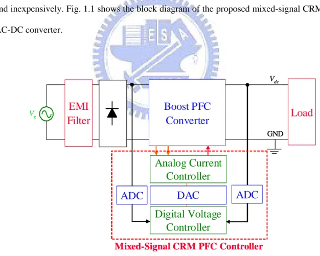
On the other hand, the bandwidth of the voltage control loop has to be low enough to reduce the effect of output voltage ripple. Since the analog approach applies for the inner current loop, the digital solution takes care of the outer voltage loop, which does not require fast clock to implement. The load adaptive gain scheduling can be simply developed by the digital method either. Therefore, the proposed control architecture can be implemented simply and inexpensively. Fig. 1.1 shows the block diagram of the proposed mixed-signal CRM PFC AC-DC converter. Vdc GND Vg
EMI
Filter
Boost PFC
Converter
Digital Voltage
Controller
DAC
Analog Current
Controller
ADC
ADC
Mixed-Signal CRM PFC ControllerLoad
Vdc GND VgEMI
Filter
Boost PFC
Converter
Digital Voltage
Controller
DAC
Analog Current
Controller
ADC
ADC
Mixed-Signal CRM PFC ControllerLoad
1.4
T
HESISO
RGANIZATIONThe thesis is organized as follows:
Chapter 1 introduces the research background, overview the different PFC control topologies, and the motivation of this thesis. The advantages of mixed-signal CRM PFC controller are described.
Chapter 2 gives the different structure and the steady state analysis of the CRM PFC boost converter. The ways to select the storage components and the power consumptions on each component are given.
Chapter 3 focuses on the analysis and design of the sub-circuits, such as current comparator, bit resolutions and sampling rates of ADC, and bit resolutions of DAC, of mixed-signal CRM PFC controller. And so on, the specifications of this mixed-mixed-signal CRM PFC controller can be decided.
Chapter 4 models the control-to-output circuit of mixed-signal CRM PFC by average method. Then the dynamic response is analyzed and the digital voltage controller can be designed by the average small signal model.
Chapter 5 is implemented the mixed-signal CRM PFC by DSP EVM board, TMS320LF2407A, from Texas Instrument (TI) and the analog CRM control IC, L6561, from STMicroelectronics. The experimental results can be shown and analyzed by circuit simulation software (PSIM).
Chapter 2
Analysis of CRM PFC AC-DC Converter
2.1
F
UNDAMENTALP
RINCIPLES OFPF
Improving PF has a lot of advantages such as increasing power usage efficiency, reducing power line capacity, dropping peak line current, and decreasing the power line pollution [7]. Therefore, many nations have formulated some standards for electrical and electronic equipment. In AC network, the power factor (PF) is defined as the ratio of real power to apparent power which can be written as
. Power
Apparent RealPower S
P
PF = = (2-1)
Let vin(t) is sinusoidal line voltage and ig(t) is sinusoidal line current with the line period Tline, the root-mean-square (RMS) values of vg(t) and ig(t) can be defined as follow , ) ( 1 0 2 , = ⋅
∫
s T g s rms g v t dt T V (2-2) . ) ( 1 0 2 , i t dt T I Ts g s rms g = ⋅∫
(2-3) (2-1) can be rewritten as . ) ( ) ( 1 , , 0 rms g rms g T g g s I V dt t i t v T PF s ⋅ ⋅ ⋅ =∫
(2-4) Lower power factor means the power plants have to supply more and more energy tomaintain the same electronic equipment operating. The Fourier series of sinusoidal line current with high order harmonic distortions (ig(t)) can be expressed as
∑
∞ = − ⋅ ⋅ + − ⋅ ⋅ = 2 1 1 1 sin( ) 2 sin( ) 2 ) ( k k k gk g g t I t I t i ω θ ω θ (2-5)where Ig1 is the line current fundamental component, Igk means the kth order component of line current, ω1 is the fundamental frequency, θ1 is the phase angle
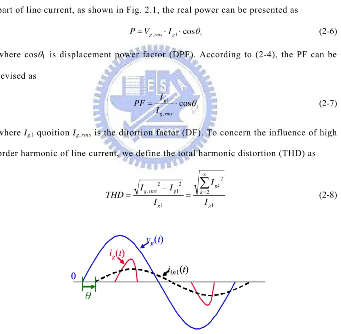
between line voltage and line current fundamental component, and ωk is the kth order frequency. Because the real power is only concerned with the fundamental harmonic part of line current, as shown in Fig. 2.1, the real power can be presented as
1 1 , ⋅ ⋅cosθ
=Vgrms Ig
P (2-6)
where cosθ1 is displacement power factor (DPF). According to (2-4), the PF can be
revised as 1 , 1 ⋅cosθ = rms g g I I PF (2-7)
where Ig1 quoition Ig,rms is the ditortion factor (DF). To concern the influence of high order harmonic of line current, we define the total harmonic distortion (THD) as
1 2 2 1 2 1 2 , g k gk g g rms g I I I I I THD
∑
∞ = = − = (2-8)0
θ
v
g(t)
i
g(t)
i
in1(t)
0
θ
v
g(t)
i
g(t)
i
in1(t)
Then the relationship between THD and DF can be given as 2 ) ( 1 1 DF THD + = (2-9)
and the relationship between PF and THD is
DPF THD PF ⋅ + = 2 ) ( 1 1 (2-10) Consequently, PF can be improved by controlling the line current to shape to line
voltage and hence the high order harmonics of line current can be reduced. Therefore, low THD and high PF are achieved.
2.2
I
NTRODUCTION OFCRM
PFC
C
ONTROLA
RCHITECTURECRM PFC AC-DC converter has the features of zero current turn on and smaller components size, the inductor current peak is the double of line current peak. Therefore CRM PFC is popular for low power applications which are usually under 250 W. Advantages and disadvantages of CRM PFC method are shown in Table 2.1.
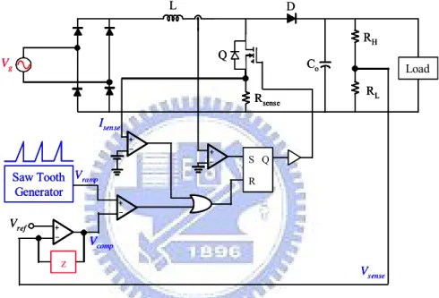
CRM PFC AC-DC converter schemes have two main architectures. One uses a multiplier for generating a current command which is proportional to the rectified line voltage, as shown in Fig. 2.2. The operating principle is shown in Fig 2.3. The switch, Q, is turned off when the sensed switching current achieves the current command, Vmultout, and turned on when the inductor current reaches zero. Due to the control method, the on-time of switch will be a constant value. Then, the line current will trace to the line voltage as shown in (2-11). Therefore, higher power factor and lower harmonic distortion will be ensured. Some commercial CRM control ICs are such as L6561 from STMicroelectronics, TDA4863 from Infineon, MC33262 from ON Semiconductor, UCC28050 from Texas Instruments etc [32].
) ( ) ( , t V t I L t in pk L on = ⋅ (2-11)
TABLE 2.1
ADVANTAGE AND DISADVANTAGES OF THE CRITICAL MODE PFC
Advantage Disadvantage
-Simple Control Scheme:
No need current controller, few external components
-Ease of Stabilization:
No need compensation ramp
-Zero Current Turn On:
Reduce the switching loss
-Current Protection:
Current sensing limits the maximum current
-Variable Switching Frequency:
Grave EMI disturbance
-High Components Tolerance:
The larger current peak value induces more expensive components.
-Zero-Crossing Distortion:
Largest switching frequency and duty
L Load Vg R1 R2 Rsense Co RH RL − + S R Q − + − + z × Vref Multiplier Q Vsense Isense D Vcomp V multout L Load Vg R1 R2 Rsense Co RH RL − + − + S R Q S R Q − + − + − + − + z × Vref Multiplier Q Vsense Isense D Vcomp V multout
Fig. 2.2. The circuit architecture of the CRM PFC with multiplier.
Vin Isense V On Off t Switch Vin Isense V On Off t Switch
The other control strategy has the same purpose to maintain the on-time of switch as a constant value. This architecture is no need of a multiplier but uses the comparing result between the constant ramp, Vramp, which is produced from a saw tooth generator and the output signal of the voltage error amplifier, Vcomp. In this method, rectified line voltage sensing can be eliminated as shown in Fig. 2.4. And the operating principle is shown in Fig. 2.5. These topologies of CRM PFC AC-DC converters are fewer than the topologies with multiplier such as FAN7529 from Fairchild and SG6961 from System General [33].
L D Load Vg Rsense Co RH RL − + − + z Vref Q Vsense Isense − + Saw Tooth Generator − + S R Q Vramp Vcomp L D Load Vg Rsense Co RH RL − + − + z Vref Q Vsense Isense − + Saw Tooth Generator − + S R Q Vramp Vcomp Load Vg Rsense Co RH RL − + − + − + − + z Vref Q Vsense Isense − + − + Saw Tooth Generator − + − + S R Q S R Q Vramp Vcomp
Fig. 2.4. The circuit architecture of the CRM PFC without multiplier.
V
On Offt
V
compV
ramp SwitchV
On Offt
V
compV
ramp SwitchFig. 2.5. Main waveforms of the CRM PFC without multiplier.
This thesis aimed at the CRM PFC AC-DC converter with a multiplier. The analysis and design flow of the control architecture will be given.
2.3
A
RCHITECTURE OFM
IXED-S
IGNALCRM
PFC
AC-DC
C
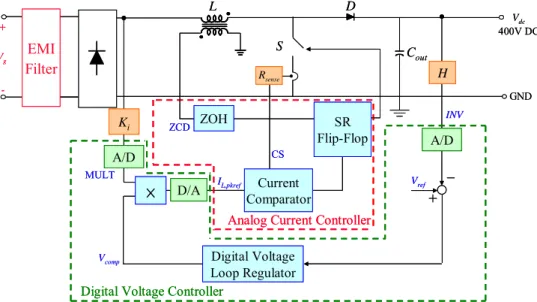
ONVERTERThis section presents a mixed-signal CRM PFC AC-DC converter and the overall system block diagram of the mixed-signal control for the CRM PFC AC-DC converter is as shown in Fig. 2.6. This control architecture includes the inner analog current control loop with the outer digital voltage control loop. The current loop adopts peak current mode control to make inductor current can fast track with command. The voltage loop uses controller to regulate output voltage at setting level and adds the notch filter to eliminate double line frequency, achieve a fast dynamic response, keep the line current with low THD distortion, and maintain high PF. This thesis presents a mixed-signal CRM PFC AC-DC converter which combines the benefits of analog circuit and digital circuit implementation techniques to achieve good dynamic response for output voltage and the low THD with high power factor (PF) for input line current.
Analog PFC control techniques can provide current regulation with low total-harmonic-distortion (THD) on input line current under large input line voltage range which is dominantly adopted for practical implementation. In practice, the feasible control schemes are realized with commercial PFC ICs to meet the requirements both on performance and cost. With the increasingly stringent requirements both on applications and cost issues, digital PFC control techniques are merging to simplify the external control circuits and ease to implement complex control algorithm though circuit design for various applications. However, a pure digital realization of the PFC control scheme requires the realization of accurate and synchronous high frequency signals between the PWM control and feedback sampling. In contrast, mixed-signal realization of the PFC control scheme can combine advantages of fast response analog circuit for current loop control and flexible digital circuit realization for voltage loop control.
Vdc 400V DC GND Vg L D Cout S A/D H + − Vref MULT ZCD CS × Vcomp INV IL,pkref
Digital Voltage Controller
Analog Current Controller
A/D Ki D/A Digital Voltage Loop Regulator EMI Filter + -ZOH sense R Current Comparator SR Flip-Flop Vdc 400V DC GND Vg L D Cout S A/D H + − Vref MULT ZCD CS × Vcomp INV IL,pkref
Digital Voltage Controller
Analog Current Controller
A/D Ki D/A Digital Voltage Loop Regulator EMI Filter + -ZOH sense R Current Comparator SR Flip-Flop
Fig. 2.6. Overall system block diagram of mixed-signal CRM PFC AC-DC converter.
Current Loop Comparator
The current loop comparator compares the sensing voltage across the current sensing resistor below the MOSFET with the inductor current command signal delivered by the multiplier. Then, the current loop comparator can exactly determine the time when the external MOSFET has to be turned off.
The current loop comparator has a hysteresis band to eliminate the noise disturbance from the practical circuits. But this hysteresis band also induces harmonic distortion in the line current. The appropriate value of hysteresis band in the current comparator is an important issue in the design procedure.
Zero Current Detector
The zero current detector (ZCD) function places an important role in CRM PFC AC-DC converter. The comparator of ZCD compares the voltage crossing on the secondary side of the transformer (VZCD) with the zero current detecting reference voltage (Vref,d). When the inductor current is down to zero, the switch will turn on.
resonating with the inductor, an additional delay time (Td) is induced to the inductor current at zero crossing. This delay time will cause the line current harmonic distortion. The zero current detecting reference voltage influences the delay time. Therefore, the proper reference voltage should be determined.
Analog to Digital Converter
Analog-to-digital converter (ADC) is a converter to convert analog signal into digital signal for digital control. The ADC is used at the output voltage feedback sensing and the rectified line voltage sensing.
The signal calculated in digital control system is realized by binary form. The resolution of ADC induces quantization error into the signal. Because the feedback of rectified line voltage determines the shape of inductor current command, the effect of ADC resolution on rectified line voltage is the most significant problem which is induced the harmonic distortion in line current. Moreover, lower sampling rate may introduce aliasing effect. The aliasing effect will also cause the line current high order terms. Therefore, the proper ADC resolution and sampling rate are important.
Digital to Analog Converter
Digital-to-analog converter (DAC) converts the digital current command back to analog signal. The quantization effect will directly influence the shape of inductor current command to induce the high order distortions. Therefore, the DAC resolution should high enough to enforce the line current THD to meet the regulations.
Digital Voltage Control Loop
The voltage compensator eliminates the error part between the feedback output voltage and the reference voltage (Vref). For reducing the effect of output voltage ripple on output of
voltage compensator (Vcomp) the bandwidth of the voltage loop will be set at much lower than the frequency of output voltage ripple.
The analog multiplier has the nonlinear problem and has to implement with complicated circuit. Therefore, the multiplier is implemented in digital approach which only has to concern the quantization effect on digital calculation. The multiplier has two inputs: the first one takes a partition of the instantaneous rectified line voltage and the second one is the output of the voltage compensator. The output of the multiplier (Vmultout) is the inductor current command. Then, this current command will send into the current loop comparator to make the line voltage and line current in phase.
2.4
A
NALYSIS OFCRM
PFC
P
OWERS
TAGEThe main attributes of the components of CRM PFC AC-DC converter, such as output capacitor and inductor value, need to be governed. Then, the power losses on each component should be estimated to calculate the efficiency of the CRM PFC circuit.
2.4.1 Analysis and Design of CRM PFC Power Stage
The design basic specifications are shown in Table 2.2. Then, the main elements of the CRM PFC power stage can be determined.
TABLE 2.2
SPECIFICATIONS OF THE CRMPFCAC-DC CONVETER
Parameter Specification
Rated Output Power (Pout) 100 W
Input Voltage (Vg,rms) 110 Vac
Line Frequency (fline) 60 Hz
Minimum Switching Frequency (fsw) 40 kHz
Output Voltage (Vout) 400 Vdc
Output Voltage Ripple (ΔVout) < 1 %
System Efficiency (η) 90%
The design flows for the main components are as shown in below. There are many factors involved in the design process. However, the equations below are intended to provide a framework for the design.
Determination of Output Capacitor
There are two methods to decide the output capacitor value. One way focuses on the ripple of the output voltage. There are two factors induce the output voltage ripple. One is introduced by the MOSFET switching frequency and the other one is caused by the rectified line voltage which has 120 Hz ripple. The output voltage ripple generated by the MOSFET switching frequency is much smaller than the ripple generated by the rectified line voltage. Assuming the line current is pure sinusoidal. The relationship between average inductor current during a switching period (iL(t)) and input power (Pin) is represented as
) sin( 2 ) ( , t V P t i rms g in L ⋅ ω ⋅ = (2-12)
the input instantaneous power is
(2-13) ). ( sin 2 ) ( 2 t P t Pin = ⋅ in⋅ ω
Therefore, the current flowing through the output capacitor (ic(t)) is . ) ( ) ( dt dV C V P V t P t i out out in out in c =η⋅ −η⋅ = ⋅ (2-14) Substituting (2-13) into (2-14)
[
2⋅sin2( )−1]
. ⋅ ⋅ = ⋅ t C P dt dV V out in out ω η (2-15) Integrated both sides of (2-15) can be given as[
( )]
0.5 sin(2 t) C P V t V V in out out out η ω⎟⋅ ω ⎠ ⎞ ⎜ ⎝ ⎛ ⋅ ⋅ − ⋅ = − ⋅ (2-16)where Vout(t) is equal to [Vout + Δvout,ripple(t)], the combination of output voltage DC term and AC term. The ripple of output voltage is
out in ripple out V C t P t v ⋅ ⋅ ⋅ ⋅ ⋅ − = Δ ω ω η 2 ) 2 sin( ) ( , (2-17)
the peak-to-peak value of output voltage ripple (ΔVout,ripple) can be got . , out in ripple out V C P v ⋅ ⋅ ⋅ = Δ ω η (2-18) According to the output voltage ripple specification from Table 2.2, the output
capacitance can be given as below
μF. 166 400 60 2 % 1 400 100 , = ⋅ ⋅ ⋅ ⋅ = ⋅ ⋅ Δ ⋅ = π ω η out ripple out V v Pin C (2-19)
Another considers the effect of hold-up time. Hold-up time is an important factor related to the amount of energy that the output capacitor needs to store. Generally, hold-up time range from 16 to 50 ms. A great majority of the industry requirement is 20 ms. This takes into consideration the minimum voltage the PFC pre-regulator will allow the output voltage to drop to while sustaining the output load (Usually is down to 95 % of output voltage). The energy storing in output capacitor can be expressed by below energy equation
(
)
. 2 1 2 min , 2 holdup out out out V P t V C⋅ − = ⋅ ⋅ (2-20)According to the specification of hold-up time, the output capacitor can be decided as F. 256 380 400 20 100 2 2 2 2 2 min , 2 μ = − ⋅ ⋅ = − ⋅ ⋅ = m V V t P C out out holdup out (2-21)
Comparing above results of two methods, the output capacitor can be determined by larger one which is 300 μF as shown in Fig. 2.7. The output ripple can be
recalculated V. 2 . 2 400 60 2 300 100 , = ⋅ ⋅ ⋅ = Δ π μ ripple out v (2-22) 2.2 V 25 ms 2.2 V 25 ms
Fig. 2.7. The simulation of the hold-up time and output voltage ripple.
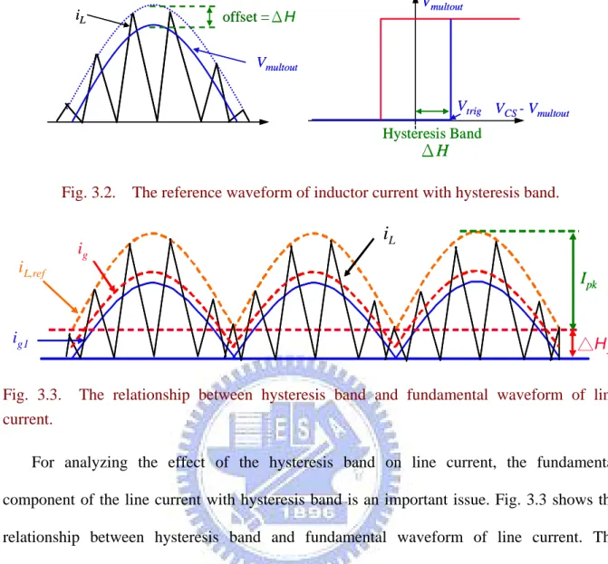
Vout Vout Vin Vin vL vL vL iL Vin Vin -Vout ton toff IL
Switch on Switch off
t t IL,pk Vout Vout Vin Vin vL vL vL iL Vin Vin -Vout ton toff IL
Switch on Switch off
t
t IL,pk
Fig. 2.8. Switching Sequences of the CRM PFC power stage.
Determination of Inductor
The off-time of the MOSFET is based on the input line voltage and the inductance, which also dictates the operating frequency range. The design of the inductor is based on the
switching frequency. As shown in Fig. 2.8, the off-time of the MOSFET is . ) ( ) ( , t V V t I L t in out pk L off = ⋅ − (2-23)
Combining (2-11) and (2-23), the switching frequency (fsw) is
[
]
. ) ( ) ( ) ( 1 , t I V L t V V t V t t f pk L out in out in off on sw ⋅ ⋅ − ⋅ = + = (2-24)The CRM PFC AC-DC converter has variable switching frequency from (2-24). Therefore, the minimum switching frequency will occur at the peak of line voltage.
pk L out pk in out pk in sw I V L V V V f , , , ( ) ⋅ ⋅ − ⋅ ≥ (2-25)
where Vin,pk is the input peak voltage and IL,pk is the peak inductor current. And the average inductor current during a switching period can be represented as
. 2 2 1 , max , , rms g out pk L pk g V P I I ⋅ ⋅ = ⋅ = η (2-26)
According to Table 2.2, the specification of the lowest switching frequency is 40 kHz. Substituting (2-26) into (2-25), the relationship between inductance and the lowest switching frequency is as follow
. 2 2 ) ( min , , 2 , out sw out pk in out pk in P f V V V V L ⋅ ⋅ ⋅ ⋅ − ⋅ ≤ η (2-27)
From (2-27), the inductance should be lower than 835 μF. In this thesis, the inductance is decided as 800 μF. Because that the boost converter operates in the CRM, the relationship between the rectified line voltage and output voltage is
) ( 1 1 t V D Vout ⋅ in − = (2-28)
where D is the duty cycle of the switch. The minimum duty cycle which occurs at the peak of line voltage can be calculated by (2-28).
% 61 400 156 1 1 , min = − = − = out pk in V V D (2-29)
The peak of inductor current (IL,pk) can be expressed as
rms g out rms g pk L V P I I , , , =2⋅ 2⋅ =2⋅ 2⋅ (2-30)
When the line voltage is 110 Vrms, the inductor current peak is 2.57 A. The typical waveforms of the CRM PFC AC-DC converter are shown in Fig. 2.9. At the zero-crossing of line voltage, the energy stored in the inductor is not enough to drive the resonant capacitor to the output voltage. At this critical input line voltage level, the line current distortion will occur.
2.4.2 Calculation of Current RMS Values for Power Components
The efficiency of the CRM PFC power stage is an important issue. Therefore, the RMS current on each component are significant for design procedure [12]-[14].
Rectifier Bridge
The diode of rectified bridge can be approximated by the serial connection of a forward voltage (VF) and a resistance (RF). The current flowing through the rectifier bridge (Iin) is equal to the inductor current (IL). The inductor current waveform is shown in Fig. 2.10. Assuming the switching frequency is much higher than the line frequency. Then, the instantaneous peak value of inductor current is
. sin 2 2 ) ( , , θ = ⋅ ⋅ ⋅ θ rms g in pk L V P i (2-31)
The RMS value of the inductor current triangle over the corresponding switching period Ts (iL,rms(θ)) is represented by . ) sin ( 3 1 ) ( sin sin 1 ) ( 2 , 2 , 2 0 , , θ θ θ θ pk L T t off pk L t on pk L s rms L I dt t Ts t I dt t t I T i s on on ⋅ = ⎥ ⎥ ⎦ ⎤ ⎢ ⎢ ⎣ ⎡ ⎥ ⎥ ⎦ ⎤ ⎢ ⎢ ⎣ ⎡ − ⋅ ⋅ + ⎟⎟ ⎠ ⎞ ⎜⎜ ⎝ ⎛ ⋅ ⋅ ⋅ =
∫
∫
(2-32)T
s toffi
L(t)
i
L,pk(
θ
)
π
0
tonT
s toffi
L(t)
i
L,pk(
θ
)
π
0
tonAs the consequence, the RMS value of the inductor current is
[
]
. 6 1 ) sin ( 3 1 1 ) ( 1 , , 0 2 , 0 2 , , rms in pk L pk L rms L rms L I I I d i I = ⋅ = ⎥⎦ ⎤ ⎢⎣ ⎡ ⋅ ⋅ ⋅ = ⋅ =∫
π∫
π θ π θ θ π (2-33)Then, the power consumption of the four diodes of the rectifier bridge, Ploss,br, can be estimated as follow . 2 4 2 4 2 , , , F rms in rms in F br loss R I I V P ⎥ ⋅ ⎦ ⎤ ⎢ ⎣ ⎡ ⋅ + ⎥ ⎦ ⎤ ⎢ ⎣ ⎡ ⋅ ⋅ ⋅ = π (2-34)
MOSFET and Current Sensing Resistance
CRM PFC AC-DC converter presents a challenge because of the high peak currents which will introduce higher switching conduction losses. The power consumption on the switching current sensing resistance should be concerned either. The waveform of switching current is shown in Fig 2.11. The RMS value of the switching current triangle over the corresponding switching period Ts (iQ,rms(θ)) can be as
. 3 sin sin 1 ) ( , 0 2 , , s on pk L t on pk L s rms Q T t I dt t t I T i on ⎥ = ⋅ ⋅ ⎦ ⎤ ⎢ ⎣ ⎡ ⋅ ⋅ ⋅ =
∫
θ θ θ (2-35)The CRM PFC operates at the border of the CCM and DCM, then the expression gives the duty cycle in a CRM AC-DC converter applications.
T
s toffi
Q(t)
i
L,pk(
θ
)
π
0
tonT
s toffi
Q(t)
i
L,pk(
θ
)
π
0
ton. sin 2 1 ) ( 1 , out rms g out in s on V V V V T t = − θ = − ⋅ ⋅ θ (2-36) As the consequence, the RMS value of the MOSFET current is
[
]
. 3 2 8 1 3 2 sin 2 1 3 ) sin ( 1 ) ( 1 , , 0 , 2 , 0 2 , , out rms g rms g out out rms g pk L rms Q rms Q V V V P d V V I d i I ⋅ ⋅ ⋅ − ⋅ ⋅ = ⎥ ⎥ ⎦ ⎤ ⎢ ⎢ ⎣ ⎡ ⎟ ⎟ ⎠ ⎞ ⎜ ⎜ ⎝ ⎛ ⋅ ⋅ − ⋅ ⋅ ⋅ = ⋅ =∫
∫
π θ θ θ π θ θ π π π (2-37)The conducting switch can be equivalent to a resistance, Rds,on. The power loss on both switch and current sensing resistance, Rsense, is as follow
Ploss,on =
[
Rds,on +Rsense]
⋅IQ,rms2. (2-38)Diode RMS Current
The freewheeling diode of CRM PFC AC-DC converter will be a fast recovery one. The diode current waveform is shown in Fig. 2.12. The RMS value of the diode current over the corresponding switching period Ts, is given by
. 3 sin 2 ) ( sin 1 ) ( , , , s off pk L T t s off pk L s rms D T t I dt t T t I T i s on ⋅ ⋅ = ⎥ ⎥ ⎦ ⎤ ⎢ ⎢ ⎣ ⎡ − ⋅ ⋅ ⋅ =
∫
θ θ θ (2-39)T
st
offi
D(t)
i
L,pk(
θ
)
π
0
t
onT
st
offi
D(t)
i
L,pk(
θ
)
π
0
t
onwhere the ratio of switching off-time over one switching cycle is ( ) 2 , sin . out rms g out in s off V V V t V T t ⋅ ⋅ θ = = (2-40)
As the consequence, the RMS value of the diode current is
[
]
out rms g pk L pk L out rms g rms D rms D V V I d I V V d i I ⋅ ⋅ ⋅ ⋅ = ⎥ ⎦ ⎤ ⎢ ⎣ ⎡ ⋅ ⋅ ⋅ ⋅ = ⋅ =∫
∫
π θ θ π θ θ π π π , , 0 3 2 , , 0 2 , , 2 3 2 sin 3 2 1 ) ( 1 (2-41)and the average current flowing through the diode is equal to the output average current. , . out out avg D V P I = (2-42)
The diode can be also approximated to a serial connection of a forward voltage, VFD, and a resistance, RFD. Therefore, the power consumption can be estimated as
Ploss,diode =VFD⋅ID,avg +RFD⋅ID,rms2. (2-42)
Output Capacitor
The capacitor current is the difference between the diode current and the current absorbed by the load as shown in Fig. 2.13.
iC(t)=iD(t)−iout(t) (2-43)
C
outD
L
R
outi
Di
Ci
outSwitch off
r
CAssuming the output voltage and the output current, iout, will be constant value. out out out out V P I t i ( )= = (2-44)
The RMS value of the capacitor current is
[
]
[
]
. ) ( 2 ) ( ) ( 1 2 2 , 0 2 , 2 0 2 , out rms D out D rms D out out D rms C I I d I i I I d i i I − = ⋅ ⋅ − + = − ⋅ =∫
∫
π π θ θ π θ θ θ π (2-45)The practical capacitor has a serial resistance, rC, which induces power loss on the output capacitor.
Ploss,ESR =IC,rms2⋅rC (2-46)
So that, the total power loss and efficiency of the power stage can be calculated. Power losses on each component are shown in Fig. 2.14.
[
dson sense]
out rms g rms g out on loss R R V V V P P ⋅ + ⎥ ⎥ ⎦ ⎤ ⎢ ⎢ ⎣ ⎡ ⎟ ⎟ ⎠ ⎞ ⎜ ⎜ ⎝ ⎛ ⋅ ⋅ ⋅ − ⋅ ⎟ ⎟ ⎠ ⎞ ⎜ ⎜ ⎝ ⎛ ⋅ = , , 2 , . 3 2 8 1 3 4 π FD out rms g pk L out out FD diode loss R V V I V P V P ⋅ ⋅ ⋅ ⋅ ⋅ + ⋅ = π , 2 , , 2 9 4 F rms in rms in F br loss V I I R P ⎥+ ⋅ ⋅ ⎦ ⎤ ⎢ ⎣ ⎡ ⋅ ⋅ ⋅ = 2 , , , 2 2 4 π C out out rms g pk L ESR loss I r V V I P ⋅ ⎥ ⎥ ⎦ ⎤ ⎢ ⎢ ⎣ ⎡ − ⋅ ⋅ ⋅ ⋅ = 2 , 2 , , 2 9 4 π L D Load Vg Rsense Co Q Vin CRM PFC Controller EMI Filter Iin L D Load Vg Rsense Co Q Vin CRM PFC Controller EMI Filter IinChapter 3
Analysis and Design of Mixed-Signal CRM
PFC AC-DC Converter
3.1
A
NALYSIS ANDD
ESIGN OFA
NALOGC
URRENTC
ONTROLL
OOP3.1.1 Design of the Current Loop Comparator
Switching current is detected by the sensing resistor under the MOSFET, and the sensed voltage compares with the inductor current command from the multiplier output. When the sensed voltage is over the current command, the output of the current comparator will be high. The current comparator output connects to the reset pin of RS flip-flop, causing the MOSFET turned off. The circuits near by the current loop comparator are shown in Fig. 3.1 [15], [16].
RSense PFC IC CS To Gate Driver Vmultout R S Q Current Comparator RS Flip-flop RSense PFC IC CS To Gate Driver R S Q Vmultout Current Comparator RS Flip-flop
Fig. 3.1. Circuit nears by the current loop comparator.
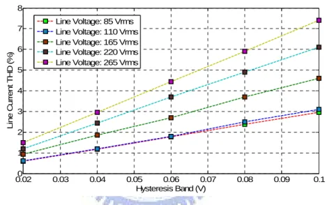
For the current loop comparator of peak current mode control loop, hysteresis band is necessary to eliminate the disturbance of noise to obtain a correct switching signal. Fig. 3.2 shows the reference waveform of inductor current with hysteresis band. However, as mentioned in the previous analysis, over-wide hysteresis band can also induce input current harmonic distortion.
iL Vmultout offset =ΔH iL Vmultout offset =ΔH VCS - Vmultout Vmultout Hysteresis Band ΔH Vtrig VCS - Vmultout Vmultout Hysteresis Band ΔH Vtrig
Fig. 3.2. The reference waveform of inductor current with hysteresis band.
△H1 ig1 iL,ref
i
L Ipk ig ig1 iL,refi
L Ipk igFig. 3.3. The relationship between hysteresis band and fundamental waveform of line current.
For analyzing the effect of the hysteresis band on line current, the fundamental component of the line current with hysteresis band is an important issue. Fig. 3.3 shows the relationship between hysteresis band and fundamental waveform of line current. The hysteresis band is resulting a dc component (ΔH1) in the reference signal of inductor current, iL,ref, ig1 is the input line current fundamental component, and ig is the line current waveform.
In Fig. 3.3, assuming that the switching frequency is much higher than the line frequency, the relationship between the fundamental component of line current and the hysteresis band is as follow rms g out pk pk ref L rms g V P I H d I H d i I , 1 0 1 0 , , 1 4 2 1 2 1 sin ) sin ( 2 2 1 2 1 sin 2 2 1 2 1 ⋅ = ⎟ ⎠ ⎞ ⎜ ⎝ ⎛ ⋅Δ + ⋅ ⋅ = ⋅ ⋅ + Δ ⋅ ⋅ ⋅ = ⋅ ⋅ ⋅ ⋅ =
∫
∫
η π θ θ θ π θ θ π π π (3-1). 1 1 sense R H H =Δ ⋅ Δ (3-2)
If the value of Ipk is given, the line current RMS value can be calculated as
. 4 2 1 2 1 2 1 sin 2 1 1 2 1 1 2 0 1 , ⎟ ⎠ ⎞ ⎜ ⎝ ⎛ ⋅ + ⋅ ⋅Δ +Δ ⋅ = ⎟ ⎠ ⎞ ⎜ ⎝ ⎛ ⋅ ⋅ + ⋅Δ ⋅ =
∫
H H I I d H I I pk pk pk rms g π θ θ π π (3-3)According to (3-3), the THD and PF can be expressed as follow
rms g rms g rms g rms g rms gdis I I I I I THD , 1 2 , 1 2 , , 1 , = − = (3-4) . 1 1 2 , , 1 THD I I PF rms g rms g + = = (3-5)
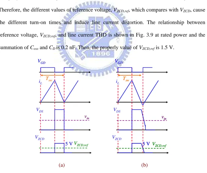
The simulation waveforms of line current with different hysteresis bands are shown in Fig. 3.4. When hysteresis band is 200 mV, the line current will distort at zero crossing. According to (3-1), (3-3), and (3-4), the relationship between hysteresis band influence and THD can be retrieved at the conditions of rated power and 110 Vrms line voltage as shown in Fig. 3.5. Fig. 3.6 shows these relationships with different line voltages. The THD of line current can be determined by harmonic regulation. Therefore, the proper hysteresis band can be selected. In this thesis, the hysteresis band is selected at least under 50 mV to make THD lower than 5 % at rated power. 2.01 2.012 2.014 2.016 2.018 2.02 2.022 2.024 2.026 2.028 2.03 -1 -0.5 0 0.5 1 Time (sec) Li ne C ur re nt ( A ) Hysteresis Band: 0 mV Hysteresis Band: 25 mV Hysteresis Band: 200 mV
0 0.01 0.02 0.03 0.04 0.05 0.06 0.07 0.08 0.09 0.1 0 0.5 1 1.5 2 2.5 3 3.5 Hysteresis Band (V) L in e C urre nt T H D (% ) Purposed Method PSIM Simulation
Fig. 3.5. The relationship between hysteresis band and line current THD.
0.020 0.03 0.04 0.05 0.06 0.07 0.08 0.09 0.1 1 2 3 4 5 6 7 8 Hysteresis Band (V) Li n e C u rre nt T H D (% ) Line Voltage: 85 Vrms Line Voltage: 110 Vrms Line Voltage: 165 Vrms Line Voltage: 220 Vrms Line Voltage: 265 Vrms
Fig. 3.6. The relationship between hysteresis band and line current THD with different line voltages.
3.1.2 Design of ZCD Comparator
Zero-current-detector (ZCD) technique is an important part to maintain that the inductor current operates in the critical mode. It is sensing the voltage of the nodes between the inductor and the power switch, VZCD. When the switch turns on, VZCD is reducing to zero because that the conduction resistor is small and the inductor current linearly increases. When the switch is turns off, VZCD is pulled high to be clamped by the zener diode and the inductor current decays to zero. VZCD compares with a reference voltage, VZCD,ref, and then the ZCD comparator output connects to the S pin of the RS flip-flop, as shown in Fig. 3.7 [17], [18].
PFC IC ZCD To Gate Driver R S Q RS Flip-flop Zero Current Detector VZCD,ref 5 V Coss iL CD PFC IC ZCD To Gate Driver R S Q RS Flip-flop Zero Current Detector VZCD,ref 5 V Coss iL PFC IC ZCD To Gate Driver R S Q RS Flip-flop Zero Current Detector VZCD,ref 5 V Coss iL CD
Fig. 3.7. Circuits near by the ZCD comparator.
The MOSFET turns on with hard switching causing the additional delay, Td, when the circuit operates at CRM. Under this delay region, the voltage of VZCD will not drop to zero straightly as shown in Fig. 3.8 (a) but decade on a constant rate as shown in Fig 3.8 (b). Therefore, the different values of reference voltage, VZCD,ref, which compares with VZCD, cause the different turn-on times and induce line current distortion. The relationship between reference voltage, VZCD,ref, and line current THD is shown in Fig. 3.9 at rated power and the summation of Coss and CD is 0.2 nF. Then, the properly value of VZCD,ref is 1.5 V.
Tsw VGD iL VDS VZCD,ref VZCD 5 V vin Tsw VGD iL VDS VZCD,ref VZCD 5 V vin Tsw VGD iL VDS VZCD,ref VZCD 5 V vin Tsw VGD iL VDS VZCD,ref VZCD 5 V vin Tsw VGD iL VDS VZCD,ref VZCD 5 V vin (a) (b)
Fig. 3.8. Key switching waveforms of critical mode operation (a) without delay (b) with delay, Td.
0.5 1 1.5 2 2.5 3 3.5 4 4.5 2.4 2.6 2.8 3 3.2 3.4 3.6 3.8 4 ZCD Reference Voltage (V) Li ne C u rrent T H D (% )
Fig. 3.9. The relationship between VZCD,ref and line current THD.
3.2
A
NALYSIS ANDD
ESIGN OFD
IGITALV
OLTAGEC
ONTROLL
OOP3.2.1 Issues of Quantization Effect on Digital Control
Implementing digital control on a continuous time system needs an ADC and a DAC for digital and analog signal interface. The striking difference between “analog” and “digital” control is the quality and the amount of information available for the controller to make decisions regarding the operation of the power stage. The control algorithm in digital control system is realized by binary calculation. The presence of a signal of frequency higher than half of the sampling frequency can affect the controller by the aliasing effect [19]-[21].
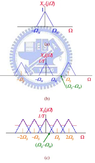
3.2.2 Sampling Frequency
To find a properly sampling rate, the aliasing effect should be concerned. Aliasing is a phenomenon associated with any device or process where the data are divided into individual samples. Any frequency above half of the sampling frequency will cause aliasing effect. Fig. 3.10 shows the aliasing effect by sampling a 120 Hz sinusoidal wave with 150 Hz sampling frequency.