國 立 交 通 大 學
電子工程學系 電子研究所碩士班
碩士論文
非對稱源極/汲極離子佈植及側壁浮閘結構之複
晶矽薄膜電晶體特性
Characterization of Polysilicon Thin Film
Transistors
with Asymmetric Source/Drain Implantation
and with Sidewall Floating Gate structure
研 究 生:林余俊
指導教授:雷添福 博士
非對稱源極/汲極離子佈植及側壁浮閘結構之
複晶矽薄膜電晶體特性
研究生: 林余俊 指導教授:雷添福 博士
國立交通大學
電子工程學系 電子研究所碩士班
摘 要
多晶矽薄膜電晶體近年來受到廣泛開發與研究乃因其與非晶矽薄膜電晶體 比較有高驅動電流,高載子遷移率等特性。然而低溫複晶矽並非完美無暇,其通 道組成的複晶矽結構中含有許多缺陷,而這些結構缺陷會對電晶體的導通電流、 載子遷移率造成劣化的現象。此外,這些缺陷也同時形成了漏電路徑,對元件操 作在關閉狀態時仍有高關閉電流。這阻礙了多晶矽薄膜電晶體在主動式矩陣液晶 顯示器上的應用。過去幾年來已經有許多改善多晶矽薄膜電晶體的漏電現象的論 文被發表,諸如電漿處理、淡摻雜汲極結構和場感應汲極結構等等。然而這些結 構不是需要比傳統製程多的步驟就是需要多一道光罩來達成結構的製備,製程成 本、處理時間和對準錯誤等問題隨著接踵而至。 在本論文中,吾人致力於多晶矽薄膜電晶體的特性研究與新元件結構的開 發。首先,我們提出一個相當簡單的結構,利用傾角的技巧以元件閘極當屏蔽對 元件做不對稱離子佈植。在源極/汲極回火活化後,即自然於一端產生輕摻雜區 域並以此端當汲極,利用輕摻雜區域抑制漏電。在此一新結構中,僅需簡單的製 程流程並且無需多加任一道光罩即可達成。在這個基礎上,我們相信這是一個相當有價值的新元件結構。
另外,我們也提出一個新的元件結構稱之為側壁浮閘結構之複晶矽薄膜電晶 體。利用自我對準的方式在閘極兩端側壁製備浮閘結構,並利用此浮閘受閘極電 廠感應的效果來抑制元件高關閉電流。此外,浮閘再寫入/抹除動作之後並可以 用來記憶載子使元件切換電壓改變。也就是說,此元件具備電子式抹除可寫入唯 讀記憶體(Electrical Erasable Programmable Read Only Memory, PROM)特性。 多晶矽薄膜電晶體的一大優點就是未來可以在主動式液晶面板上製作積體電 路,而記憶體結構則是可以用來儲存影像的單元。此ㄧ側壁浮閘結構具有自我對 準不需多加光罩的優點與以往被提出的多晶矽薄膜電晶體記憶體比較更具微縮 與可用性。
Characterization of Polysilicon Thin Film
Transistors
with Assymetric Source/Drain Implantation and
with Sidewall Floating Gate structure
Student: Yu-Juen Lin Advisor: Dr. Tan-Fu Lei
Departmenet of electronics Engineering & Institute of National
Chiao-Tung University
Abstract
Polycrystalline Silicon Thin-Film Transisitors have been proposed and investigated in recent years since its high driving current and mobility. However, there is some disadvantages in polycrystalline thin-film transistors. One of the most important is the channel region formed by poly grain, and the poly grains have a lot of grain boundary defects. Those defects degrade TFTs’ on-state driving current and mobility. Moreover, grain boundary defects enhance high off-state leakage whenever devices are biased at off-state. The use of conventional polycrystalline thin-film transistors for active matrix liquid crystalline display was hampered by anomalous leakage current. For past decade, many fabrication ways and device structures had been proposed such as plasma treatment, lightly-doped-drain TFTs and field induced drain TFTs. However, these structure need either more process or additional mask than conventional TFTs. And more process or additional mask means higher
fabrication costs and time as well as misalignment.
In this thesis, we have proposed and investigated two new poly-Si TFTs structures. First, we investigate a newstructure named polysilicon thin-film transistors with assymetric source/drain implantation which was fabricated by simply tilt the implant angle. The asymmetric implantation at source/drain forms lightly-doped-drain region beside drain side and it is used to suppress leakage current which results from the high drain side electric field. In this new structure, there is no additional mask needed and the fabrication process is as easy as conventional ones.
Also, we proposed and investigated a new poly-Si TFTs named polysilicon thin-film transistors with sidewall floating gate structure. By self-aligned, two floating gate beside gate electrode are formed. Sidewall floating gate was electrical coupled by the main gate and used to suppress the high off-state current. After program/erase, sidewall polysilicon was able to record electrons such as floating gate in memory cell. In other words, it works as electrical erasable programmable read only memory (EEPROM). One of the important applications to polycrystalline thin-film transistors is used to fabricate system on panel (SOP). Electrical Erasable PROM (EEPROM) devices are very popular for applications such as programmable logic and high density memories. And the realization of LSI circuits and memories for image storage on AMLCD panel was led by polycrystalline silicon TFTs EEPROM’s process. This self-aligned thin-film transistors with sidewall floating gate is higher ability of scale down and applicable.
誌謝
論文的完成,首先要感謝我的指導教授雷添福博士,兩年來的關
心、指導與鼓勵讓我學習作研究的方法與精神。也要謝謝俞正明、謝
明山和郭柏儀學長的熱心協助,使我的實驗得以順利完成。
兩年裡,在工四 309C 與 613 的生活點滴,同窗的照顧,好友的
關懷,無ㄧ不是讓人成長的動力,謝謝李名鎮、張子云、王哲麒、陳
建豪、李宗霖、獻德、小賢等學長的指教,也謝謝松齡、久盟、國誠、
韋翔、任逸、家文、志仰平日的熱心討論和愉快相處,更謝謝國欽、
文俊、宇國、俊彥、榮祥這些日子裡的酸甜苦辣與支持,就像生命是
持續而延長的累積,兩年如果少了各位的任何點滴我也無法肯定自己
是否得以至於此時
。好不容易,這麼一本論文終於完成,多少努力已經忘記,依稀記
得這是父親對兒子的期許,母親向神明祈求的庇蔭,女友無怨接受的
牢騷,二十五年來我只記得做一個有所為的孩子,而卻常常忘記家人
為我朝為青絲暮成雪,無以為報底,謹以這一本論文獻給你們
。Contents
Chinese Abstract English Abstract Acknowledgement Contents Table Captions Figure Captions Chapter 1 Introduction…..……….….…..11.1 Overview of Polycrystalline Silicon Thin-Film Transistor………….……....1
1.2 Motivation……….…..2
1.3 Thesis Outline……….……….4
Chapter 2 Measurements and Device Parameter Extraction………….….…..6
2.1 Measurement……….…….6
2.2 Methods of Device Parameter Extraction………..…….6
2.2.1 Determination of threshold voltage ( Vth )………..6
2.2.2 Determination of subthreshold swing………..7
2.2.3 Determination of field effect mobility (μfe)………7
2.2.4 Determination of on/off current ratio………8
2.2.5 Extraction of grain boundary trap state density (Nt )………9
Chapter 3 Characterization of Polysilicon Thin Film Transistors with Asymmetric Source/Drain Implantation………..12
3.1 Introduction……….12
3.2 Fabrication of Polysilicon Thin Film Transistors with Asymmetric Source/Drain Implantation……….14
3.3 Results and Discussion .……….…...15
3.3.1 Asymmetric Source/Drain Implantation With Source/Drain Exchange Measurement………15
3.3.2 Subthreshold Characteristics………..17
3.3.3 Devices characteristics………....18
3.3.4 Kink Effects……….18
3.3.5 Threshold Voltage roll off………....19
3.4 Hot Carrier Stress……….……….19
3.5 Summary……….…...20
Chapter 4 Characterization of Polysilicon Thin Film Transistors with Sidewall Floating Gate structure……….21
4.1 Introduction………21
4.2 Fabrication of Polysilicon Thin Film Transistors with Sidewall Floating Gate structure.………22
4.3 Results and Discussion………...24
4.3.1 Subthreshold Characteristics……….24
4.3.2 Kink Effects………...…25
4.3.3 Electrical field coupling effect………..…25
4.3.4 Progran and Erase………..…26
4.4 Summary .………..……….………...…...…26
Chapter 5 Conclusions and Feature Works ..………...28
5.1 Conclusions ……….28
5.2 Future Works ………...29
Table Captions
Chapter 3
Table 3.1.1 Split table of asymmetric source/drain implantation TFTs.
Table 3.3.2 Device parameters of asymmetric poly-Si TFTs and conventional TFTs with difference tilt angle.
Figure Captions
Chapter 3
Fig. 3.1.1 The lightly-doped drain polycrystalline TFTs which was proposed by Po-sheng Shih et al. Lightly-doped drain polycrystalline thin film transistors usually need two-step implantation to form the lightly doped region.
Fig. 3.1.2 The offset gate polycrystalline thin-film transistor which was proposed by KEIJI Takana. It needs an additional mask to define the offset region. Misaligned and big series resistance are the main problem. Fig. 3.1.3 The excellent performance of FID structure is believed to due to the
effects of a reduced drain electric field. However, the structure of field-induced-drain TFTs structure needs an additional mask to define the sub-gate and offset region. Also, more thin films must be deposited and the misaligned problem is concerned.
Fig. 3.2.1 The schematic cross sections of the Assymetric Source/Drain Implantation
Fig. 3.2.2 The schematic cross section of conventional device is shown Fig. 3.2.3 The fabrication procedures of these devices
Fig. 3.2.4 A thin oxide was deposited as a buffer of implantation to keep off damages on gate dielectric.
Fig. 3.3.1 The asymmetric source/drain implantation with positive or inversion measurement.
Fig. 3.3.2 The asymmetric source/drain implantation with tilt 30° subthreshold characteristics of inversion measurement.
Fig. 3.3.3 The asymmetric source/drain implantation with tilt 30° ID-VD of inversion measurement.
Fig. 3.3.4 The asymmetric source/drain implantation with tilt 45° subthreshold characteristics of inversion measurement.
Fig. 3.3.5 The asymmetric source/drain implantation with tilt 45° ID-VD of inversion measurement.
Fig. 3.3.6 The ID-VG curves of conventional polycrystalline TFTs and asymmetric source/drain implantation polycryastalline TFTs are shown.
Fig. 3.3.7 The ID-VG curves and Gm of conventional polycrystalline TFTs and asymmetric source/drain implantation polycryastalline TFTs are shown.
Fig. 3.3.8 The ID-VD curves of asymmetric polycrystalline TFTs and conventional TFTs. Asymmetric TFTs shows better kink effect than conventional ones.
Fig. 3.3.9 Threshold voltage roll off of asymmetric source/drain implantation and conventional TFTs. Conventional TFTs show more roll off than asymmetric ones.
Fig. 3.4.1 Threshold voltage variation after hot carrier stress
Fig. 3.4.2 Subthreshold Swing variation after hot carrier stress
Chapter 4
Fig. 4.2.1 The schematic cross section of the conventional TFTs
Fig. 4.2.2 The schematic cross section of polycrystalline silicon with sidewall
floating gate
Fig. 4.2.3 The fabrication procedure of thin-film transistors with sidewall floating gate
Fig. 4.2.4 Poly-Si TFTs with sidewall floating gate Fig. 4.2.5 Poly-Si TFTs with sidewall floating gate
Fig. 4.3.1 SFG TFTs show a better ID-VG curve than conventional TFTs.
Anomalous leakage current is suppressed by the electrical field coupled on floating gate.
Fig. 4.3.2 ID-VD curves of thin-film transistors with sidewall floating gate and
conventional TFTs. Sidewall floating gates TFTs has longer effective channel length than conventional ones.
Fig. 4.3.3 Electric field coupling between gate and drain makes the difference of leakages with different drain voltage.
Fig. 4.3.4 The sketch map of programming and erase measurements
Fig. 4.3.5 Threshold voltage shift after program/erase.The window that threshold voltage shift could reach about 5V.
Chapter 1
Introduction
1.1 Overview of Polycrystalline Silicon Thin-Film Transistor
After the first silicon thin-film transistor demonstration was made in 1966[1], it (TFTs) has attracted much attention. In the past thirty years, poly-Si have been used to a wide range of industrial applications such as thermal printer heads [2], image scanners [3], photo-detector amplifier [4], dynamic access memories (DRAM) [5], static random access memories (SRAM) [6], electrical programming read only memories (EPROM) [7], electrical erasable programming read only memories (EEPROM) [8][9] and active-matrix liquid-crystal display (AMLCD) [10] [11]. Especially the application active-matrix liquid-crystal display (AMLCD) is the major force to promote and advance the development of poly-Si TFT technology.
AMLCDs is one of the most promising candidates for realizing high quality and large area flat panel display. Most flat panel display products now use the a-Si:H TFTs for the pixel switching. However, its low field-effect mobility typically below 1cm2/V‧s. And this make the a-Si:H TFTs prohibited the integration of driver circuitry on the active matrix plate. Another serious problem is that p-channel a-Si:H TFTs usually exhibit very poor performance. After the first demonstration of poly-Si TFT LCD in 1983[10], the interest in poly-Si TFTs has been steadily growing, owing to the features of superior field-effect mobility and better device reliability[12]. High drive capability of poly-Si TFTs enables the integration of driver circuitry on the display panel [13],which further improves system performance and reliability [14],[15], As a result, poly-Si TFTs becomes a solution for realizing high-performance
AMLCD applications.
In recent years, it has been pointed out that the conduction mechanism and performance of poly-Si TFTs were closely related to the existence of poly-Si grains and the properties of grain boundary [16],[17]. As compared with single crystalline silicon, the polycrystalline silicon is rich in grain boundary defects, and the electrical activity of these charge-trapping centers profoundly affects the TFT characteristics. For instance, the defects in channel generate potential barrier which degrade the on-state current of polycrystalline silicon TFTs as well as the various of threshold voltage, field-effect mobility. Additionally, grain boundary defects also create the path of off-state leakage. Leakage current of poly-Si TFTs increases exponentially with difference between gate and drain voltage, and has been attributed to the field emission of carriers via the traps by high electric-field near the drain junction[18]-[20].
Many ways have been proposed to improve the characteristics of poly-Si TFTs. For example, plasma treatment for passivating the defects in channel[21], poly-Si film recrystallized by excimer laser [22]-[29]or metal induced crystallized[30]-[43] to increase the grain size.
Polysilicon TFTs could also be improved by adopting novel device structures. Light doped drain TFTs[44]-[47], offset source/drain[48]-[50], and field-induced drain[51]-[53], dual buffer drain[54], vertical channel[55]-[56] are all among the examples.
1.2 Motivation
Leakage current of polycrystalline TFTs is the most issue of application to AMLCD.It is well known that field emission via grain boundary traps due to high electric field in the drain depletion region would dominate off-state leakage
current[18]. A common method proposed to reduce the severe anomalous leakage current of polycrystalline silicon TFTs is to alleviate the electric field near the drain junction. To achieve this goal, two popular strategies have been proposed, namely, lightly-doped drain (LDD) [37]-[40] and field –induced drain (FID)[44]-[46].
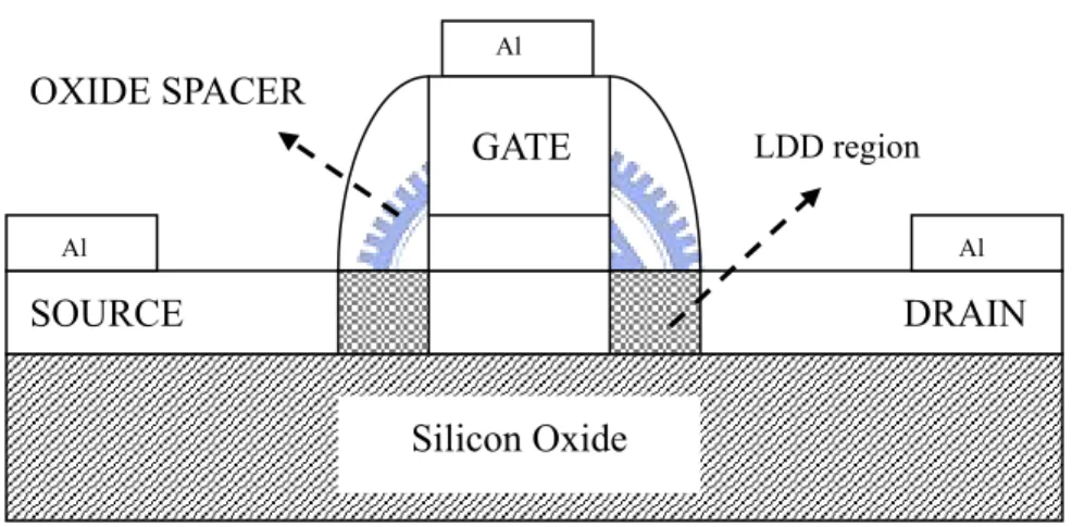
In the LDD structure[38], the source/drain is formed by two step implantation, as shown in Fig. 1.1(a). The LDD implant is to produce a lightly doped section of the source/drain near the channel. LDD region with lower dosage is self-aligned to the gate electrode. It is useful to improve drain leakage by using LDD structure. However, the degradation of on-current due to increase in parasitic resistance introduced in the LDD region is the penalty that must be paid. The required extra lithography and ion doping steps will increase the fabrication costs and make it more complicated in processing.
The second approach, which was originally proposed by Huang et al.[51], employs a field-plate or sub-gate over an undoped offset region in the active channel layer between the drain and the region directly underneath the gate to form a field-induced-drain (FID) region (Fig. 1.1(b)). In this approach, the lightly-doped drain implant that was required in the LDD approach can be skipped. The FID structure has been shown to extremely effective in reducing the off-state leakage, while maintaining good on-state current. The excellent performance of FID structure is believed to due to the effects of a reduced drain electric field. However, the structure of field-induced-drain TFTs structure needs an additional mask to define the sub-gate and offset region. Also, more thin films must be deposited and the misaligned problem is concerned. More films means more fabrication costs. Misalignment means the challenge of uniformity maybe not ignore. In this thesis, we fabricated and investigated two new self-align top gate thin film transistor structures which need no more mask and can shows excellent leakage performance. The first
structure is low temperature thin film transistor with asymmetric source/drain implantation. By the tilt implantation of source/drain method, the offset region in the drain junction form the lightly doped drain. As well as the LDD TFTs structures, the light doped drain region suppresses the field effect near the drain junction. Moreover, by well controlled the lightly doped drain region, this structure can act as a conventional structure in the on-state and turn-on current will not be degraded. The second structure is polycrystalline thin film transistor with sidewall spacer floating gate. In this section we investigated and fabricated a new polycrystalline thin film transistor which shows excellent off-state leakage performance. The floating gate degrade the field-effect in the drain junction by coupling the electric field from gate. Advanced, after program and erase, the subthreshold characteristics shift clearly. It means that this device structure could use for the thin film transistor memories.
1.3 Thesis Outline
This dissertation is organized as follow:
In Chapter 2, the device parameters extraction methods and device measurements will be described.
In Chapter 3, we fabricate and investigate a novel self-aligned poly-Si TFTs with asymmetric source/drain implant. In this chapter we use the process of implantation to materialize the offset region beside the drain junction which form the lightly-doped region after RTA anneal. As well know this lightly-doped-drain junction contributes to restrain the electric field in the drain junction. Also, only one side lightly-doped region after well control would show no degradation at on-state performance. In other words, we contribute a very simple way for polycrystalline silicon thin film transistor without additional mask.
TFTs with sidewall floating gate was realized. This novel structure TFTs also needs no additional mask. It is made by a clever self-aligned procedure. This new TFTs device structure shows not only excellent subthreshold characteristics but also better kink effect. Moreover, the sidewall floating gate acts like the floating gate of flash devices, charges would be stored in it and shift the threshold voltage. So a new TFTs flash was accomplished in our work. However, the program/erase time is not short enough since the tunneling oxide is too thick in this work.
Chapter 2
Measurements and Device Parameters Extraction
2.1 Measurement
In this thesis, we use N&K analyzer to measure the thickness of poly-Si, amorphous-Si, and TEOS oxide films in the fabrication procedure.
HP 4156 semiconductor parameter analyzer with source grounded and body floating performed the current-voltage characteristics of thin film transistor devices.
2.2Methods of Device Parameter Extraction
Many methods have been proposed to extract the characteristic parameters of poly-Si TFT. In this section, the methods of parameter extraction used in this research are described.
2.2.1 Determination of threshold voltage ( Vth )
The threshold voltage Vth is an important MOSFET parameter required for the channel length-width and series resistance measurements. However, Vth is a voltage that is not uniquely defined. Various definitions exist and the reason for this van be found in the ID-VGS curves. One of the most common threshold voltage measurement technique is the linear extrapolation method with the drain current measured as a function of gate voltage at a low drain voltage of typically 50-100 mV to ensure operation in the linear MOSFET region[59]. But the drain current is not zero below threshold and approaches zero only asymptotically. Hence the ID versus VGS curve is extrapolated to ID = 0, and the threshold voltage is determined from the extrapolated or intercept gate voltage VGSi by
2 DS GSi th V V V = − (2.1) Equation ( 2.1 ) is strictly only valid for negligible series resistance. Fortunately
series resistances is usually negligible at the low drain currents where threshold voltage measurements are made. The ID-VGS curve deviates from a straight line at gate voltage below Vth due to subthreshold currents and above Vth due to series resistance and mobility degradation effects. It is common practice to find the point of maximum slope on the ID-VGS curve at that point and extrapolate to ID=0, as illustrated in Fig.2-2.
2.2.2 Determination of subthreshold swing
Sbthreshold swing S.S ( V/decade ) is a typical parameter to describe the control ability of gate toward channel. It is defined as the amount of gate voltage required to increase/decrease drain current by one order of magnitude.
The subthreshold swing should be independent of drain voltage and gate voltage. However, in reality, the subthreshold swing might increase with drain voltage due to short-channel effects such as charge sharing, avalanche multiplication, and punchthrough-like effect. The subthreshold swing is also related to gate voltage due to undesirable factors such as serial resistance and interface state.
In this experiment, the subthreshold swing is defined as one-third of the gate voltage required decreasing the threshold current by three orders of magnitude. The threshold current is specified to be the drain current when the gate voltage is equal to threshold voltage.
2.2.3 Determination of field effect mobility (μfe)
The field-effect mobility (μfe ) is determined from the transconductance ( gm) at low drain voltage. The transfer characteristics of poly-Si TFTs are similar to those of conventional MOSFETs, so the first order I-V relation in the bulk Si MOSFETs can be applied to poly-Si TFTs, which can be expressed as
] 2 1 ) [( G TH D D2 FE D V V V V L W Cox I =µ − − (2-2) where
Cox is the gate oxide capacitance per unit area, W is the channel width,
L is the channel Length, Vth is the threshold voltage.
If VD id much smaller than VG-VTH ( i.e.VD<<VG-VTH ) and VG>VTH, the drain current can be approximated as:
D TH G FE D V V V L W Cox I =µ ( − ) ( 2-3 )
The transconductance is given by
t cons VD G D V I gm = tan ∂ ∂ = ( 2-4) From Eq. ( 2-2 ) and Eq. ( 2-3 ), we find the transconductance to be
D FEV
L WCox
gm= µ ( 2-5 ) Therefore, the field-effect mobility is
Cox WV gm L D FE * = µ ( 2-6 )
2.2.4 Determination of on/off current ratio
On/Off current ratio is one of the most important parameters of poly-Si TFTs since a good performance means not only large On current but also small Off ( leakage ) current. The leakage current mechanism in poly-Si TFTs is not like it in MOSFET. In MOSFET, the channel is composed of single crystalline and the leakage current is due to the tunneling of minority carrier from drain region to accumulation layer located in channel region. However, in poly-Si TFTs, the channel is composed of poly
crystalline. A large amount of trap densities in grain structures attribute a lot of defect states in energy band gap to enhance the tunneling effect. Therefore, the leakage current due to the tunneling effect is much larger in poly-Si TFTs than in single crystalline devices. When the voltage drops between gate voltage and drain voltage increases, the band gap width decreases and the tunneling effect becomes much more severe. Normally we can find this effect in typical poly-Si TFTs ID-VG characteristics where the magnitude of leakage current will reach a minimum and then increase as the gate voltage decreases/increases for n/p-channel TFTs.
There are a lot of ways to specify the On and Off current. In my thesis, take n-channel poly-Si TFTs for examples, the On current and Off current is defined as the when gate voltage equal to 15V and drain voltage is 0.1V ( linear operation mode ). The Off current is specified as the minimum leakage current in linear operation mode for casual cases. V V at plot V I of Current Maximum V V at plot V I of Current Maximum I I DS GS DS DS GS Ds OFF ON 1 . 0 1 . 0 = − = − = (2.7 )
2.2.5 Extraction of grain boundary trap state density (Nt )
The trap state density, which can be determined by the theory established by Levison et al.[60], id based on Seto’s theory[61].
For a thin-film transistor, the source-drain current IDS can be given as following
) 8 exp( ) ( 2 3 GS ox Si c t GS FE DS ox DS V kTC L N q V V C L W I ε µ − = (2.8) Where,
µFE is the field-effect mobility of the carriers. q is the electron charge.
k is Boltzmann’s constant.
εSi is the silicon dielectric constant. T is the temperature.
Nt is the trap-state density. Lc is the channel thickness.
This expression, first developed by Levison et al.[60], is a standard MOSFET’s equation with an activated mobility, which depends on the grain-boundary barrier height as introduced by Step. Levison et al. assumed that the channel thickness was constant and equal to the thickness of the polysilicon film (t). This simplifying assumption is permissible only for very thin film ( t<10 nm ). The trap-state density can be obtained by extracting a straight line on the plot of ln(IDS/VGS) versus 1/VGS at low source-drain voltage and high gate voltages.
Proano et al.[62] thought that a better approximation is to calculate the gate induced carrier channel thickness by solving Poisson’s equation for an undoped material and to define the channel thickness as a thickness which 80 percent of the total charge induced by the gate. Doing so, one obtains
) ( 8 2 fb GS SiO Si ox c V V q kTt L − = ε ε (2.9)
which varies inversely with ( VGS-Vfb). This predicts, by substituting Eq. 2.7 into Eq. 2.6 that ln[IDS/(VGS-Vfb)] versus 1/( VGS-Vfb)2 . We used the gate voltage at which minimum leakage current occurs as Vfb. Effective trap-state density Nt can be determined from the square root of the slope.
Slope q C N ox t = (2.10)
Chapter 3
Characterization of Polysilicon Thin Film Transistors
with Asymmetric Source/Drain Implantation
3.1 Introduction
Polycrystalline thin film transistors technology are promising for AMLCD applications, the anomalous off-state leakage current represent one of important issues [18]. It is well known that field emission via grain boundary traps due to high electric field in the drain depletion region would dominate off-state leakage current[18]. A common method proposed to reduce the severe anomalous leakage current of polycrystalline silicon TFTs is to alleviate the electric field near the drain junction. To achieve this goal, two popular strategies have been proposed, namely, lightly-doped drain (LDD) [37]-[40] and field –induced drain (FID)[44]-[46].
In the LDD structure, the source/drain is formed by two step implantation, as shown in Fig. 3.1.1.[38] The LDD implant is to produce a lightly doped section of the source/drain near the channel. LDD region with lower dosage is self-aligned to the gate electrode. It is useful to improve drain leakage by using LDD structure. However, the degradation of on-current due to increase in parasitic resistance introduced in the LDD region is the penalty that must be paid. The required extra lithography and ion doping steps will increase the fabrication costs and make it more complicated in processing.
The second approach, which was proposed by Keiji Takana et al.[49], employs a undoped offset region besides the gate shown in Fig. 3.1.2. The undoped region can alleviate the drain side electric field effectively. But usually it needs an additional mask to define the offset region. Moreover, the offset region creates a big series
resistance when devices are biased at on state and result in on-state current degradation. This is not what we want for polycrystalline thin film transistors performance.
The third approach, which was originally proposed by Huang et al.[51], employs a field-plate or sub-gate over an undoped offset region in the active channel layer between the drain and the region directly underneath the gate to form a field-induced-drain (FID) region (Fig. 3.1.3). In this approach, the lightly-doped drain implant that was required in the LDD approach can be skipped. The FID structure has been shown to extremely effective in reducing the off-state leakage, while maintaining good on-state current. The excellent performance of FID structure is believed to due to the effects of a reduced drain electric field. However, the structure of field-induced-drain TFTs structure needs an additional mask to define the sub-gate and offset region. Also, more thin films must be deposited and the misaligned problem is concerned. More films means more fabrication costs. Misalignment means the challenge of uniformity maybe not ignore. In this chapter, we fabricated and investigated a new self-align top gate thin film transistor structures which need no more mask and can shows excellent leakage performance. The first structure is polycrystalline thin film transistor with asymmetric source/drain implantation. By the tilt implantation of source/drain method, the offset region beside the drain junction forms the lightly doped drain. As well as the LDD TFTs structures, the light doped drain region suppresses the field effect near the drain junction. Moreover, by well controlled the lightly doped drain region, this structure can act as a conventional structure in the on-state and turn-on current will not be degraded.
3.2 Fabrication of Polysilicon Thin Film Transistors with Asymmetric
Source/Drain Implantation
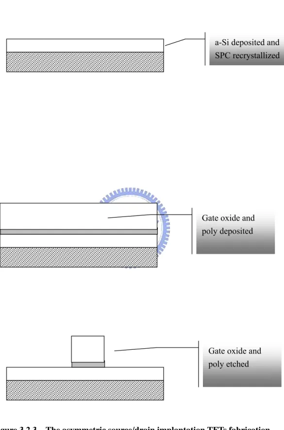
The schematic cross sections of the Assymetric Source/Drain Implantation is shown in Fig. 3.2.1. And the schematic cross section of conventional device is shown in Fig.3.2.2. The fabrication procedures of these devices are described as following (Fig 3.2.3):
Ⅰ. Substrate 100nm p-type single crystalline silicon wafers with (100) orientation were used as the starting materials. After an RCA initial cleaning procedure, 1000 nm thick thermal oxide were grown in steam oxygen ambient at 980°C.
Ⅱ. Poly-Si Thin Film Active Region formation: Undoped amorphous silicon layers of thickness about 50nm or 100nm were deposited by low pressure chemical vapor deposition ( LPCVD ) on buried oxide by pyrolysis of silane ( SiH4) at 550°C. The amorphous silicon films were recrystallized by solid phase crystallization (SPC) method at 600°C for 24hrs in an N2 ambient. These recrystallized poly silicon films were then patterned into active region islands by transformer couple plasma (TCP) etching using the mixture of Cl2 and HBr.
Ⅲ. Gate dielectric and gate electrode formation: In order to decrease the roughness of interface between gate oxide and poly silicon island, thermal oxidation of silicon is excluded. After defining the active region, the wafers were boiled in H2SO4 +H2O2 to ensure cleanliness of the wafers before deposition. A buffered HF dip was performed to remove the native oxide on the silicon surface. The gate insulator was deposited by low pressure chemical vapor deposition (LPCVD) using TEOS and O2 gases at 695°C. After deposition of the gate insulator, a 300nm poly silicon film was deposited immediately on the gate dielectric by LPCVD at 595°C. This poly
silicon was then patterned and etched by transformer couple plasma (TCP) to be the gate electrode. Then remove the gate oxide on source/drain by HF dip.
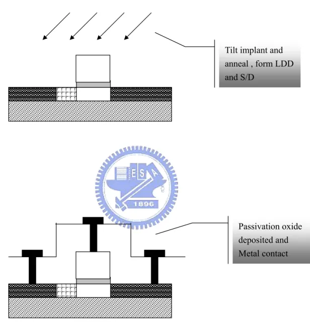
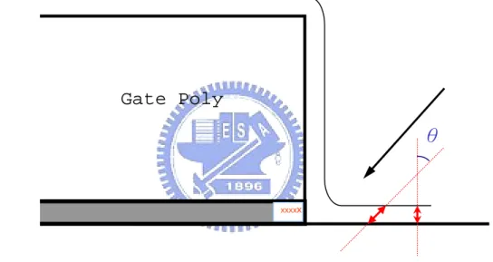
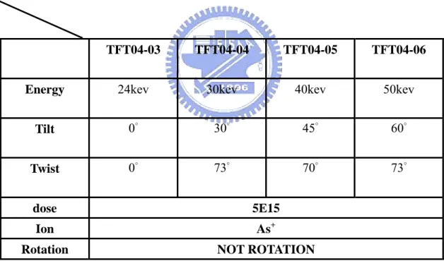
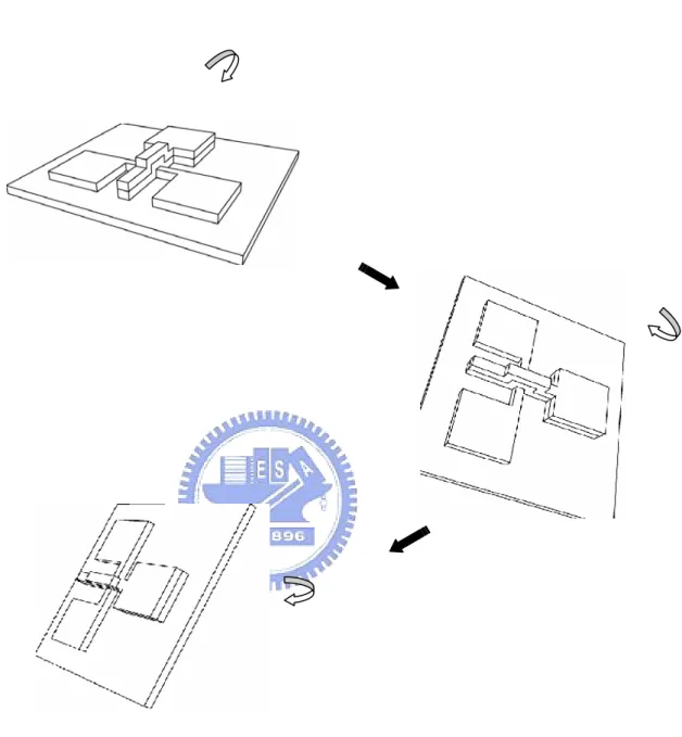
Ⅳ. Source/Drain formation: A thin oxide was deposited as a buffer of implantation to keep off damages on gate dielectric as shown in Fig. 3.2.4 After that source and drain region were implanted by Arsenic (As) as the condition shown in Table 3.1.1. The twist angel come with the tilt angle because the implanter machine roll wafers with three dimensions at the same time as shown in Fig. 3.2.5 The twist angle was fit to the tilt angle by exactly measurement. After ion implantation, the samples were annealed by RTA ambient at 700°C for 20sec and removed the thin oxide by HF dip.
Ⅴ. Passivation oxide and contact metal: Following, 100nm TEOS oxide by LPCVD was deposited and the contact hole was defined. TEOS oxide was etched by buffer oxide etchant (BOE) dip. Then, 900nm Aluminum was sputtered and defined the metal pad. Etching Aluminum and sintering at 400°C in N2 ambient for 30 min.
3.3 Results and Discussion
3.3.1 Asymmetric Source/Drain Implantation With Source/Drain Exchange Measurement
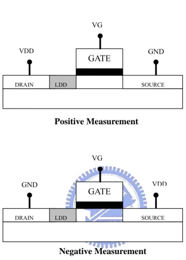
In order to confirm the device structure was fabricated completely, we measure the current-voltage characteristics with exchanging source/drain electrode as shown in Fig. 3.3.1. All devices The with W/L = 10µm/3µm are measured at VDS =0.5 V and 5V.HP 4156 was used to measure all the current-voltage ( I-V ) characteristics and exact device parameters. In this part, results are presented in Fig. 3.3.2 and Fig.3.3.3.
In Fig. 3.3.2, we see subthreshold characteristics of tilt 30° sample get a better performance when the high potential was biased at the drain side. The leakage current of drain side measurement would not be exponentially increasing with gate and drain voltage increased. It means that the lightly-doped-drain region is properly formed only at the drain side and the source side junction is heavily doped. So that the electric field acts at the source side and makes leakage current increasing anomalously when bias was added at the source side. In this figure we are informed that when gate bias at -10 volt, source side leakage current would reach almost 0.1 µA . However, drain side leakage current could be suppressed to 50 pA. There is three order leakage improvement we made. In Fig. 3.3.3, All devices with W/L = 10µm/3µm are measured at VG=5, 6 and 7V. HP 4156 was used to measure. In this figure, the ID-VD curves have been shown. When device is measured at the drain side, better kink effect is performed than measured at the source side. In the tilt 30° samples, when VD was added to 5 V, source side current shows that kink effects is going to happen. However, the drain side measurement was not till the drain voltage increasing to 7 V. That means kink effect happened in polycrystalline TFTs which caused by the high field emission and grain boundary traps is effectively depressed by the lightly-doped-drain ( LDD ). And this lightly-doped-drain exists only at the drain side. In Fig. 3.3.4 and Fig. 3.3.5 we show the sample of tilt 45° asymmetric polycrystalline TFTs. These two figures obviously shows the same characteristics as we described in the before two ones. And we compare Fig. 3.3.4 and Fig. 3.3.5 to Fig. 3.3.2 and Fig. 3.3.3, it shows that the more shift region formed at tilt samples the smaller leakage currents we get and the more shift region formed at tilt samples the better kink effect devices perform. For instance, the leakage current of tilt 45° when VG is -10 V is 2 pA but 50 pA in tilt 30° samples and the kink effect does not happen till VD is 8 V in 45° samples but it happens when VD is 7 V. Also, the size of lighly-doped region affects the
subthreshold characteristics of device.
3.3.2 Subthreshold Characteristics
We compare the device we designed to conventional polycrystalline TFTs . All devices The with W/L = 10µm/3µm are measured at VDS =0.5 V and 5V.HP 4156 was used to measure all the current-voltage ( I-V ) characteristics and extract device parameters. In Fig. 3.3.6 , the transfer curves of conventional polycrystalline TFTs and asymmetric source/drain implantation polycryastalline TFTs are shown. Anomalous leakage current of conventional TFTs increases exponentially with difference between gate and drain voltage caused by the drain side high electric field and grain boundary defects. However the new structure asymmetric source/drain implantation polycrystalline TFTs does not show this shortcoming. This contribution is made by the lightly-doped-drain ( LDD ) junction which suppresses the drain side high electric field when gate bias is strongly negative. Compare this two devices, we see that when gate bias to -10 V the drain leakage of conventional polycrystalline TFTs is about 0.1 µA but asymmetric ones only about 50 pA. There is almost 3.5 order leakage suppressed we made in this experiment. This is a great improvement for polycrystalline TFTs. At the on-state performance, asymmetric polycrystalline TFTs have no difference with conventional ones. Since the lightly-doped region is only at drain side but not at source side. The series resistance of polycrystalline TFTs channel is much bigger than that of metal-oxide-silicon field effect transistors ( MOSFETs ). So the series resistance at on state would not be so serious in polycrystalline thin film transistors. This is why the on-state current not degraded with additional lightly-doped region. As a result, we fabricated a novel new polycrystalline TFTs without any additional mask which show excellent leakage current performance and on-state current performance.
3.3.3 Device characteristics
We extract the device characteristics from the transfer curves in Fig.3.3.7 and show them at Table 3.3.2. First, we survey the on/off ratio of asymmetric and conventional TFTs. Obviously, the on/off ratio of asymmetric polycrystalline TFTs can reach 107 and only 106 at conventional ones. This improvement is made by the leakage current suppressed. The asymmetric source/drain implantation polycrystalline TFTs have lower leakage and the same on-state current than conventional TFTs, so the on off ratio would be improved. The threshold voltage of asymmetric TFTs and conventional TFTs have no difference. Threshold voltage means the voltage gate bias needs to make the channel form inversion layer. This is concerned about the gate oxide thickness, channel quality and etc. There is no difference in our new structure and conventional ones except the source/drain implantation. So the threshold voltage would be the same in these two structures. The inductance Gm and mobility also have the same result. Mobility of polycrystalline TFTs is most affected by channel film quality especially the grain size and grain boundary defects. The bigger grain size channel film has the bigger mobility it owns. The less grain boundary traps it has the better mobility it shows too. The channel film in this experiment are all the same. They are deposited at the same low pressure chemical vapor deposition chamber. This is why they show no difference. At last we check the subthreshold swing. They are also the same in these samples.
3.3.4 Kink Effects
In Fig. 3.3.8, we show the transfer curves of asymmetric TFTs which is tilted 30° and conventional TFTs. All devices with W/L = 10µm/3µm are measured at VG=5, 6 and 7V. HP 4156 was used to measure. In this figure, asymmetric polycrystalline
TFTs show better kink effect performance than conventional TFTs. In the conventional polycrystalline TFTs, when VD was added to 5 V, drain current shows that kink effects is going to happen. However, the drain current of asymmetric source/drain implantation TFTs are not till the drain voltage increasing to 7 V. That means kink effect happened in polycrystalline TFTs which caused by the high field emission and grain boundary traps is effectively depressed by the lightly-doped-drain ( LDD ). Kink effect is an important issue for device operation. Better kink effect means bigger operation range of polycrystalline TFTs and that is what the new structure asymmetric source/drain implantation polycrystalline TFTs do.
3.3.5 Threshold Voltage roll off
In Fig. 3.3.9, devices with different channel length are measured by HP 41 and extracted the threshold voltage of each device. For both conventional and asymmetric source/drain implantation TFTs, threshold voltage is proportional to channel length. However, conventional TFTs threshold voltage roll off is a little serious than asymmetric source/drain implantation. The reason for this phenomenon is the impact ionization in conventional TFTs is more serious than asymmetric TFTs. The impact ionization enhance the threshold voltage roll off.
3.4 Hot Carrier Stress
Hot carrier stress was used to test the long-term reliability of LTPS TFT in this
work. Fig. 3.4.1 illustrates the threshold voltage variations and the degradation in a single TFT under static hot-carrier stress. △Vth is defined as the TFT being kept at a high electric field in the drain junction. Notably, the dc stress conditions are Vds=30V and Vgs=15V for 1000s. This effect occurs due to the higher electric field at the drain
junction. The high electric field promotes impact ionization, resulting in numerous grain-boundary traps being created in the drain junction. The large drain junction electric field during hot carrier stress resulted in sever degradation on conventional structure. On the other hand, the asymmetric TFT exhibited better hot carrier endurance than conventional one due to the drain junction electric field relief. Fig. 3.4.2 and Fig.3.4.3 show subthrehold swing and mobility degradation between asymmetric and conventional structure. Those two factors show the same result as the threshold voltage degradation. In our structure, we can effectively reduce the electric field near the drain side and obtain the optimal results in the hot carrier stress.
3.5 Summary
In this work, we have fabricated and characterized the new structure polycrystalline thin-film transistors featuring top gate. The GILD-like leakage appearing in conventional thin-film transistors could be suppressed obviously in this device and this is contributed by the lightly-doped-drain region which suppresses the drain side electric field. The on/off ratio of asymmetric TFTs could be improved to 107 which is bigger than conventional device about half order. Except the on/off ratio and leakage performance, other parameters such as subthreshold swing, threshold voltage, carrier mobility and etc have no difference with the conventional ones since the fabrication process has no difference with conventional thin-film transistors. It means that this new polycrystalline thin-film transistors match to the process of conventional TFTs. Those process could improve conventional TFTs such as ammonia plasma treatment, hydrogen plasma treatment, laser recrystallized and metal induced recrystallized (MIC)may be used to improve our new design.
Chapter 4
Characterization of Polysilicon Thin Film Transistors
with Sidewall Floating Gate Structure
4.1
Introduction
Anomalous leakage current of polycrystalline silicon TFTs is an important issue for industrial application. In recent years, it has been pointed out that the conduction mechanism and performance of poly-Si TFTs were closely related to the existence of poly-Si grains and the properties of grain boundary[18]. As compared with single crystalline silicon, the polycrystalline silicon is rich in grain boundary defects, and the electrical activity of these charge-trapping centers profoundly affects the TFT characteristics. For instance, the defects in channel generate potential barrier which degrade the on-state current of polycrystalline silicon TFTs as well as the various of threshold voltage, field-effect mobility. Additionally, grain boundary defects also create the path of off-state leakage. Leakage current of poly-Si TFTs increases exponentially with difference between gate and drain voltage, and has been attributed to the field emission of carriers via the traps by high electric-field near the drain junction[18]-[20]. Recently, many ways have been proposed to suppress the anomalous leakage current such as plasma passivation, recrystallized by laser and device structure improvement. In this section, we fabricate and propose an new structure which shows better device performance and has memory characteristics.
Polycrystalline silicon thin-film transistors have been widely used to integrate driver circuits for AMLCD’s [63].The degree of circuit integration will continue to increase as device characteristics improve further, so that entire systems may be
integrated on a glass substrate soon. The entire system will include memories, such as SRAM and EEPROM.Electrical Erasable PROM (EEPROM) devices are very popular for applications such as programmable logic and high density memories. One of the important applications to polycrystalline thin-film transistors is used to fabricate system on panel (SOP). In this chapter, we design and fabricate a simple self-aligned sidewall floating gate polycrystalline TFTs. This new structure of polycrystalline TFTs shows not only program/erase characteristics but also better on/off ratio and smaller leakage. The structure also shows less fabrication cost and elabrateness than others [64]-[66]. In the following sections, we will describe distinctly the fabrication process and device characteristics.
4.2
Fabrication of Polysilicon Thin Film Transistors with Floating Gate
structure
The schematic cross section of the conventional TFTs is shown in Fig. 4.2.1. And the schematic cross section of polycrystalline silicon with sidewall floating gate is shown in Fig.4.2.2. The fabrication procedures of these devices are described as following:
Ⅰ. Substrate 100nm p-type single crystalline silicon wafers with (100) orientation were used as the starting materials. After an RCA initial cleaning procedure, 1000 nm thick thermal oxide were grown in steam oxygen ambient at 980°C.
Ⅱ. Poly-Si Thin Film Active Region formation: Undoped amorphous silicon layers of thickness about 50nm or 100nm were deposited by low pressure chemical vapor deposition ( LPCVD ) on buried oxide by pyrolysis of silane ( SiH4) at 550°C. The amorphous silicon films were recrystallized by solid phase crystallization (SPC)
method at 600°C for 24hrs in an N2 ambient. These recrystallized poly silicon films were then patterned into active region islands by transformer couple plasma (TCP) etching using the mixture of Cl2 and HBr.
Ⅲ. Gate dielectric and gate electrode formation: In order to decrease the roughness of interface between gate oxide and poly silicon island, thermal oxidation of silicon is excluded. After defining the active region, the wafers were boiled in H2SO4 +H2O2 to ensure cleanliness of the wafers before deposition. A buffered HF dip was performed to remove the native oxide on the silicon surface. The gate insulator was deposited by low pressure chemical vapor deposition (LPCVD) using TEOS and O2 gases at 695°C. After deposition of the gate insulator, a 300nm poly silicon film was deposited immediately on the gate dielectric by LPCVD at 595°C. This poly silicon was then patterned and etched by transformer couple plasma (TCP) to be the gate electrode. After removing the gate oxide on source/drain by HF dip.
Ⅳ. After RCA clean,50 nm TEOS oxide and 250nm poly silicon were deposited on the samples. Following, 300nm thick TEOS oxide was deposited and etched to form the oxide spacer which would be the hard mask of sidewall floating gate.
Ⅴ. Etching the oxide spacer by RIE and the etch the poly silicon by transformer chemical plasma (TCP). It is important to notice that when etching poly the over etching should be much longer than usual since the active region of TFTs rating from the buffer oxide. Then removing the gate oxide on source/drain by HF dip.
Ⅳ. Source/Drain formation: Source and drain region were implanted by Phosphorus (P) at 18 kev to a dose of 5E15 cm-2 .
Ⅴ. Passivation oxide and contact metal: Following, 100nm TEOS oxide by LPCVD was deposited and the contact hole was defined. TEOS oxide was etched by buffer oxide etchant (BOE) dip. Then, 500nm Aluminum sputtering and define the metal pad. Etching Aluminum and sintering at 400°C in N2 ambient for 30 min. The fabrication procedure has been shown in Fig.4.2.3 and the SEM figures are shown in Fig, 4.2.4.
4.3 Results and Discussion
4.3.1 Subthreshold Characteristics
We compare the polycrystalline tin-film transistors with sidewall floating gate to conventional polycrystalline TFTs . All devices The with W/L = 10µm/3µm are measured at VDS =0.5 V and 5V.HP 4156 was used to measure all the current-voltage ( I-V ) characteristics and extract device parameters. In Fig. 4.3.1 , the ID-VG curves of conventional polycrystalline TFTs and polycrystalline thin-film transistors with sidewall floating gate are shown. Anomalous leakage current of conventional TFTs increases exponentially with difference between gate and drain voltage caused by the drain side high electric field and grain boundary defects. However the new structure polycrystalline thin-film transistors with sidewall floating gate does not show this shortcoming. This contribution is made by the floating gate which was electrical field coupled by the main gate. Compare this two devices, we see that when gate bias to -10 V the drain leakage of conventional polycrystalline TFTs is about 0.1 µA but thin-film transistors with sidewall floating gate only about 0.01 µA. There is almost 2 order leakage suppressed we made in this experiment. This is a great improvement for polycrystalline TFTs. At the on-state performance, polycrystalline thin-film
transistors with sidewall floating gate have better on current than conventional ones. Since the sidewall floating gate is coupled with positive charge when gate and drain are both bias at positive voltage. As a result, we fabricated a novel new polycrystalline TFTs without any additional mask which show excellent leakage current performance and better on-state current performance.
4.3.2 Kink Effects
In Fig. 4.3.2, we show the ID-VD curves of thin-film transistors with sidewall floating gate and conventional TFTs. All devices with W/L = 10µm/3µm are measured at VG=5, 6 and 7 v. HP 4156 was used to measure. In this figure, polycrystalline thin-film transistors with sidewall floating gate shows better kink effect performance than conventional TFTs. In the conventional polycrystalline TFTs, when VD was added to 5V, drain current shows that kink effects is going to happen. However, the drain current of thin-film transistors with sidewall floating gate are not till the drain voltage increasing to 6.5V. That means kink effect happened in polycrystalline TFTs which is caused by the high field emission and grain boundary traps is smaller in the new structure we designed. There are two reasons for this phenomenon. One is that two sidewall floating gates about 0.6µm add the effective channel length so the electric field which is inverse proportion to channel length ( d ) is smaller than in conventional ones. The other is the maximum electric field peak not under the edge of gate. So that kink effect is better for the sidewall floating gate than conventional TFTs.
4.3.3 Electrical field coupling effect
We measure the ID-VG with different drain voltage to check the variation of leakage. When drain is biased at small voltage such as 1V, leakage current shows well
degradation by the subgate because gate couples the floating gate more than drain. When drain is biased at big voltage such as 9V and 11V, leakage current shows no degradation since gate coupling effect on floating gate is equal to drain coupling effect. Those are shown at Fig. 4.3.3.
4.3.4 Progran and Erase
In Fig. 4.3.4 , programming and erase measurements are shown. During programming, a negative high voltage is applied to the main gate for ten seconds, and electrons tunnel into the sidewall floating gate from main gate. The negative charges in floating gate shift the threshold voltage ( Vth ) to a high value. During erase, a positive high voltage is applied to the main gate for ten seconds, and electrons tunnel into the main gate from sidewall floating gate. The positive charges in floating gate shift the threshold voltage ( Vth ) to a low value. The threshold voltage shift has been shown in Fig. 4.3.5. The window that threshold voltage shift could reach about 5V. The programming and erase time is as long as ten seconds, it seems a little long than usually memory cell. This is caused by the thick tunneling oxide. Tunneling oxide in usual memory cell is under 3 nm but 50nm in our work.
4.4 Summary
In this section, a polycrystalline thin-film transistors with sidewall floating gate has been fabricated and demonstrated. This new structure is self-aligned and needs no additional mask. By coupling the electric field on the floating gate, the device shows better subthreshold characteristics and kink effect than conventional TFTs. The on/off ratio and anomalous leakage current have been improved.
shows threshold voltage shift after program/erase. It means this device could be used to electric erasable programmable read only memory (EEPROM). And the realization of LSI circuits and memories for image storage on AMLCD panel was led by polycrystalline silicon TFTs EEPROM’s process.
Chapter 5
Conclusions and Future Works
5.1 Conclusions
In this thesis, two novel polycrystalline thin-film transistors were proposed and fabricated.
In Chapter 3, the polycrystalline thin-film transistors with asymmetric source/drain implantation has been fabricated. This new structure without any additional mask added and the fabrication process is the same with conventional TFTs. The only difference between asymmetric and conventional TFTs is the tilt angle which bring with the twist angle. The height of gate and the twist angle decide the offset region of the dopant in drain side. After diffusion this region becomes light-doped region. By well controlled the lightly doped drain region, this structure can act as a conventional structure in the on-state and turn-on current will not be degraded. As a result, the anomalous leakage current of thin-film transistors has been suppressed by the lightly doped drain junction and the on-state current shows no degradation. A new structure thin-film transistor with high on/off ratio and excellent off-state performance has been obtained.
In Chapter 4, the polycrystalline thin-film transistors with sidewall floating gate has been fabricated. The first purpose of the sidewall floating gate is suppressing the electric field in drain side and suppresses the anomalous drain leakage in off-state bias. In the ID-VG curves and ID-VD curves, the smaller leakage and better kink effect have been shown. The other purpose of the sidewall poly is used as the floating gate in memories to storage electron. After programming and erase, devices show threshold voltage and the shift window is about 5V. It means that a successful electrical erasable
programmable read only memory was fabricated.
5.2 Future Works
Although these two new structure thin-film transistors has been proposed and fabricated, however it needs more investigation. For asymmetric source/drain implantation, the shift region for tilt implant and diffusion in polycrystalline film could be more modified. For floating gate structure, the tunneling oxide could be decreased to reduce the program/erase time. And both of these devices have never been plasma treatment. They could also fabricated by other recrystallized ways such as excimer laser crystallized (ELC) or metal induced crystallized (MIC) to enhance their mobility, subthreshold swing and etc.
References
[1] C. H. Fa and T. T. Jew, “The poly-Silicon insulated-gate field-effect transistor,” IEEE Trans. Electron Devices, vol. 13, no. 2, p290,1966
[2] Y. hayashi, H. Hayashi, M. Negishi, T. Matsushita, “A Thermal Printer Head woth CMOS Thin-Film Transistors and Heating Elements Integrated on a Chip,” IEEE Int. Solid-State Circuits Conference, p.266, 1988.
[3] T. Kaneko, Y. Hosohawa, M. Tadauchi, Y. Kita, and H. Andoh, “400 dpi Integrated Contact Type Linear Image woth Poly-Si TFT’s Analog Readout Circuits and Dynamic Shift Registers,” IEEE Trans. Electron Devices, vol. 38, no. 5, pp.1086-1093,1991
[4] M. G. Clark, “Current Status and Feature Prospects of Poly-Si,” IEE proc. Circuits Devices Syst., vol. 141, no. 1, p.3, 1994
[5] S. D. S. Mahli, H. Shichijo, S. K. Banerjee, R. Sundaresan, M. Elahy, G. P. Pillack, W. F. Richardson, A. H. Shah, L. R. Hite, R. H. Womack, P. K. Chatterjee, and H. W. Lam, “Characteristics and Three-Dimensional Integration o MOSFET’s in Small-Grain LPCVD Polycrystalline Silicon,” IEEE Trans. Electron Devices, vol. 32, p. 258, 1985
[6] S. Batra, “Development of Drain-Offset (DO) TFT Technology for High Density SRAM’s,” Ectended Abstracts, vol.94-2, in Electrochemical Soc. Fall Mtg., Miami Beach, FL, Oct. p.677,1994
[7] K. Yoshizaki, H. Takahashi, Y. Kamigaki, T. Yasui, K. Komori, and H. Katto, ISSCC Digest of Tech. Papers, p.166, February 1985
[8] M. Cao, et al., “A Simple EEPROM Cell using Twin Polysilicon Thin-Film Transistors,” IEEE Electron Device Lett., vol.15, p.304,1994
[9] N. D. Young, G. Harkin, R. M. Bunn, D. J. McCulloch, and I. D. French, “The Fabrication and Characterization of EEPROM Arrays on Glass Using a Low Temperature Poly-Si TFT Process,” IEEE Trans. Electron Devices, vol. 43, no. 11, pp1930-1936, 1995
[10] S. Morozumi, K. Oguchi, S. Yazawa, T. Kodaira, H. Ohshima, and T. Mano, “B/W and color LC video display addressed by poly-Si Thin-Film Transistors,” IEEE Photonic Tech. Lett., vol. 5, p.319, 1993
[11] R. E. Proano, R. S. Misage, D. Jones, and D. G. Ast, “Guest-Host Active Matrix Liquid-Crystal Display using High –Voltage Polysilicon Thin-Film Transistors,” IEEE Trans. Electron Devices, vol. 38, p.1781,1991
[12] J. R. Ayres and N.D. Young, “Hot carrier effects in devices and circuits formed from poly-Si,” IEE proc. Circuits Devices Syst., vol.141, no.1, pp.34-38, 1994 [13] S.D. Brotherton, N.D. Young, M. J. Edwards, A. Gill, M. J. Trainor, J. R. Ayres, I.
R. Clarence, R. M. Bunn, and J. P. Gowers, “Low temperature furnace processed poly-Si TFT AMLCDs,” in IDRC Digest, Santa Ana, CA: SID, pp.130-131, 1994 [14] I. W. Wu, “Low temperature poly-Si TFT Technology for AMLCD application,”
Tech. Dig. Active Matrix Liquid Crystal Display, p.7, 1995
[15] T. Serikawa, S. Shirai, A. Okamoto, and S. Suyama, “Low temperature
fabrication of high mobility poly-Si TFT’s for large-area LCD’s,” IEEE Trans. Electron Devices, vol.36 , p.1929,1989
[16] J. Y. W. Seto, “The electrical properties of polycrystalline silicon films,” J. Appl. Phys., vol.46, no.12, p.5247-5254,1975
[17] G Baccarani, B. Ricco and G. Spadin, “Transport properties of polycrystalline silicon films,” J. Appl. Phys., vol.49, p.5565, 1978
[18] J. G. Fossum, A. Ortiz-Code, H. Shicjijo, and S. K. Banerjee, “Anomalous Leakage Current in LPCVE Ploysilicon MOSFET’s,” IEEE Trans. Electron
Devices, vol.32 , pp.1878-1884,1985
[19] I. W. Wu, A.an G. Lewis, Tiao-Yuan Huang, Warren B. Jackson, and Anne Chiang, “Mechanism and Divice-to-Device Variation of Leakage Current in Polysilicon Thin-Film Transistor,” in IEDM Tech. Dig. ,pp.867-870, 1990 [20] K. R. Olasupo, M. K. Hatalis, “Leakage Current Mechanism in Submicron
Polysilicon Thin-Film Transistors,” IEEE Trans. Electron Devices, vol. 43, p.1218-1223,1996
[21] Fang-Shing Wang; Meng-Jin Tsai; Huang-Chung Cheng; “The effects of NH plasma passivation on polysilicon thin-film transistors
3
” Electron Device Letters,
IEEE , Volume: 16 , pp.503 - 505, Nov. 1995
[22] T. Sameshima, S. Usui and M. Sekiya, “XeCl excimer laser annealing used in the fabrication of poly-Si TFTs,” Electronchem. Solid-State Lett., vol.
7no.5,pp.276-278,1986
[23] D. H. Choi, E. Sadayuki, O. Sugiura and M. Matsumra, “Excimer-laser
crystallized poly-Si TFT’s with mobility of more than 600 cm2/V-s,” IEEE Trans. Electron Devices, vol. 41, no. 11, p.2129, 1993
[24] K. Shimizu, O. Sugiura and M. matsumra, “High-mobility poly-Si thin-film transistors fabricated by a novel excimer laser crystallization method,” IEEE Trans. Electron Devices, vol. 40, no. 1, pp.112-117, 1993
[25] Y. F. Tang, S. R. P. Silva, and M, J, Rose, “Super sequential lateral groeth od Nd:YAG laser crystallized hydrogenated amorphous silicon,” Appl. Phys. Lett., vol.78 , pp.186-188, 2001
[26] Y Helen, R. Dassow, M. Nerding, K. Mourgues, F. Raoult, J. R. Kohler, T.
Mohammed-Brahim, R. Rogel, O. Bonnaud, J. H. Wermer, and H. P. Strunk, “High mobility thin film transistors by Nd: YVO4-laser crystallization,” Thin
Solid Films, vol.383, pp.143-146, 2001
[27] T. Morita and T. Noguchi, “UV pulsed laser annealing of Si+ implanted silicon filn and low-temperature super thin film transistors,” Jap. J. Appl. Phys., vol.28, p.L309,1989
[28] Akito Hara, Fumiyo Takeuchi, Michiko Takei, Katsuyuki Suga, Kenichi Yishino, Mistsuru Chida, Yasuyuki Sano, and Nobuo Sasaki, “High-prtfotmance polycrystalline silicon thin film transistors on non-1lkali glass produced using continuous wave laser lateral crystallization,” Jap. J. Appl. Phys., part 2, vol.41, pp.L311-L313,2002
[29] Bohuslav Rezek, Chistoph E. Nebel, and Martin Stutzmann, “polycrystalline silicon thin films produced by interference laser crystallization of amorphous silicon,” Jap. J. Appl. Phys., part 2, vol.38, pp.L1083-L1084,1999
[30] G. Radnoczi, A. Robertsson, H. T. G. Hentzell, S. F. Gong, and M. A. Hasan, “Al induced crystallization of a-Si,”J. Appl. Phys., vol.69, pp.6394-6399,1991
[31] S. W. Russell, Jian Li, and J. W. Mayer, “ In situ observation of fractal growth during a-Si crystallization in a Cu3Si matrix,” J. Appl. Phys., vol.70, pp.5153-5155,1991
[32] Soon young Yoon, Ki Hyung, Chae Ok Kim, Jae Young Oh, and Jin Jang, “Low temperature metal induced crystallization of amorphous silicon using a Ni solution,” J. Appl. Phys., vol.82 , pp.5865-5867,1997
[33] Bo Bian, jian Yie, Voquan Li, and Ziqin Wu, “Fractal formation in a-Si:H/Ag/a-Si:H films after annealing,” J. Appl. Phys., vol.73 , pp.7402-7406,1993
[34] L. Hultman, A. Robertsson, H. U. G. Hentzell, I. Engstrom, and P. A. Psaras, “Crystallization of amorphous silicon during thin-film gold reation,” J. Appl. Phys., vol.73 , pp.3647-3655,1987
[35] Zhonghe Jin, Gurutaj A. Bhat, Milton Yeung, Hoi S. Kwok, and Man Wong, “nickel induced crystallization of amorphous silicon thin films,” J. Appl. Phys., vol.84 ,pp.194-200,1998
[36] Yunosuke Kawazu, Hiroshi Kudo, Seinosuke Onari, and Toshihiro Arai, “Low-temperature crystallization of hydrogenated amorphous silicon induced by nickel silicide formation,” Jap. J. Appl. Phys., part 1, vol.29, pp.2698-2704, 1990
[37] Seko-Woon Lee, Yoo-Chan Jeon, and Seung-Ki Joo, “Pd induced lateral crystallization of amorphous Si thin films,” Appl. Phys. Lett., vol.66 , pp.1671-1673,1995
[38] Seok-Woon Lee and Seung-Ki Joo, “Low temperature poly-Si thin-film transistor fabrication by metal-induced lateral crystallization,” IEEE Electron Device Lett., vol.17, pp.160-162,1996
[39] Seok-Woon Lee, Tae-Hyung Ihn, and Seung-Ki Joo, “Fabrication of high-mobility p-channel poly-Si thin film transistors by self-aligned metal-induced lateral crystallization,” IEEE Electron Device Lett., vol.17, pp.407-409,1996 [40] Zhonghe Jin, Gurutaj A. Vhat, Milton Yeung, Hoi S. Kwok, and Man Wong,
“nickel induced crystallization of amorphous silicon thin films,” IEEE Trans. Electron Devices, vol. 46, no. 1, pp.78-82, 1999
[41] Hansuk Kim, J. Greg Couillard, and Dieter G. Ast, “Kinetic of silicide-induced crystallization of polycrystalline thin-film transistors fabricated from amorphous chemical-capro deposition silicon,” Appl. Phys. Lett., vol.72 , no.12,
pp.803-805,1998
[42] Zhonghe Jin, Hoi S. Kwik, and Man Wong, “Performance of thin-film transistors with ultrathin Ni-MILC polycrystalline silicon channel layers,” IEEE Trans. Electron Device, vol.20, pp.167-169,1999
[43] Zhiguo Meng, Mingxiang Wang, and Man Wong, “High performance low temperature metal-induced unilaterally crystallized polycrystalline silicon thin film transistors for system-on-pamel application,” IEEE Trans. Electron Devices, vol.47 , pp.404-409, 2000
[44] Kwon-Young Choi; Min-Koo Han; “A novel gate-overlapped LDD poly-Si thin-film transistor” Electron Device Letters, IEEE , Vol. 17 , pp.566 – 568, Dec. 1996
[45] Byung-Hyuk Min; Kanicki, J.; “Electrical characteristics of new LDD poly-Si TFT structure tolerant to process misalignment” Electron Device Letters, IEEE , Vol. 20 , pp.335 – 337, Issue: 7 , July 1999
[46] Shengdong Zhan; Ruqi Han; Chan, M.J.; “A novel self-aligned bottom gate poly-Si TFT with in-situ LDD” Electron Device Letters, IEEE , Vol. 22 , pp.393 – 395, Issue: 8 , Aug. 2001 ,
[47] Ching-Wei Lin; Chang-Ho Tseng; Ting-Kuo Chang; Chiung-Wei Lin; Wen-Tung Wang; Huang-Chung Cheng; “A novel laser-processed self-aligned gate-overlapped LDD poly-Si TFT” Electron Device Letters, IEEE , Vol. 23 , pp.133 – 135, Issue: 3 , March 2002
[48] B. H. Min, C. M. Park, and M. K. Han, “A novel offset gated polysilicon thin film transistor without an additional offset mask,” IEEE Electron Device Lett., vol.16, no.5, pp.161-163, 1995
[49] K. Tanaka, H. Arai, and S. Kohda, “Characteristics of offset-structure
polycrystalline silicon thin film transistors,” IEEE Electron Device Lett., vol.9, no.1, pp.23-25,1988
[50] S. Ikeda, S. hashiba, I. Kuramoto, H. Katoh, S. Ariga, T. Yamanaka, T. Hashimoto, N.Hashinoto and S. Meguro, “a polysilicon transistor technology for