國 立 交 通 大 學
電子工程學系 電子研究所碩士班
碩 士 論 文
沉積後電漿處理對二氧化鉿金氧半導體結構電特
性之影響
The Effect of Post-Deposition Plasma Treatment on The
Electrical Characteristics of HfO
2MOS Structure
研究生 : 葉 星 輝
指導教授: 張 國 明 博士
桂 正 楣 博士
沉積後電漿處理對二氧化鉿金氧半導體結構電特
性之影響
The Effect of Post-Deposition Plasma Treatment on The
Electrical Characteristics of HfO
2MOS Structure
學生:葉星輝 Student:Hsing-Hui Yeh 指導教授:張國明 博士 Advisor:Dr. Kow-Ming Chang 桂正楣 博士 Dr. Cheng-May Kwe
i
國 立 交 通 大 學
電子工程學系 電子研究所碩士班
碩 士 論 文
A Thesis
Submitted to Department of Electronics Engineering & Institute of Electronics College of Electrical and Computer Engineering
National Chiao Tung University In Partial Fulfillment of the Requirements
for the Degree of Master of Science in
Electronics Engineering 2006
Hsinchu, Taiwan, Republic of China
沉積後電漿處理對二氧化鉿金氧半導體結構電特性之
影響
研究生:葉星輝 指導教授:張國明 博士
桂正楣 博士
國立交通大學
電子工程學系 電子研究所碩士班
摘 要
當場效電晶體的閘極介電層厚度微縮至1.5 奈米厚時,將產生一些諸如電子 穿遂效應等嚴重的問題。因此極需以高介電係數材料取代二氧化矽作為閘極絕緣 層,其中二氧化鉿就是目前被認為最有可能取代二氧化矽的材料。本實驗以鋁- 二氧化鉿-矽之MIS 電容結構為分析元件。首先利用直流濺鍍法沉積鉿金屬,接著以 低溫通氧氣的爐管氧化金屬鉿,而得到氧化鉿薄膜。接下來,試片在氧化後立刻去 做各種不同時間的電漿處理,其氣體來源分別是氮氣,一氧化二氮,氧氣。在不同 電漿處理條件下的薄膜電性,經由C-V 和I-V 量測得知,並討論二次離子質譜儀的 特性圖。另外也藉由磁滯效應、SILC特性、定電壓加壓測試和崩潰電荷分佈量測來 討論各種電漿處理條件下元件的可靠度。在這些條件之中,其中以通一分鐘氮氣電 漿的樣品的呈現出最大的電容質(增加了50%),最小的漏電流(兩個數量級的下降), 以及優異的可靠度。這是因為氮氣電漿處理會抑制介面氧化層的成長,所以其電容ii
值在被電漿傷害破壞前,會因修補介面的效應而持續的增加。另一方面,雖然一氧 化二氮和氧氣電漿處理在較短的製程時間內依然是可行的改良電性的方法,但由於 其容易促生額外氧化層的特性,使得其電容值還是比氮氣電漿處來得小。
The Effect of Post-Deposition Plasma Treatment on The
Electrical Characteristics of HfO
2MOS Structure
Student:Hsing-Hui Yeh Advisor:Dr. Kow-Ming Chang
Dr. Cheng-May Kwei
Department of Electronics Engineering and Institute of Electronics
National Chiao Tung University, Hsinchu, Taiwan
ABSTRACT
When the MOSFET gate insulator is scaled below 1.5 nm, some serious problems such as direct electric tunneling will occur. Therefore, high dielectric constant material is very desirable to replace SiO2. Hafnium oxide is a most promising material for future
MOSFET gate oxide applications. In this study, we used Al-HfO2-Si MIS capacitor as
our analysis device. First, we used DC sputter system to deposit hafnium metal and then proceeded with furnace under oxidation at low temperature to prepare HfO2 thin film.
After oxidation process, we had an additional plasma treatment with N2, N2O, or O2
plasma for different process durations. The electrical characteristics of the film under different oxidation conditions were discussed by C-V and I-V curves. Moreover, the SIMS (Secondary Ion Mass Spectrometer) profile was also analyzed. The reliability of the film under different plasma treatment conditions were discussed by hysteresis effect, SILC ( Stress Induced Leakage Current ) profile, CVS ( Constant Voltage Stress ) test, and QBD ( charge-to-breakdown ) distribution. Among these conditions, the sample
treated by N2 plasma for 1 minute represents the largest capacitance ( 50% increasement ),
iv
treatment can suppress the the formation of interfacial oxide between the high-k/Si interface, the capacitance of the high-k dielectric can take advantage from the N2 plasma
treatment before the plasma damage occur. On the contrary, the N2O and O2 plasma can
improve the interface characteristics in short period, the property that they are easy to form an additional oxide layer in the high-k/Si interface will degrade the dielectric’s capacitance when compared with N2 plasma treatment
誌謝
首先,我要感謝交大電子所張國明教授、桂正楣教授,在
這兩年來除了指導我的學問外,並不時與我分享、溝通且修正
我的思想與觀念,鼓勵後學晚輩上進的用心無以復加。
其次,實驗室學長陳柏寧學長給予的指導也是申誌於心。
在實驗過程中不斷的給予建議與指導,並提供我寶貴的經驗,
使得本論文可以順利的完成。對於學長這兩年來的照顧,我將
永遠感恩於心。
另外,感謝國立交通大學奈米中心、國家奈米元件實驗室
(NDL)提供研究的環境和設備以及技術人員熱心的協助,使我的
研究可以順利進行。
最後,要感謝我的母親和女友采函,你們的支持與鼓勵是
使我順利取得碩士學位的原動力。
vi
Contents
Abstract (in Chinese) ...i
Abstract (in English) ...iii
Acknowledgments (in Chinese)... v
Contents ...vi
Table Captions ...viii
Figure Captions...viii
Chapter 1 Introduction
1.1 Background and Motivations... 11.2 Why We Need to Use High-Dielectric?... 2
1.3 The Choice of High-k Materials... 4
1.3.1 Physical Properties... 5
1.3.2 Electrical Properties... 6
1.3.3 Why choose HfO2... 6
1.4 The Challenges if High-k dielectrics... 7
1.5 Plasma Nitridation... 9
1.6 Thesis Organization ...10
Chapter 2 Experiments of Al/HfO
2/Si MIS Capacitors
2.1 MIS Capacitors Fabrication Process...112.2 Sputtering system...13
2.3 Furnace system...14
3.1 Capacitance-Voltage Characteristics...16
3.2 Current-Voltage Characteristics ...18
3.3 Summary and SIMS profile... 20
Chapter 4 Reliability of Al/HfO
2/Si MIS Capacitors
4.1 Hysteresis...224.2 Stress Induced Leakage Current (SILC)...23
4.3 Constant Voltage Stress (CCS) ...24
4.4 Charge to Breakdown ( QBD )...25
Chapter 5 Conclusions and Future Work
5.1 Conclusions ...26 6.2 Future Work ...27Reference
……….28Table
……….….…33Figure-Chapter 1
...35Figure-Chapter 2
...39Figure-Chapter 3
...42Figure-Chapter 4.
...47viii
Table Captions
Chapter 1
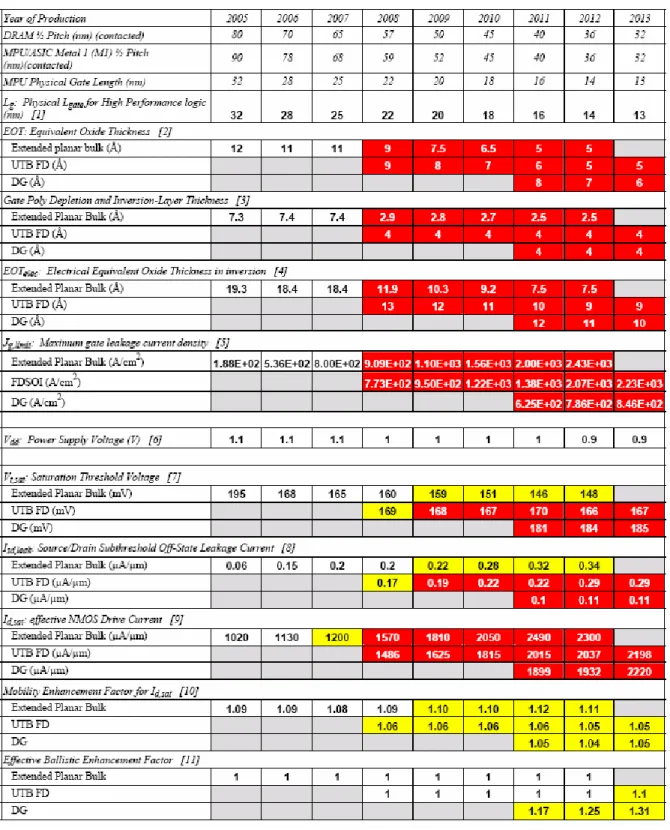
Table 1-1 High-performance Logic Technology Requirements Roadmap. ( ITRS:2005 updae )
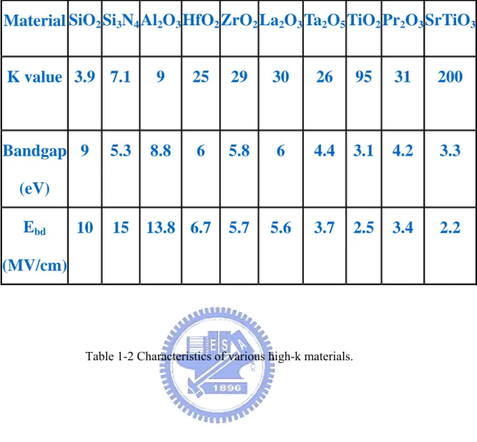
Table 1-2 Characteristics of various high-k materials.
Figure Captions
Chapter 1
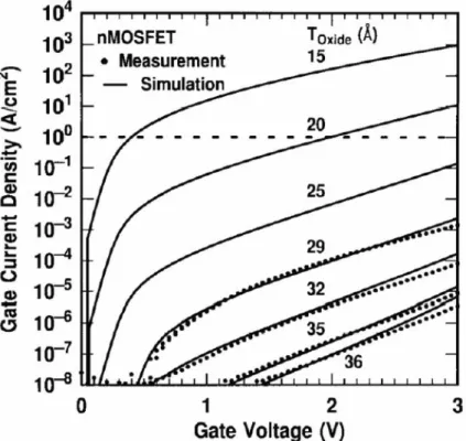
Fig. 1-1 With the marching of technology nodes, gate dielectric has to be shrunk and five silicon atoms thick of gate dielectric is predicted for 2012.[1]Fig. 1-2 Gate leakage reduction by high-k dielectric. (B-Y Nguyen, 6th TRC October 27-28, 2003 Motorola)
Fig. 1-2 Measured and simulated Ig-Vgcharacteristics under inversion condition for
nMOSFETs. The dotted line indicates the 1A/cm2
limit for the leakage current. [2]
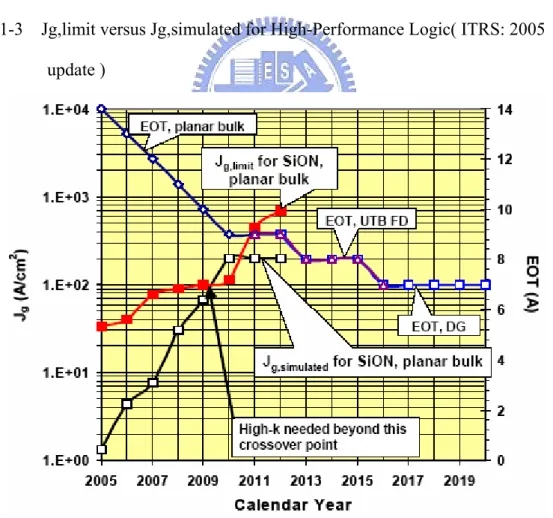
Fig 1-3 Jg,limit versus Jg,simulated for High-Performance Logic ( ITRS: 2005 update )
Fig. 1-4 Jg,limit versus Jg,simulated for Low Operating Power ( ITRS: 2005 update ) Fig. 1-5 Jg,limit versus Jg,simulated for Low Standby Power ( ITRS: 2005 update ) Fig. 1-6 Power consumption and gate leakage current density comparing to the
potential reduction in leakage current by an alternative dielectric exhibiting the same equivalent oxide thickness [3].
Fig. 1-7 Several high-k gate dielectric materials with their bandgaps and dielectric constants.[15]
Chapter 2
Fig. 2-1 The fabrication flow of this experiment.
Fig. 2-2 The ICP plasma system that was used in this experiment.
Chapter 3
Fig.3-1 The capacitance-voltage (C-V) characteristics of HfO2 gate dielectrics treated with N2 plasma treatment for different process time.
Fig.3-2 The capacitance-voltage (C-V) characteristics of HfO2 gate dielectrics treated with N2O plasma treatment for different process time.
Fig.3-2 The capacitance-voltage (C-V) characteristics of HfO2 gate dielectrics treated with O2 plasma treatment for different process time.
Fig.3-4 The capacitance-voltage (C-V) characteristics of HfO2 gate dielectrics treated
with N2 plasma treatment for 1 min, N2O plasma treatment for 10 sec, and O2
plasma treatment for 30 sec.
Fig.3-5 The J-V characteristics of p-type HfO2 capacitors treated by N2 plasma with
different process time from 0 V to -1 V.Fig. 4-7 J-V characteristics of p-type Fig. 3-6 The J-V characteristics of p-type HfO2 capacitors treated by N2O plasma with
different process time from 0 V to -1 V.
Fig. 3-7 The J-V characteristics of p-type HfO2 capacitors treated by O2 plasma
with different process time from 0 V to -1 V.
Fig. 3-8 The J-V characteristics of HfO2 gate dielectrics treated with N2 plasma
treatment for 1 min, N2O plasma treatment for 10 sec, and O2 plasma
treatment for 30 sec.
Fig. 3-9 The counts of Hf-N bonds with different conditions which are N2 for 1 min,
N2O for 10 sec, and O2 for 30 sec.
Fig. 3-10 The counts of oxygen with different conditions which are N2 for 1 min,
x
Chapter 4
Fig. 4-1 The hysteresis of p-type HfO2 gate dielectrics treated without treatment.
Fig. 4-2 The hysteresis of p-type HfO2 gate dielectrics treated with N2 plasma
treatment for different process time.
Fig. 4-3 The hysteresis of p-type HfO2 gate dielectrics treated with N2O plasma
treatment for different process time
Fig. 4-4 The hysteresis of p-type HfO2 gate dielectrics treated with O2 plasma
treatment for different process time.
Fig. 4-5 The SILC curve of p-type HfO2 gate dielectrics treated with N2 plasma
treatment for different process time.
Fig. 4-6 The SILC curve of p-type HfO2 gate dielectrics treated with N2O plasma
treatment for different process time.
Fig. 4-7 The SILC curve of p-type HfO2 gate dielectrics treated with O2 plasma
treatment for different process time.
Fig. 4-8 The SILC compare of HfO2 gate dielectrics treated with N2 plasma
treatment for 1 min, N2O plasma treatment for 10 sec, and O2 plasma
treatment for 30 sec.
Fig. 4-9 The gate current shift of p-type HfO2 gate dielectrics treated with N2
plasma treatment for different process time as a function of stress time during Vg = 1 V CVS stress.
Fig. 4-10 The gate current shift of p-type HfO2 gate dielectrics treated with N2O
plasma treatment for different process time as a function of stress time during Vg = 1 V CVS stress.
Fig. 4-11 The gate current shift of p-type HfO2 gate dielectrics treated with O2
plasma treatment for different process time as a function of stress time during Vg = 1 V CVS stress.
Fig. 4-12 The CVS compare of HfO2 gate dielectrics treated with N2 plasma
treatment for 1 min, N2O plasma treatment for 10 sec, and O2 plasma
treatment for 30 sec.
dielectrics treated with N2 plasma treatment for different process time.
Fig. 4-14 The charge-to-breakdown characteristics ( QBD ) of p-type HfO2 gate
dielectrics treated with N2O plasma treatment for different process time.
Fig. 4-15 The charge-to-breakdown characteristics ( QBD ) of p-type HfO2 gate
dielectrics treated with O2 plasma treatment for different process time.
Fig. 4-16 The charge to breakdown characteristics ( QBD ) of p-type HfO2 gate
dielectrics treated with N2 plasma treatment for 1min, N2O for 30 sec, and O2
Chapter 1
Introruction
1.1 Background
According to the famous ”Moore’s Law”, proposed by Gordon Moore in 1965, which states that the number of transistors on integrated circuits doubles every 18 months, pursuing better performance with lower cost is needed. For decades, the progress in the IC industry more or less follows this law. On the other word, ”Moore’s Law” is the basis for the overwhelmingly rapid growth of the computing power. In order to achieve the goal, the scaling down of the device dimension is an inevitable tendency.
In terms of the first order current-voltage relation, the driving current of a MOSFET can be given as
1
(
)
2 2 dsat g n GS t eff W I C V V L µ = − (1.1) g 0 inv A C t κε = (1.2)Where VGS is the applied gate to source, Leff is the effective channel length, W
the gate capacitance, κ is the dielectric constant, ε0 is the permittivity of free space
and tinv is the electrical film thickness. From the formula, we know that with
reduced threshold voltage, smaller effective channel length, and increased gate capacitance as well as gate-to-source voltage, the device can achieve better current driving ability. Of course, it can also have higher device density, which means a better
performance and much more transistors on the chip. However, a large VGS will
degrade the reliability while too small Vt
will result in statistical fluctuation in
thermal energy at a typical operation circumstance of up to 100 . So a bigger C℃ gand
shorter Leff will be needed to maintain device performance.
1.2 The Need to Use High-k Dielectric
Over the past 30 years, SiO2has served its role as a perfect gate dielectric, and
has been scaled down from a thickness of 100nm to 1.2nm at 90nm process
technology node today, in order to gain a large Cgand a higher density. In 1999,
Schulz in Nature predicted that, in order to keep up with the roadmap goal, in 2012 the thickness of gate oxide is slated to scale down to 1nm, which represents only five silicon atoms thick ( see Fig 1-1 ) [1]. Thus the direct tunneling current which depends strongly on film physical thickness will increase to an unacceptable range, resulting in a high power dissipation and heat .we can see the machine from(1.3).
( )
2 2 exp 2 DT phys mq I T h φ π ⎛ ⎞ ⎜ ⎟ ∝ − ⎜ ⎟ ⎜ ⎟ ⎝ ⎠ (1.3)2nm before exceeding the limit of 1A/cm2 from the viewpoint of allowable stand-by power dissipation. Below 2nm, however, the oxide tunneling current will quickly
becomes problematic. For easily sensing the seriousness of leakage problem: as SiO2
thickness is reduced, leakage current increases exponentially (~10×/2Å)[2]
On the other hand, we can take the view of Roadmap of gate dielectric. Fig. 1-3
shows thehigh-performance logic scaling-up of gate leakage current density limit and
of simulated gate leakage due to direct tunneling. In 2006, the EOT ( Effective Oxide Thickness ) is about 1.1 nm and the leakage current density of the oxynitride is below the leakage limit line. However, after 2008, the EOT is below 1.0 nm and the oxynitride is incapable of meeting the limit on the gate leakage current density. Fig. 1-4 shows the low operating power (LOP) scaling-up of gate leakage current density limit and simulated gate leakage due to direct tunneling. In 2006, the EOT is only 1.3 nm but the leakage current density of the oxynitride is still below the limit line because the application of high-performance logic could endure larger gate leakage current. However, after 2010, the oxynitride couldn’t be used for high-performance logic anymore. Fig. 1-5 shows the Low Standby Power scaling-up of gate leakage current density limit and simulated gate leakage due to direct tunneling. About this case we can notice that the oxynitride couldn’t be used for Low Standby Power device anymore after 2007. Table 1-1 is the roadmap of 2004 ITRS (International Technology Roadmap for Semiconductor) for the high-performance logic technology. After 2008, the requirement of EOT even reduces to less than 1 nm. It would be a big
challenge because the leakage current is too large to be acceptable for SiO2 under
such a thin thickness
Because the leakage current is related to the physical thickness of the gate oxide from (1.3), we can notice that if we make the gate dielectric thicker and still maintain
the same Cg value, the leakage current problem would be solved. This is mean that
there will be a new material to replace traditional SiO2gate dielectric. In order to
maintain the same C
g value, (1.2) can be rewritten as follows:
3.9 high k high k high k eq eq ox k k t t t k − − − = = (1.4)
where the teq term represents the theoretical thickness of SiO2. So by increasing
the gate dielectric constant, the same equivalent oxide thickness can be obtained with a thicker physical thickness, which can reduce the gate leakage current (i.e., direct
tunneling), without sacrificing the performance. Consequently, SiO2gate dielectric
needs to be replaced by the material with high dielectric constant.
1.3 The Choice of High-k Materials
High-k gate materials can maintain the same EOT with thicker physical thickness, and is therefore expected drastically reduced direct-tunneling current. From Fig1-6, the increased physical thickness significant reduces the probability of tunneling across the insulator, and hence, reduces the amount of off-state leakage current density. [3]
The relationship between dielectrics constant and thickness is followed:
(1.5)
Al2O3, Ta2O5and so on. Which one will emerge as the winner for replacing the silicon
dioxide? Since over the past three decades, SiO2has served as an ideal gate dielectric,
its several advantages, such as being amorphous phase through the whole integration processing, high quality interface, and good thermal stability, can indeed serve as a good guide of choosing high-k material. So, an ideal gate dielectric should meet the following requirements below:
1.3.1 Physical Properties
(a) Thermodynamic stability in direct contact with silicon, Preserve capacitance of gate stack after processing.
(b) Film morphology (amorphous) and stable process compatibility,
In the VLSI process, the thermal budget is an important concern since high temperature changes dielectric phase. Once the gate dielectric material has transformed to polycrystalline from amorphous phase, the large grain boundaries would serve as leakage path, and induce large leakage current. (c) Suitable high k value (12~60),
A suitable k value is indispensable. Those with not enough high k value could not satisfy (1.3) to lower the leakage by increasing physical thickness. While those with too high a k value, in general, would suffer from thermal stability issues and larger fringing field.
(d) Wide bandgap with conduction band offset > 1eV,
It is found that most of the high-k materials do not have wide enough bandgap. In contact with silicon and gate electrode, the bandgap is closely related to the barrier height for carrier transport. Too low a bandgap will lead
(e) Gate material compatibility
Materials such as metal gate, and metals have been considered for better controllability and better performance.
1.3.2 Electrical Properties
(a)Low interface state density (Dit< 5x10
10
/cm2-eV-1), and SiO2-like mobility,
The interface would affect the carrier mobility in the channel, and from (1.2), mobility degradation is related to poor current drivability. In high-k, there are so many sources that would reduce mobility, such as fixed charge, remote phonon, interfacial dipoles, remote surface roughness, surface roughness and phase separation crystallization. And most of them can be avoided by improving process technology.
(b) Tinv<1nm, (c) J<10-3A/cm2 @ V DD, (d) VFBand hysteresis < 20mV, (e) No C-V dispersion, (f) Reliability issue.
To serve as a new gate dielectric, we must also take into consideration electrical reliabilities, such as stress-induced leakage current (SILC), time dependent dielectric breakdown (TDDB), hot carrier aging, bias temperature instability and charge trapping issues [5].
There are many kinds of high-k materials, including Al2O3, Y2O3, Ta3O5, TiO2,
ZrO2 and HfO2 etc. Table 1-2 lists basic characteristics of several high-k dielectrics.
Unfortunately, many high-k materials such as Ta205, TiO2, SrTiO3, and BaSrTi03 are
thermally unstable when directly contacted with silicon [6] and need an additional barrier layer which may add process complexity and impose thickness scaling limit. Also, materials with too low or too high dielectric constant may not be adequate choice for alternative gate dielectric application. Ultra high-k materials such as STO or BST may cause fringing field induced barrier lowering effect. [7] Materials with
relatively low dielectric constant such as A12O3 and Y2O3 do not provide sufficient
advantages over SiO2 or Si3N4 [8].
Among the medium-k materials compatible with silicon, oxides of Zr and Hf are attracting much attention recently. Especially, Hf forms the most stable oxide with the highest heat of formation (∆Hf = 27l Kcal/mol) among the elements in IVA group of the periodic table (i.e. Ti, Zr, Hf). Unlike other silicides, the silicide of Hf can be
easily oxidized [9]. HfO2 possesses a dielectric constant of up to 25 [10], a large
bandgap of 5.7 eV with sufficient band offset of larger than 1.5 eV [11], and well
thermal stability in contact with silicon [12]. Fig 1.7 shows HfO2 is the most suitable
material about the struggle between dielectric constant and bandgap. HfO2 is very
resistive to impurity diffusion and intermixing at the interface because of it’s high
density (9.68 g/cm3) [13]. In addition, HfO2 is the first high-k material showing
compatibility with polysilicon gate process [14]. These properties make HfO2 one of
the most promising candidates for alternative gate dielectric application. [15]
1.4 The Challenges of High-k dielectrics
generation of sub-1.5-nm gate dielectrics. Although several groups have demonstrated in recent years the excellent electrical properties of MOS capacitors featuring
HfO2-based gate dielectrics, [16~18] there still remain many challenging issues, such
as the exists of the interfacial layer which causes the C value lower and degrades the mobility [18] in MOSFET devices. Besides these, traps in high-k gate dielectrics have been demonstrated as another issue of concern because their presence can cause threshold voltage instability [20 common 21] and a degradation in their reliability [22],
such as hysteresis caused by charge-trapping [23]. It is investigated that the reasons of
threshold voltage instability likely be Fermi-level pinning [24].The results indicate
that pinning occurs due to the interracial Si-Hf bonds for HfO2. Finally, the high
temperature of activation process introduce to thermal stability problem. For example, crystallization may let leakage current issue become worse because of providing leakage path. In brief, we summarize the challenge if High-k dielectrics as below:
(a) extra interfacial layer growing lower the C value
(b) the degradation of mobility
(c) threshold voltage instability and hysteresis issue
(d) charge-trapping issue
(e) thermal stability problem
In a word, High-k dielectrics although provide a low leakage current and satisfied C value, but the reliability issues can not be ignorable. So, it needs some
treatments to overcome these problems.
1.5 Plasma Nitridation
According to traditional view of improving SiO2 device performance, we can
find that nitridation is a common method to improve the interface. [25]Property with
the result that there is often Nit or Dit in the interface, imperfect bonding of interface
often makes the characteristic of the device deteriorate. Such as charge will be trapped by the defects of the interface, it produce flat band voltage shift and also reduce mobility. Another shortcoming is that these dangling bonds will easily bond with oxygen atom in the following high temperature environment. The extra chemical reaction will let the interfacial oxide growth, and it will reduce the C value because of the lower dielectric constant. Moreover, the quality of interfacial layer formed by oxidation is worse, and there still will be the more problems of charge trapping.
In order to solve these problems, nitridation treatment can let the atom of nitrogen bond with these dangling bonds and fix it while entering the interface layer, and then improve the stability and reliability of interface. Consequently, nitridation treatment is a workable solution to improve interface quality
As we note before, the question about using high-k materials to replace SiO2 is
that there are too many defects in the interface to cause reliability degradation. Therefore, when we use high-k materials, it is consider that nitridation treatment is a more suitable way to improve reliability and thermal stability of device. These kind of treatment have already used in some relevant references. [26] [27] Among them, someone take nitridation treatment at high temperature, others take so-called plasma
nitridation . According to [28], we can understand that the effect of plasma nitridation is better than thermal nitridation. The reason is that high-k materials are afraid of high temperature. As long as the temperature reaches certain degree, we can see phenomenon of crystallization. The crystallization of dielectric will raise leakage current substantially, because it offers the path of leahage. On the other hand, the meaning of plasma nitridation is to activate the source gas first. The high activation energy of radical will provide better mend which is better than nitridation at high temperature. For all these reasons, we adopt plasma nitridation in present experience.
1.6 Thesis Organization
Following chapters in the thesis are primarily organized as follow:
In chapter 2, we make a description of experimental details. DC magnetron sputtering system is used to deposit hafnium on silicon surface.
In chapter 3, we discuss the characteristics of ultra-thin HfO2 insulator by
Metal-Insulator-Semiconductor (MIS) capacitors.
In chapter 4, we discuss the reliability of ultra-thin HfO2 insulator by
Metal-Insulator-Semiconductor (MIS) capacitors.
In chapter 5, we make the conclusions for this thesis and provide some suggestions for future work.
Chapter 2
Experiments of Al/HfO
2/Si MIS Capacitor
2.1 MIS Capacitors Fabrication Process
In this thesis, Al/HfO2/Si MIS capacitor were fabricated to study ultra thin HfO2
gate dielectrics. Figure 2-1 shows the fabrication flow of this experiment. The starting wafer was four inch (100) orientated p-type wafer with boron doped . It was one side polished and its resistivity was 5~10 ohm-cm.
After standard initial RCA cleaning, wafers were put into chamber and grew a hafnium layer with DC magnetron sputtering system. The thickness of as-deposit hafnium thin films was 20 Å which was read by the sensor inside the sputtering
system. During sputtering, chamber pressure was maintained around 7.6×10⁻³ torr and
the flow rate of Ar was 24 standard cubic centimeters per minute (sccm). Subsequently, samples were oxidized in furnace system at 400 ℃ for 15 minutes with oxygen flow rate 5000 sccm. The reasons why we adopt this two-step method to
prepare HfO2 films will be shown at the next section 2.2.
After the HfO2 films were prepared, some samples were subjected to an
additional plasma treatment at the substrate temperature of 300 ℃while the pressure
was 100 mTorr and the plasma power was 1 W/cm2.The plasma treatment conditions
5 minute respectively and the flow rate were 100 sccm. After that, pure aluminum films were thermally evaporated on the top side of wafers.
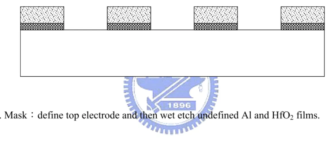
Mask defined the top electrode. Then, we used wet etching to etch undefined Al
and HfO2 films. After patterning, backside native oxide was stripped with diluted HF
solution, and Al was deposited as bottom electrode. The detailed fabrication process flow was listed as follows.
1. Initial RCA cleaning.
2. DC magnetron sputtering hafnium 20 Å.
3. Thermal oxidize hafnium in furnace in an O2 ambient at 400 ℃
for 15 minutes.
4. Plasma treatment with N2, N2O, or O2 plasma for 10 second, 30 second, 1 minute, 3
minute, or 5 minute respectively
5. Thermally evaporate 5000 Å aluminum as top electrode.
6. Mask:define top electrode and then wet etch undefined Al and HfO2 films.
7. Strip backside native oxide and coat 5000 Å aluminum as bottom electrode.
parameter analyzer (HP4156A) and C-V meas urement (HP4284) to analysis electric characteristics (i.e. I-V, C-V, EOT, leakage current density etc.). Then we tested their reliability, including stress induced leakage current (SILC), constant current stress(CCS), constant voltage stress (CVS), Hysteresis effect.
2.2 Sputtering System
There are various methods to prepare high-k thin films, such as chemical vapor
deposition (i.e. ALCVD, MOCVD, PECVD etc.) [29] [30] [31] and physical vapor
deposition (i.e. Sputtering, PLD etc.) [32]. About HfO2 films, the usual methods are
ALCVD, MOCVD and Sputtering. Comparing with these methods, we choice
sputtering system to despite HfO2 films because the advantages of the DC magnetron
sputtering are simple and cheap. In addition, the HfO2 film prepared by CVD system
easily contains organic impurities and oxygen vacancies inside. This will cause leakage current through Frenkel-Pool effect or trap assisted tunneling [33]. Less contaminants are produced by the process of the sputtering because there are no other unnecessary chemicals. However, the uniformity of the DC sputtering is worse than that of the ALCVD and the MOCVD in 12 inch diameter Si wafer. Further, sputtering
in an O2 ambient easily produces SiO2 interfacial layer. Therefore, we decide to
sputter Hf in an Ar ambient only. After pure hafnium has been deposited on Si
substrate, we put the wafer into furnace system with O2 ambient at low temperature
for oxidation. At some low temperature ( 400℃ ), Si will not react with O2 to form
the SiO2. Then, the HfO2 film is prepared without SiO2 interfacial layer.
Four inch high purity hafnium target was used to deposit thin film by DC magnetron sputtering system. The sputtering conditions were as follows. In the DC sputtering process chamber, the wafers were mounted on a face-down holder which
can rotate during deposition to increase film uniformity. The system was pumped
down to 2×10⁻⁶ torr first. This process made the chamber clean enough and thus
decreased the impurity of the deposited hafnium film. Then the deposition pressure
was controlled at 7.6 ×10⁻³ torr. Before started to deposit hafnium, the surface of the
hafnium target was treated by low power pre-sputtering cleaning for ten minutes. The inert gas source was argon (Ar) and its flow rate was 24 sccm. It has heavy atomic weight and could be served as a heavy iron to knock down the hafnium atoms on the target surface. Therefore, the hafnium atoms could be sputtered onto the wafers. The thickness of the deposited hafnium was read by the sensor inside the sputtering system. Then, the oxidation process of hafnium was performed by furnace system. The DC magnetron sputtering power was set at 100 W and the corresponding deposition rate was 0.2 Å/s. The thickness of hafnium films was 20 Å.
2.3 Furnace System
After hafnium had been deposited on silicon, we need an oxidation process to make it become hafnium dioxide. These Si wafers deposited with hafnium films were immediately loaded into furnace tube just as the sputtering process was finished. To
start with, the tube temperature was set at 400 ℃ and sufficient N2 gas was purging
continuously. After the tube temperature was stable in five minutes letter, N2 gas was
closed and O2 gas was introduced. The oxygen gas flow rate was set at 5000 (sccm).
We provided sufficient oxygen gas and proper time to oxidize these films.
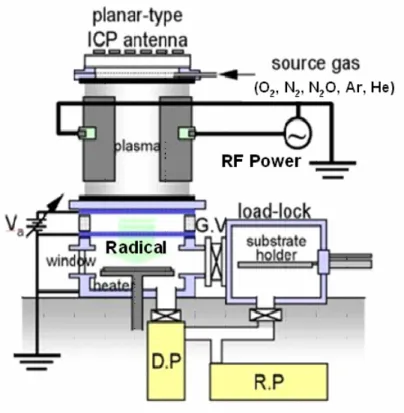
2.3 Plasma treatment system
finished, some samples were subjected to an additional plasma treatment in order to improve the electrical properties of gate dielectric. There were various source gas and
process time which were N2, N2O, or O2 plasma for 10 second, 30 second, 1 minute, 3
minute, or 5 minute as the experiment conditions. Parallel plate high-density plasma reactor employing an ICP source was a single-wafer treated and computer-controlled system.
Fig. 2.2 illustrates ICP system that was used in this experiment. 13.56 MHz RF power was coupled to the top electrode through a matching network. After the sample load to reactor, the system was pumped down to keep the chamber clean enough. Subsequently, the source gas was become radical by the plasma system, as the chamber pressure was 100 mTorr and the substrate temperature was 300℃ so that to achieve the goal of low temperature process. The power of working plasma was kept
constant at 1W/cm2 and the flow rate of source gas was 100 sccm. While the process
of plasma treatment was finished, these samples were brought to deposit Al for metal gate immediately because the effect of plasma treatment would be decrease probably.
Chapter 3
Electrical Characteristics of Al/HfO2/Si MIS
Capacitors
3.1 Capacitance-Voltage Characteristics
In order to measure the C-V characteristics of our MIS capacitors we used HP2484A LCR meter in our experiments. We swept the gate bias from inversion region to accumulation region to obtain the curve at the frequency of 10 kHz. There
are three kinds of plasma treatment with different source gas ( i.e. N2, N2O, and O2 )
and they were treated for different process time ( i.e. 10 sec, 30sec, 1min, 3min, and 5 min). Firstly, the relationship of difference process time in one kinds of plasma treatment will be discussed. Then compare with the effect of different source gas.
Fig. 3-1 reveals the capacitance-voltage (C-V) characteristics of HfO2 gate
dielectrics treated with N2 plasma treatment for different process time. The capacitor
treated for 1 minute shows the maximum capacitance among these conditions of process time. In addition, the capacitor treated for 10 second and 30 second both show the good C values which are larger then the capacitor with the condition of no
treatment. This phenomenon indicates that the N2 plasma treatment was workable to
improve the capacitance. Maybe it is caused of the intensifying of the interface structure or high-k bulk itself. The growing of interfacial oxide has also been restrained. On the other hand, the capacitance treated for 5 minute is very low and it is
even lower than the no-treated sample. It is seems that the plasma damage occur and then destroy the structure of high-k capacitance when the duration of plasma treatment is too long. The degradation of capacitance also can be found at the case of 3 min-treatment time, although the C value is still larger then the case without plasma treatment.
Fig. 3-2 shows the capacitance-voltage (C-V) characteristics of HfO2 gate
dielectrics treated with N2O plasma treatment for different process time. Just like the
group of N2 plasma treatment. The improvement of capacitance and the damage cause
by excessive plasma treatment both can be seen. At this condition, the capacitance treated with N2O plasma treatment for 10 second shows the largest value. Then, the capacitance becomes worse and worse with the increase of the treatment time. By the way, the samples besides 3 min and 5 min all perform well about larger capacitance
then the sample without treatment. It is indicated that N2O plasma treatment is also a
practicable method to improve the capacitance-voltage characteristics of HfO2 gate
dielectrics.
Fig. 3-3 shows the capacitance-voltage (C-V) characteristics of HfO2 gate
dielectrics treated with O2 plasma treatment for different process time. The
experiment of plasma treatment only with oxygen radical is wanted to see if it is still existed the improvement of capacitance, even if without nitridation. Consequently, it is shown that the capacitors treated for 10 sec and 30 ses have larger capacitances than the no-treated sample, especially for 30ses provided the maximum capacitance. Take the view of 1min condition, its capacitance has begun lower than the sample which is no treated. As the same time of 1min conditions, the other kinds of treatments still remain good capacitances then no-treated sample. So it can be know
that there are some reasons besides plasma damage occurred at the condition of 1min treatment. It is suggested that plasma treatment with oxygen radical may cause additional oxidation followed by repairing of the interface structure. Because the interfacial oxide provides lower k value, the total capacitance was be effected and become lower.
Fig. 3-4 shows the capacitance-voltage (C-V) characteristics of HfO2 gate
dielectrics treated with N2 plasma treatment for 1 min, N2O plasma treatment for 10
sec, and O2 plasma treatment for 30 sec. It is indicated that the capacitance treated
with N2 plasma treatment for 1 min shows the most excellent value ( i.e. 50%
increasing about capacitance). Among these samples, the capacitance treated with O2
plasma treatment is the worst because the growing of interfacial oxide is unavoidable while the oxygen atoms become radical and enter the interface. Besides this, the
reason why the sample treated with N2O plasma has lower capacitance then N2
plasma treatment is complex.
It is may be the growing of interfacial oxide made the capacitance degradation. Thus, the capacitance improvement by interface repair was easily eliminated by the interfacial oxide which has lower k value. So, the capacitance becomes degradation when the process time only exceeds 10 second.
3.2 Current-Voltage Characteristic
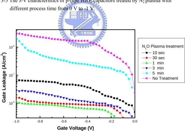
Fig. 3-5 shows the J-V characteristics of p-type HfO2 capacitors treated by N2
plasma with different process time from 0 V to -1 V. We observed that the gate leakage current density is suppressed while treatment conditions are 10sec, 30sec,
1min, and 3 min. It is indicated that N2 plasma treatment supply an effective barrier against the leakage current. The lower leakage shows that the weak structure of interface must be fixed by the plasma nitridation, especially for 1 min capacitor which both has the lowest leakage and largest capacitance value from Fig. 3.1. Gate leakage
current density of no treatment insulator at VG = 1 V is about 3.25×10⁻⁶ A/cm2. From
fig.3-5, however, gate leakage current density of the capacitor treated for 1 min N2
plasma at VG = -1 V is only about 1.35×10⁻⁸ A/cm2. It has less gate leakage than no
treatment insulator about 2 orders. Furthermore, we notices that the 3 min capacitor although has little leakage, its capacitance has become degradation. This is an interesting phenomenon. Even though the plasma damage has begun to reduce C value, the amount of leakage current is still kept very well. It means that the capacitance value is more easily affected by plasma damage than leakage current.
Fig. 3-6 shows the J-V characteristics of p-type HfO2 capacitors treated by N2O
plasma with different process time from 0 V to -1 V. After N2O plasma treatment, we can see the reduction of leakage current in contrast of no treatment samples. It is worthy to be noticed that the capacitors treated by 10 sec N2O plasma which has the
best C value also performs a low leakage current about 5.97×10⁻⁸ A/cm2. In addition,
we find that the leakage currents of 3 min and 5 min treatment are larger then 1min. But for counterpart, they are not larger then no treatment sample. Relative to the case
of N2 plasma, we can see that the level of leakage current increasing obviously
mitigate. It is possibly due to the additional oxidation layer formed by oxygen radical. The interfacial oxidation layer will let the dielectric thicker to prevent from gate leakage.
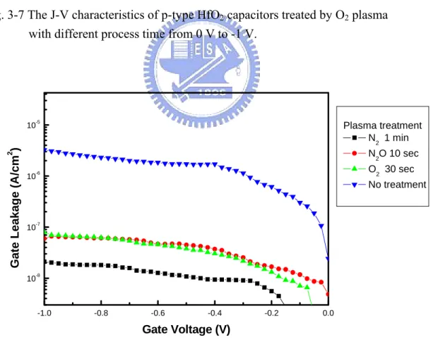
plasma with different process time from 0 V to -1 V. All of the samples depict the presence of the reduction in leakage current. It is indicated that there are not only the effect of improving interface quality but also another effect to suppress the leakage current in the case. According to the discussion about Fig. 3-3, we know that the growth of interfacial oxide layer will decrease the C value. Now the interfacial layer introduces a hard barrier to suppress leakage current. Consequently, the leakage
current all displays a lower value including the capacitor treated by O2 plasma for 5
min even if it is must be damaged by plasma.
Fig. 3-8 shows the J-V characteristics of HfO2 gate dielectrics treated with N2
plasma treatment for 1 min, N2O plasma treatment for 10 sec, and O2 plasma
treatment for 30 sec. By the compare of the samples which has the best capacitance in their own gas, we can realize the most suitable treatment condition which both has the
best capacitance and lowest leakage current. It is showed that the N2 plasma treatment
for 1 min is the best one. It is proved that without thick oxidation layer, it can also reach the smallest leakage current when there is enough long-time treatment.
3.3 Summary and SIMS profile
In order to deeply realize the effect of the plasma treatment, we take SIMS
( Secondary Ion Mass Spectrometer ) analysis to verify the phenomenon observed from CV and JV curve. Fig. 3-9 and Fig. 3-10 show the SIMS profiles of different plasma treatment conditions. Fig. 3-9 shows the counts of Hf-N bonds with different
conditions which are N2 for 1 min, N2O for 10 sec, and O2 for 30 sec. And Fig. 3-10
shows the counts of oxygen secondary ion. These three samples which show good electrical characteristic are the best process time in their own gas conditions
respectively. So we take these three samples to do SIMS analysis. First, from the Fig.
3-9 and Fig. 3-10 the sample of N2 for 1 min shows the most Hf-N bonds and the less
oxygen concentration. This explains why the sample of N2 for 1 min has the best C
value. Moreover, it is the evidence of the oxidation suppression by N2 plasma
treatment compared with no treatment sample. With the proof we can understand why
the sample of N2 for 1 min has the best C value and less leakage: the suppression of
oxidation and the Hf-N bonds which appear at the interface fix the interface structure and strengthen it.
On the other hand, although the sample of N2O for 10 sec shows a mount of
Hf-N bonds at interface, there is still oxidation at interface so that the sample shows
the less C value compared with N2 plasma treatment. However, if we take a look at
the sample of O2 for 30 sec, we can find that the oxidation phenomenon is more
serious so that its C value is the less.
As a consequence, the N2 , N2O, and O2 plasma treatment all shows better
electrical properties than no treatment sample. Furthermore, the N element and O element all can fix the interface and promote the electrical properties include of CV curve and JV curve. But for the reason of oxidation caused by oxygen radical, the
N2O and O2 plasma treatment samples shows the lower C value. Just because the
oxidation phenomenon, the films will become thicker so that the plasma damage will not easily effect the leakage current profile.
Chapter 4
Reliability of Al/HfO2/Si MIS Capacitors
4.1 Hysteresis
The name of Hysteresis was borrowed from electromagnetics. It is means that when a ferromagnetic material is magnetized in one direction, it will not relax back to zero magnetization when the applied magnetizing field is removed. It must be driven back to zero by the additional opposite direction magnetic field. If an alternating magnetic field is applied to the material, its magnetization will trace out a loop called a hysteresis loop. [34].
The hysteresis phenomenon is similar in the C-V curve of the MIS capacitor device. When we apply a voltage in opposite direction, it will not fit the original C-V curve measured previously. It is due to the traps of interface which can trap charges to influence the flat band voltage and C-V curve. [23] Fig. 4-1 shows the hysteresis of
p-type HfO2 gate dielectrics treated without plasma treatment. Fig. 4-2 shows the
hysteresis of p-type HfO2 gate dielectrics treated with N2 plasma treatment for
different process time. Hysteresis of p-type HfO2 capacitors are changed with the
increase of plasma treatment time. First, about the case of 10 sec and 30 sec we can see the hysteresis happened. When the treatment time has achieved 1min, the hysteresis is suppressed by means of the fixing ability at the interface. Until the time continues for 3 min the hysteresis becomes worse again and it attributes to plasma damage.
Fig. 4-3 shows the hysteresis of p-type HfO2 gate dielectrics treated with N2O
plasma treatment for different process time. The tendency of hysteresis is similar with
the case of N2 plasma treatment. Fig. 4-4 shows the hysteresis of p-type HfO2 gate
dielectrics treated with O2 plasma treatment for different process time. It also shows a
likely tendency. As a consequence, the plasma treatment can improve the reliability of hysteresis for the shorter process time for fear of the plasma damage brought by long
process duration. Among these samples, we can find that the hysteresis of N2 plasma
treatment for 1 min is the smallest. Therefore, we can speculate that the quality of interfacial oxide is not very well so that the charge was be trapped at the interface and introduce hysteresis.
4.2
Stress Induced Leakage Current (SILC)
In order to investigate the reliability of MIS capacitor device, the stress induced leakage current is a common experiment. The machine about SILC is the stress induced trap density in the bulk in thin film. The trap density introduce new leakage
path. Fig. 4-5 shows the SILC curve of p-type HfO2 gate dielectrics treated with N2
plasma treatment for different process time. After the stress of constant voltage ( 1V ) for 30 second, the gate leakage current become larger then before. The degree of leakage current degradation can be judged for the reliability of MIS capacitor. From Fig. 4-5, it displays the improvement of SILC compared with no-treated capacitor. Second, it is considered that the SILC of 1 min-treated sample which has the largest C value and the lowest leakage shows a very small degradation. On the other hand, it is also can be noticed that the SILC of 3 min-treated sample become worse due to the plasma damage.
Fig. 4-6 and Fig. 4-7 display the SILC curve of p-type HfO2 gate dielectrics
treated with N2O plasma treatment and O2 plasma treatment respectively. They all
show the distinct improvement as long as they are treated with plasma treatment. So
the plasma treatment including of N2, N2O, and O2 as source gas can intensify the
reliability of devices to suppress SLIC. Fig. 4-8 shows the SILC compare of HfO2
gate dielectrics treated with N2 plasma treatment for 1 min, N2O plasma treatment for
10 sec, and O2 plasma treatment for 30 sec. The sample treated by N2 plasma
treatment for 1 min shows the smallest SILC degradation because of it’s best improvement of interface quality.
4.3 Constant Voltage Stress (CVS)
To study the reliability of HfO2 film, stressing the film with a constant voltage or
a constant current are two common methods. The machine about CVS is the charge trapping by the interfacial trap density which is caused by stress for long time. Furthermore, the mount of charges cause more interface trap density and from new leakage path to add leakage. In our experiments, we use constant voltage stress (CVS)
to test the reliability of HfO2 film. Fig. 4-9 shows gate current shift of p-type HfO2
gate dielectrics treated with N2 plasma treatment for different process time as a
function of stress time during Vg = 1 V CVS stress. From the condition of 10 sec to 1min, the current shift is smaller and smaller. Then the current shift begins to become great by the damage of plasma at the process time of 3 min. Fig. 4-10 shows gate
current shift of p-type HfO2 gate dielectrics treated with N2O plasma treatment for
different process time as a function of stress time during Vg = 1 V CVS stress. It has
similar behavior about the trend. Fig. 4-11 shows gate current shift of p-type HfO2
function of stress time during Vg = 1 V CVS stress. While the 30-sec treated sample presents the lowest current shift, the 1-min treated sample become to be destroyed by
the plasma damage. Fig. 4-12 shows the CVS compare of HfO2 gate dielectrics
treated with N2 plasma treatment for 1 min, N2O plasma treatment for 10 sec, and O2
plasma treatment for 30 sec. It is verified that the sample using by N2 plasma
treatment for 1 min has the best quality of thin film.
4.4
Charge to Breakdown ( Q
BD)
Another important issue of reliability is to investigate the breakdown behavior of the gate dielectrics. As long as we inject large number of charge by the stress at constant voltage or constant current for a long period, we can find the breakdown
profile and calculate the count of QBD.
Fig. 4-13 shows the charge-to-breakdown characteristics ( QBD ) of p-type HfO2
gate dielectrics treated with N2 plasma treatment for different process time. The
charge to breakdown characteristics was measured at a constant current of -1 A/cm2.
As we respect, the capacitor treated for 1 min shows the larger QBD and it means that
the capacitor more hardly begins to breakdown. Fig. 4-14 shows the charge-to
breakdown-characteristics ( QBD ) of p-type HfO2 gate dielectrics treated with N2O
plasma treatment for different process time. Although the capacitor treated for 10
second shows the largest QBD, the capacitor treated for 1 min has become degradation.
Fig. 4-15 shows the charge-to-breakdown characteristics ( QBD ) of p-type HfO2 gate
dielectrics treated with O2 plasma treatment for different process time. Like CVS
curve, the capacitor treated for 30 sec shows the best characteristics compared to other process time. And then, we try to compare the three plasma treatment process of
different source gas. Fig. 4-16 shows the charge to breakdown characteristics ( QBD )
of p-type HfO2 gate dielectrics treated with N2 plasma treatment for 1min, N2O for 30
sec, and O2 for 30 sec. It is indicated that the sample of N2 plasma has larger QBD then
that of other plasma treatment. We thought that it is because of well structure of
interface fixed by N2 plasma for a long time.
Chapter 5
Conclusions and future work
5.1
Conclusions
In this thesis, we performed the post-deposition plasma treatment
to enrich the HfO2 film quality. The plasma treatment conditions are N2, N2O, and O2
plasma for 10 sec, 30 sec, 1 min, 3 min, 5 min individually. Several important phenomena were observed and summarized as follows.
First of all, improvement in the electrical characteristics of Al/HfO2/Si MIS
capacitors using plasma treatment has been demonstrated in this work. ALL of the plasma treatment can promote the electrical characteristics and reliability until the
plasma damage happened. Among these treatments, the sample using N2 plasma for 1
min represents a fairly great improvement, such as good capacitance ( 50% increasing ), reduced leakage current ( 2 order reduction ). It is showed that the
formation of interfacial layer has been suppressed and the weak structure of interface
has been repaired by N2 plasma respectively. With the analysis of SIMS profile, it can
be demonstrated. Besides, the sample treated by N2 plasma for 1 min also shows an
excellence promotion about reliability issue, such as smaller hysteresis ( < 1 mV ),
less SILC, better CVS curve, and larger QBD. These advancements were ascribed to
the good interface quality.
On the other hand, the N2O and O2 plasma treatment also provide a good effect
on electrical characteristics although most samples are still worse than that of N2
plasma treatment. The reason is that the samples using N2O and O2 plasma treatment
will introduce oxygen bonding to from additional interfacial layer so that the capacitance will be decreased. But for another hand, the thicker oxidation layer becomes a good resistance against leakage current even if the plasma damage has begun to occur. Therefore, we can find that these samples show lower leakage current at the process conditions of 3 min and 5 min even if their capacitance has been seriously degraded by plasma damage.
Finally, in this thesis, the point we focus on is the improvement of capacitance.
The treatment of N2 plasma for 1 min is the best condition because the capacitance has
50% increasing. Simultaneously, its reliability also represents a excellent progress. The most suitable way for post -deposition treatment by plasma to improve electrical characteristics on MIS structure is observed
5.2
Future work
the future, the ALCVD ( Atomic Layer CVD ) system will become another important deposition technology. Further experiment and analysis are required to clarify if the treatment condition is also suitable for ALCVD film. On the other hand, the MOSFET will be fabricated by the same treatment condition to verify the effect on device characteristics, such as mobility, subthreshold swing, and transonductance.
References
[1] Max Schulz, “The end of the road for silicon,” Nature, Vol. 399, pp. 729, 1999.
[2] S. –H. Lo, D. A. Buchanan, Y. Taur, W. Wang, “Quantum-Mechnical Modeling of Electron Tunneling Current from the Inversion Layer of Ultra-Thin Oxide nMOSFET’s,” IEEE Electron Device Lett., Vol. 18, pp.209, 199
[3] G. D. Wilk, R. M. Wallace, et. al., “High-k gate dielectrics: current status and materials properties consideration” J. Appl. Phys., Vol. 89, No. 10, pp. 5243, 2001.
[4] J. Robertson, J. Vac. Sci. Technol. B 18, pp1785, 2000.
[5] Robert M. Wallace, IRPS Tutorial, IRPS, 2004.
[7] Baohong Cheng, Min Cao, Ramgopal Rao, Anand Inani, Paul Vande Voorde, Wayne M. Greene, Johannes M. C. Stork, Zhiping Yu, Peter M. Zeitzoff, Jason C.S. Woo, “The Impact of High-k Gate Dielectrics and Metal Gate Electrodes on Sub-100 nm MOSFET’s”, IEEE Transactions on Electron Devices, Vol. 46, No. 7, July, 1999.
[8] C. T. Liu, “Circuit Requirement and Integration Challenges of Thin Gate Dielectrics for Ultra Small MOSFET’s”, IEDM Tech. Dig., p.747, 1998.
[9] S. P. Muraka and C. C. Chang, Appl. Phys. Lett. 37,639, 1980.
[10] M. Balog, M. Schieber,M. Michman, and S. Patai, “Chemical vapor deposition and characterization of HfO2 films from organo-hafnium compounds,” Thin Solid Films, vol. 41, pp. 247–259, 1977.
[11] J. Robertson, “Band offsets of wide-band-gap oxides and implications for future electronic devices,” J. Vac. Sci. Technol. B, vol. 18, pp. 1785–1791, 2000.
[12] K. J. Hubbard and D. G. Schlom, “Thermodynamic stability of binary oxides in contact with silicon,” J. Mat. Res., vol. 11, pp. 2757–2776, 1996.
[13] M. Balog et al. Thin Solid Films, ~01.41, 247, 1977.
[14] K. Onishi, C. S. Kang, R. Choi, H.-J. Cho, S. Gopalan, R. Nieh, S. Krishnan, and
J. C. Lee, “Effects of high-temperature forming gas anneal on HfO2 MOSFET
[15]J. Robertson, J. Vac. Sci. Technol. B 18, pp1785, 2000.
[16] B. Tavel, X. Garros, T. Skotnicki, F. Martin, C. Leroux, D. Bensahel, M. N. Se’me’ria, Y. Morand, J. F. Damlencourt, S. Descombes, F. Leverd, Y. Le-Friec, P. Leduc, M. Rivoire, S. Jullian and R. Pantel: Int. Electron Device Meet. Tech. Dig., p. 429, 2002.
[17] C. H. Choi, S. J. Rhee, T. S. Jeon, N. Lu, J. H. Sim, R. Clark, M. Niwa and D. L. Kwong: Int. Electron Device Meet. Tech. Dig., p. 857, 2002.
[18] S. Pidin, Y. Morisaki, Y. Sugita, T. Aoyama, K. Irino, T. Nakamura and T. Sugii: Symp. VLSI Tech. Dig., p. 28, 2002.
[19] J.-P Han, E. M. Vogel, E. P. Gusev, ”Energy Distribution of Interface Traps in High-k Gated MOSFETs”, VLSI, 2003.
[20] S. Zafar, A. Callegari, E. Gusev and M. V. Fischetti: J. Appl. Phys. 93, 9298, 2003.
[21] L.Pantisano, E.Cartier “Dynamics of Threshold Voltage Instability in Stacked High-k Dielectrics: Role of the interfacial Oxide”, VLSI, 2003.
[22] W. Y. Loh, B. J. Cho, M. S. Joo, M. F. Li, D. S. H. Chan, S. Mathew and D. L. Kwong: Int. Electron Device Meet. Tech. Dig.,
[23] Hokyung Park, M.Shahriar Rahman, Man Chang, Byoung Hun Lee, Rino Choi,” Improved interface Quality and Charge-Trapping Characteristics of MOSFETs With High-k Gate Dielectric”, IEEE Electron Device Letters, VOL. 26, NO. 10, October, 2005.
[24] Christopher C. Hobbs, Leonardo R. C. Fonseca,” Fermi-Level Pinning at the Polysilicon/Meal Oxide Interface-Part 1”, IEEE Electron Device Letters, VOL. 51,NO. 6, June, 2004.
[25] H.-H Tseng,Y. Jeon, P. Abramowitz, T.-Y. Luo, “Ultra-Thin Decoupled Plasma Nitridation (DPN) Oxynitride Gate Dielectric for 80-nm Advanced Technology “, IEEE Electron Device Letters, VOL. 23, NO. 12, December, 2002.
[26] Seiji Inumiya, Katauyuki Sekine, Shoko Niwa, Akio Kaneko, Motoyuki Sato,” Fabrication of HFSION Gate Dielectrics by Plasma Oxidation and Nitridation, Optimized for 65 nm node Low Power CMOS Applications ”, VLSI, 2003.
[27] Satoshi Kamiyama, Tomonori,” Improvement in the uniformity and the thermal stability of Hf-silicate gate dielectric by plasma-nitridation”, IWGI, 2003.
[28] Katsuyuki Sekine, Seiji Inumiya, Motoyuki Sato, Yoshitaka Tsunashima, “Nitrogen Profile Control by Plasma Nitridation Technique for Poly-Si Gate HfSiON CMOSFET with Excellent interface property and Ultra-low Leakage Current”, IEDM 03-103
Film Formation for MOSCAPs and nMOSFETs through Layer-by-Layer Deposition and Annealing Process ”, VLSI, 2003.
[30] T. Watanabe, M. Takayanagi, “ Design Guideline of HfSiON Gate Dielectric for 65 nm CMOS Generation ”, VLSI, 2003.
[31] Katsuyuki Sekine, Yuji Saito, Masaki Hirayama, “Highly Robust Ultrathin Silicon Nitride Films Grown at Low-Temperature by Microwave-Excitation High-Density Plasma for Giga Scale Integration”, IEEE Electron Device Letters, VOL. 47, NO. 7, JULY, 2000.
[32] Yoshitaka Nagasato, Tomo Ueno, ”Novel Fabrication Process for HfO2 Thin
Film for Gate Dielectric”, The Japan Society of Applied Physics.
[33] Wai Shing Lau, Thiam Siew Tan, Nathan P. Sandler, Barry S. Page,“Characterization of Defect States Responsible for Leakage Current in Tantalum Pentoxide Films for Very-High-Density Dynamic Random Access Memory (DRAM) Applications”, Jpn. J. Appl. Phys., Vol.34, pp.757-761, 1995. [34] HyperPhysics, C.R Nave Georgia University, 2002.
Table 1-1 High-performance Logic Technology Requirements Roadmap. ( ITRS:2005 updae )
Material
SiO
2Si
3N
4Al
2O
3HfO
2ZrO
2La
2O
3Ta
2O
5TiO
2Pr
2O
3SrTiO
3K value
3.9 7.1
9
25
29
30
26
95
31
200
Bandgap
(eV)
9
5.3
8.8
6
5.8
6
4.4
3.1
4.2
3.3
E
bd(MV/cm)
10
15
13.8 6.7
5.7
5.6
3.7
2.5
3.4
2.2
Figure-chapter 1
Fig. 1-1 With the marching of technology nodes, gate dielectric has to be shrunk and five silicon atoms thick of gate dielectric is predicted for 2012.[1]
Fig. 1-2 Measured and simulated Ig-Vgcharacteristics under inversion condition for
nMOSFETs. The dotted line indicates the 1A/cm2 limit for the leakage
Fig. 1-3 Jg,limit versus Jg,simulated for High-Performance Logic( ITRS: 2005 update )
Fig. 1-4 Jg,limit versus Jg,simulated for Low Operating Power ( ITRS: 2005 update )
Fig. 1-5 Jg,limit versus Jg,simulated for Low Standby Power ( ITRS: 2005 update )
Fig. 1-6 Power consumption and gate leakage current density comparing to the potential reduction in leakage current by an alternative dielectric exhibiting the same equivalent oxide thickness [3].
Fig. 1-7 Several high-k gate dielectric materials with their bandgaps and dielectric constants.[15]
Figure-chapter 2
1. Initial RCA cleaning.
2. DC magnetron sputtering hafnium 20 Å.
3. Thermal oxidize hafnium in furnace in an O2 ambient at 400 ℃ for 15 minutes to
4. Plasma treatment with N2, N2O, or O2 plasma for 10 second, 30 second, 1 minute, 3 minute, or 5 minute respectively
5. Thermally evaporate 5000 Å aluminum as top electrode.
6. Mask:define top electrode and then wet etch undefined Al and HfO2 films.
7. Strip backside native oxide and coat 5000 Å aluminum as bottom electrode.
Figure-chapter 3
-2.0 -1.5 -1.0 -0.5 0.0 0.5 1.0 0.0 0.1 0.2 0.3 0.4 0.5 0.6 0.7 0.8 0.9 1.0 1.1 C (uF/ c m 2 ) Voltage (V) N 2 10s N2 30s N 2 1min N2 3min N 2 5min NO TREATMENTFig.3-1 The capacitance-voltage (C-V) characteristics of HfO2 gate dielectrics treated
with N2 plasma treatment for different process time.
-2.0 -1.5 -1.0 -0.5 0.0 0.0 0.2 0.4 0.6 0.8 1.0 C (u F /cm 2 ) Voltage (V) N 2O 10s N2O 30s N 2O 1min N 2O 3min N2O 5min NO TREATMENT
Fig.3-2 The capacitance-voltage (C-V) characteristics of HfO2 gate dielectrics treated
-2.0 -1.5 -1.0 -0.5 0.0 0.0 0.2 0.4 0.6 0.8 C (F/ c m 2 ) Voltage (V) O 2 10s O2 30s O2 1min O 2 3min O 2 5min NO TREATMENT
Fig.3-2 The capacitance-voltage (C-V) characteristics of HfO2 gate dielectrics treated
with O2 plasma treatment for different process time.
-2.0 -1.5 -1.0 -0.5 0.0 0.0 0.2 0.4 0.6 0.8 1.0 C (u F/ cm 2 ) Voltage (V) N 2 1min N 2O 10s O2 30s NO TREATMENT
Fig.3-4 The capacitance-voltage (C-V) characteristics of HfO2 gate dielectrics treated
with N2 plasma treatment for 1 min, N2O plasma treatment for 10 sec, and O2
-1.0 -0.8 -0.6 -0.4 -0.2 0.0 10-8 10-7 10-6 10-5 Gate L ea kag e (A /cm 2 ) Gate Voltage (V) N 2 Plasma treatment 10 sec 30 sec 1 min 3 min 5 min No Treatment
Fig. 3-5 The J-V characteristics of p-type HfO2 capacitors treated by N2 plasma with
different process time from 0 V to -1 V.
-1.0 -0.8 -0.6 -0.4 -0.2 0.0 10-8 10-7 10-6 Gat e Le akag e (A /c m 2 ) Gate Voltage (V) N2O Plasma treatment 10 sec 30 sec 1 min 3 min 5 min No Treatment
Fig. 3-6 The J-V characteristics of p-type HfO2 capacitors treated by N2O plasma with
-1.0 -0.8 -0.6 -0.4 -0.2 0.0 10-8 10-7 10-6 G at e L e ak ag e (A /cm 2 ) Gate Voltage (V) O 2 Plasma treatment 10 sec 30 sec 1 min 3 min 5 min No Treatment
Fig. 3-7 The J-V characteristics of p-type HfO2 capacitors treated by O2 plasma
with different process time from 0 V to -1 V.
-1.0 -0.8 -0.6 -0.4 -0.2 0.0 10-8 10-7 10-6 10-5 Gate Le akag e (A /c m 2 ) Gate Voltage (V) Plasma treatment N 2 1 min N 2O 10 sec O 2 30 sec No treatment
Fig. 3-8 The J-V characteristics of HfO2 gate dielectrics treated with N2 plasma
treatment for 1 min, N2O plasma treatment for 10 sec, and O2 plasma
0 5 10 15 20 25 0.0 5.0x101 1.0x10² 1.5x10² 2.0x10² 2.5x10² 3.0x10² 3.5x10² 4.0x10² Hf-N + N N 2 1 min N2O 10 sec O2 30 sec origin Int e nsit y ( counts ) Depth ( nm )
Fig. 3-9 The counts of Hf-N bonds with different conditions which are N2 for 1 min,
N2O for 10 sec, and O2 for 30 sec.
0 5 10 15 20 25 0.0 2.0x10² 4.0x10² 6.0x10² 8.0x10² 1.0x10³ 1.2x10³ 1.4x10³ O N2 1 min N2O 10 sec O2 30 sec origin Intens it y ( counts ) Depth ( nm )
Fig. 3-9 The counts of oxygen with different conditions which are N2 for 1 min,
Figure-chapter 4
-2.0 -1.5 -1.0 -0.5 0.0 0.0 0.2 0.4 0.6 0.8 1.0 C / C MA X Voltage (V) No treatment -2 V to 0 V 0 V to -2 V hysteresis = 100 mV-2.0 -1.5 -1.0 -0.5 0.0 0.0 0.2 0.4 0.6 0.8 1.0 hysteresis = 70 mV C / C MA X Voltage (V) N2 10 sec -2 V to 0 V 0 V to -2 V -2.0 -1.5 -1.0 -0.5 0.0 0.0 0.2 0.4 0.6 0.8 1.0 hysteresis = 50 mV C / C MA X Voltage (V) N2 30 sec -2 V to 0 V 0 V to -2 V -2.0 -1.5 -1.0 -0.5 0.0 0.0 0.2 0.4 0.6 0.8 1.0 hysteresis <1 mV C / C MA X Voltage (V) N2 1 min -2 V to 0 V 0 V to -2 V -2.0 -1.5 -1.0 -0.5 0.0 0.0 0.2 0.4 0.6 0.8 1.0 hysteresis = 120 mV C / C MA X Voltage (V) N2 3 min -2 V to 0 V 0 V to -2 V
Fig. 4-2 The hysteresis of p-type HfO2 gate dielectrics treated with N2 plasma
-2.0 -1.5 -1.0 -0.5 0.0 0.0 0.2 0.4 0.6 0.8 1.0 hysteresis = 30 mV C / C MAX Voltage (V) N2 O 10 sec -2 V to 0 V 0 V to -2 V -2.0 -1.5 -1.0 -0.5 0.0 0.0 0.2 0.4 0.6 0.8 1.0 hysteresis = 50 mV C / C MA X Voltage (V) N2 O 30 sec -2 V to 0 V 0 V to -2 V -2.0 -1.5 -1.0 -0.5 0.0 0.0 0.2 0.4 0.6 0.8 1.0 hysteresis = 70 mV C / C MA X Voltage (V) N2 O 1 min -2 V to 0 V 0 V to -2 V -2.0 -1.5 -1.0 -0.5 0.0 0.0 0.2 0.4 0.6 0.8 1.0 hysteresis = 200 mV C / C MA X Voltage (V) N2 O 3 min -2 V to 0 V 0 V to -2 V
Fig. 4-3 The hysteresis of p-type HfO2 gate dielectrics treated with N2O plasma
![Fig. 1-6 Power consumption and gate leakage current density comparing to the potential reduction in leakage current by an alternative dielectric exhibiting the same equivalent oxide thickness [3]](https://thumb-ap.123doks.com/thumbv2/9libinfo/8568396.188725/51.892.160.732.535.1025/consumption-comparing-reduction-alternative-dielectric-exhibiting-equivalent-thickness.webp)
![Fig. 1-7 Several high-k gate dielectric materials with their bandgaps and dielectric constants.[15]](https://thumb-ap.123doks.com/thumbv2/9libinfo/8568396.188725/52.892.131.784.153.721/fig-high-gate-dielectric-materials-bandgaps-dielectric-constants.webp)