國 立 交 通 大 學
電信工程學系
碩 士 論 文
使用三倍頻器產生本地震盪訊號
的升頻混波器
Up-Conversion Mixer Using Frequency
Tripler for Local Oscillator Signal Generation
研究生:陳煥昇
指導教授:郭建男、鍾世忠 教授
使用三倍頻器產生本地震盪訊號的升頻混波器
Up-Conversion Mixer Using Frequency Tripler
for Local Oscillator Signal Generation
研 究 生:陳煥昇 Student:Huan-Sheng Chen
指導教授:郭建男、鍾世忠 Advisor:Chien-Nan Kuo
Shyh-Jong Chung
國 立 交 通 大 學
電信工程學系
碩 士 論 文
A ThesisSubmitted to Department of Communication Engineering College of Electrical Engineering and Computer Science
National Chiao Tung University in partial Fulfillment of the Requirements
for the Degree of Master
in
Communication Engineering July 2008
Hsinchu, Taiwan, Republic of China
I
使用三倍頻器產生本地震盪訊號的升頻混波器
學生 : 陳煥昇 共同指導教授 : 郭建男 教授
指導教授 : 鍾世忠 教授
國立交通大學
電信工程學系碩士班
摘要
本論文主要在於設計一個能提供足夠寬的中頻頻寬的升頻混波器,以應用在 60-GHz 頻段來達到高資料量傳輸的目的。此升頻混波器使用一個三倍頻器來提 供其本地震盪訊號。此外,又特別針對三倍頻器提出了新的架構,經由仔細的分 析,此三倍頻器能更有效地產生三倍頻的訊號。 在本論文中共實現兩顆晶片,第一顆晶片為具有寬的中頻頻寬的升頻混波 器,使用TSMC 0.13-μm CMOS 製程。量測結果顯示其在 2.7 mW 的功率耗損 下,有-5.6 dB 的轉換增益,並提供了 3.5 GHz 的中頻頻寬,使其適用於高速資 料傳輸。 第二顆晶片為所提出的次諧波電流注入式三倍頻器,使用 TSMC 0.18-μm CMOS 製程。模擬結果顯示其在僅 2.6 mW 的動態功率耗損下,有-5.7 dB 的轉換 增益。此外,此三倍頻器能有效地鎖定I/Q 訊號的不均衡,使其在通訊系統整合 上具有相當的潛力。II
Up-Conversion Mixer Using Frequency Tripler for Local
Oscillator Signal Generation
Student : Huan-Sheng Chen Joint Advisor : Chien-Nan Kuo Advisor : Shyh-Jong Chung
Department of Communication Engineering
National Chiao-Tung University
ABSTRACT
This thesis aims at the design of an up-conversion mixer with wide intermediate frequency (IF) bandwidth for providing high data-rate transmission at 60-GHz band. A frequency tripler is used to provide local oscillator signal for the up-conversion mixer. In addition, we propose a novel structure for frequency tripler. Through detailed analysis, this proposed frequency tripler can generate the third-order harmonic efficiently.
Two chips are realized in this thesis. In the first chip, an up-conversion mixer with wide IF bandwidth is fabricated using TSMC 0.13-μm CMOS technology. Experimental results show -5.6dB conversion gain and 3.5-GHz IF bandwidth under 2.7mW power consumption, which is feasible for high-speed data transmission.
In the second chip, the proposed harmonic current injection frequency tripler is fabricated using TSMC 0.13-μm CMOS technology. Simulation results show -5.7 dB conversion gain under only 2.6 mW dynamic power consumption. In addition, this frequency tripler can lock the input I/Q imbalance, which makes its great potential in the integration of communication systems.
III
誌 謝
得以順利完成本篇論文,首先要感謝的是我的兩位指導教授,郭建男教授與 鍾世忠教授。在鍾世忠教授前半年的悉心指導下對微波領域有所瞭解,往後一年 半更在郭建男教授的竭力指導下學習到嚴謹的研究態度與具邏輯的分析方法,在 此向兩位老師致上深深的敬意。 感謝昶綜、鈞琳、明清、鴻源等學長們的不吝指導,在研究上給予我許多的 幫助與提供許多想法。另外,要感謝ICS 實驗室的旻珓、柏宏學長在研究方向與 晶片量測上的協助。 感謝和我一起做研究、一同奮鬥、互相勉勵的易耕,以及 子超、俊豪、建忠等學弟們,和你們一起學習、熬夜、打球、吃美食,在我的碩 士生活中留下許多難忘的回憶。此外,感謝我的朋友家豪,借了我液晶螢幕,使 得我能夠在下定決心的那天起便開始全力撰寫論文,不至使鬥志消退。感謝國家 系統晶片中心在晶片製作上所提供的協助。 最後,要特別感謝我的父母與家人的栽培與鼓勵,以及女友毓瑜在精神上的 默默支持,因為你們相信我,我才能一直走下去。 陳煥昇 九十七年八月IV
CONTENTS
Abstract (Chinese)………..I
Abstract (English)……….II
Acknowledgements………..III
Contents………IV
Table Captions………VII
Figure Captions………VIII
Chapter 1 Introduction……….………1
1.1 Background and Motivation………...1
1.2 Thesis Organization………2
Chapter 2 Fundamentals in Nonlinear Circuit Design……...3
2.1 Linearity and Nonlinearity………..3
2.2 Nonlinear Phenomena……….4
2.2.1 Harmonic Generation………...4
2.2.2 Intermodulation Distortion………...5
2.2.3 Saturation and Desensitization……….6
2.2.4 AM-to-PM Distortion………...6
2.3 Harmonic Balance Analysis………7
Chapter 3 60-GHz Up-Conversion Mixer with Wide IF
Bandwidth………..12
3.1
Introduction……….12
V
3.2 Analysis on Impedance Using Large-signal Method…………14
3.3 Circuit Realization………21
3.3.1 Direct Up-Conversion Mixer……….22
3.3.2 Marchand-type Balun……….25
3.3.3 Injection-locked Frequency Tripler………26
3.4 Experimental Results………27
3.5 Summary………...38
Chapter 4 Frequency Tripler Using Second-Order Current
Injection Technique………...…39
4.1 Introduction………...39
4.2 Second-order Current Injection………41
4.2.1 Output Current versus Injection Phase………...44
4.2.2 Injection Node………49
4.2.3 Optimal Injection Phase Calculation………..52
4.2.4 Injection-to-Bias Ratio………...60
4.2.5 Second-order Current Generation………..65
4.2.6 Input to Output I/Q Imbalance………...69
4.3 Measurement Considerations………....70
4.4
Chip Implementation……….73
4.5 Summary………...81
Chapter 5 Conclusion and Future Work………...82
5.1 Conclusion………82
5.2 Future Work………..82
VI
VII
TABLE CAPTIONS
Table 3.1 Comparison with published up-conversion mixers……….38
VIII
FIGURE CAPTIONS
Fig. 2.1 A simple dc-biased diode………...8
Fig. 2.2 A diode excited by an RF circuit (a) can be divided into a pair of equivalent circuits, one describing the linear part (b), and another, the nonlinear part (c)…..10
Fig. 3.1 The operational concept of HB method and time-domain method………..15
Fig. 3.2 Actual signal and signal assumed by FFT………16
Fig. 3.3 Circuit for establishing the method to observe the impedance………17
Fig. 3.4 Simulated input impedance (100 MHz ~ 10 GHz) without LO swing……18
Fig. 3.5 The corresponding return loss without LO swing………19
Fig. 3.6 Simulated input impedance (100 MHz ~ 10 GHz) with 0.4-Vpp LO swing………....19
Fig. 3.7 The corresponding return loss with 0.4-Vpp LO swing………20
Fig. 3.8 Architecture of the fabricated circuits………….……….21
Fig. 3.9 Schematic of the proposed up-conversion mixer……….22
Fig. 3.10 Simplified circuit for choosing appropriate bias current………..23
Fig. 3.11 Normalized conversion gain versus bias current………..24
Fig. 3.12 The corresponding VGS at switching stage………...24
Fig. 3.13 3-D view of Marchand-type balun………...25
Fig. 3.14 Simulated gain difference before/after Marchand-type balun………..26
Fig. 3.15 Schematic of injection-locked frequency tripler………..27
Fig. 3.16 Chip micrograph………...28
Fig. 3.17 Measurement setup………...29
Fig. 3.18 Measured frequency response of up-conversion mixer and frequency tripler………30
IX
Fig. 3.19 Simulated frequency response of ILFT………30
Fig. 3.20 Measured output spectrum under -25 dBm IF input power……….31
Fig. 3.21 Measured input 1-dB compression point of up-conversion mixer………...31
Fig. 3.22 Measured input third-order intercept point of up-conversion mixer………32
Fig. 3.23 Measured output spectrum under -15dBm IF input power………..32
Fig. 3.24 Measured IF bandwidth of up-conversion mixer……….34
Fig. 3.25 Measured IF port matching………..35
Fig. 3.26 Measured IF port matching at 0-dBm LO power……….35
Fig. 3.27 Measured RF port matching at 0-dBm LO power………36
Fig. 3.28 Measured output waveform at IF frequency of 1GHz and LO frequency of 61.2GHz………...37
Fig. 3.29 Measured output waveform at IF frequency of 1GHz and LO frequency of 61.2GHz (close-in)………...37
Fig. 4.1 Block diagram of generating third-order harmonic………..41
Fig. 4.2 The straightforward implementation of our idea………..41
Fig. 4.3 A source-coupled pair………...42
Fig. 4.4 Simplified circuit………..42
Fig. 4.5 (a) Fully-simplified circuit and its (b) conceptual circuit……….43
Fig. 4.6 Further simplified for analyzing………...44
Fig. 4.7 Normalized output current – (a) the fundamental (b) the second-order (c) the third-order………...45
Fig. 4.8 Conceptual circuit partition………..47
Fig. 4.9 Normalized (a) overall output third-order current and output third-order current without current injection (b) injected contribution in complex plane……….48
X
Fig. 4.11 second-order harmonic voltage of Vm (a) without (b) with second-order
current injection………49 Fig. 4.12 Normalized third-order output current under different injection level…….50 Fig. 4.13 Normalized third-order output current under different injection level in
complex plane………..51 Fig. 4.14 Normalized (a) Gm1 (b) Gm2 (c) Gm3 under various gate biases…………...54
Fig. 4.15 Normalized (a) Gm1 (b) Gm2 (c) Gm3 under various gate biases and
Frequencies………...55 Fig. 4.16 Normalized (a) calculated and (b) simulated output third-order current
excited by the injection current………60 Fig. 4.17 Normalized magnitude of the third-order output current versus injection
phase from α=0 to α=0.4………..61 Fig. 4.18 Normalized third-order output current versus injection phase in complex
plane from α=0 to α=0.4………...62 Fig. 4.19 Normalized magnitude of third-order output current versus injection phase
from Ibias=1mA to Ibias=3mA……….63
Fig. 4.20 Normalized third-order output current versus injection phase in complex
plane from Ibias=1mA to Ibias=3mA………...63
Fig. 4.21 HRR1 versus Ibias and α……….64
Fig. 4.22 HRR2 versus Ibias and α……….64
Fig. 4.23 Conceptual time-domain waveform of fundamental input voltage at upper differential pair (in gray) and second-order injection current (in black) (not to scale)………65 Fig. 4.24 (a) The lower differential pair (b) conceptual time-domain waveform of
fundamental input voltage at the lower differential pair (in gray) and the desired second-order injection current (in black) (not to scale)…………...66
XI
Fig. 4.25 Needed fundamental voltage waveforms……….67
Fig. 4.26 The proposed HCI-FT………..68
Fig. 4.27 The proposed I/Q HCI-FTs………..68
Fig. 4.28 Simulated input to output I/Q imbalance……….69
Fig. 4.29 Comparison of HCI-FT and conventional method………...70
Fig. 4.30 On-chip Marchand balun (a) front view (b) back view………71
Fig. 4.31 Simulated (a) magnitude (b) phase response of Marchand balun within 2 GHz to 30 GHz………..72
Fig. 4.32 Simulated magnitude error and phase error within 4GHz to 12GHz……...72
Fig. 4.33 Block diagram of fabricated HCI-FTs………..73
Fig. 4.34 Schematic of fabricated HCI-FTs……….74
Fig. 4.35 Layout of the fabricated circuits………...75
Fig. 4.36 The corresponding circuit diagram………...75
Fig. 4.37 Simulated conversion gain versus frequency………...76
Fig. 4.38 Simulated conversion gain versus device (width) mismatch………...76
Fig. 4.39 Simulated HRRs versus frequency………...77
Fig. 4.40 Simulated output voltage swing versus input voltage swing of HCI-FT with input frequency of 8 GHz……….77
Fig. 4.41 Simulated HCI-FT output I/Q waveforms with input frequency of 8 GHz ………..78
Fig. 4.42 Simulated HCI-FT output differential waveforms with input frequency of 8 GHz………..78
Fig. 4.43 Simulated fundamental input waveform and the third-order output Waveform……….79
1
Chapter 1
Introduction
1.1 Background and Motivation
The 7-GHz unlicensed band around 60 GHz offers the possibility of data transmission at rates of several gigabits per second [1]-[3]. An interesting aspect of the 60-GHz band is its proximity to an oxygen absorption peak, which contributes about 15 dB/km of attenuation in addition to free space losses. In addition, concrete and some other wall construction types can introduce considerable attenuation [4]-[5]. These characteristics provide isolation from nearby transmitter which can be a distinct advantage for frequency re-use and makes this spectrum potentially very attractive for short range indoor broadband communications.
Since 60-GHz band is aimed to provide over-gigahertz data transmission, wide intermediate frequency (IF) bandwidth becomes an important design consideration. An up-conversion mixer is designed and fabricated to meet the wide IF bandwidth requirement.
Frequency multipliers are widely employed in communication system for providing high frequency energy from a low-noise low-frequency oscillator [6]. In addition, frequency multipliers have the advantage of relieving the division ratio and power consumption of frequency divider in the frequency synthesizer; this makes the frequency multiplier feasible for low-power design from the aspect of system integration.
A frequency tripler with a frequency multiplication ratio of three is more difficult to realize because the third-order harmonic is far from the fundamental frequency and
2
the nonlinear Intermodulation product at this frequency is usually low compared to those at the fundamental and the second-order harmonic frequency. Existing frequency triplers are square-wave generators that have filtered output to select the third-order harmonic [7]-[10], this results in poor efficiency since most power is wasted in the undesired terms.
Therefore, other techniques are needed to generate this triple frequency. A novel technique to efficiently generate the third-order harmonic is proposed and analyzed. Besides, it shows great reduction in circuit complexity compared with other published works.
1.2 Thesis Organization
In Chapter 2, fundamentals about nonlinear circuit design are introduced. Techniques relating to the analysis of nonlinear system are also mentioned.
In Chapter 3, the design and analysis of a wide IF bandwidth 60-GHz up-conversion mixer is described. Simulation and experimental results are both provided.
In Chapter 4, a harmonic current injection frequency tripler (HCI-FT) is proposed and analyzed. Detailed investigations were done to optimize the performance of HCI-FT. Chip was implemented with careful considerations. Complete simulated results are given in the end.
3
Chapter 2
Fundamentals in Nonlinear Circuit Design
2.1 Linearity and Nonlinearity
All electronic circuits are nonlinear: this is a fundamental truth of electronic engineering. The linear assumption that underlies most modern circuit theory is in practice only an approximation. Some circuits, such as small-signal amplifiers, are only very weakly nonlinear, however, and are used in systems as if they were linear. In these circuits, nonlinearities are responsible for phenomena that degrade system performance and must be minimized. Other circuits, such as frequency multipliers, exploit the nonlinearities in their circuit elements; these circuits would not be possible if nonlinearities did not exist. In these, it is often desirable to maximize the effect of the nonlinearities, and even to maximize the effects of annoying linear phenomena. The problem of analyzing and designing such circuits is usually more complicated than for linear circuits; it is the subject of much special concern.
Linear circuits are defined as those for which the superposition principle holds. Specifically, if excitations x1 and x2 are applied separately to a circuit having
responses y1 and y2, respectively, the response to the excitation ax1+bx2 is ay1+by2,
where a and b are arbitrary constants. This criterion can be applied to either circuits or systems.
This definition implies that the response of a linear, time-invariant circuit of system includes only those frequencies present in the excitation waveforms. Thus, linear, time-invariant circuits do not generate new frequencies. As nonlinear circuits usually generate a remarkably large number of new frequency components, this
criterion provides an important dividing line between linear and nonlinear circuits. Nonlinear circuits are often characterized as either strongly nonlinear or weakly nonlinear. Although these terms have no precise definitions, a good working distinction is that a weakly nonlinear circuit can be described with adequate accuracy by a Taylor series expansion of its nonlinear current/voltage (I/V), charge/voltage (C/V), or flux/current (Φ/I) characteristic around some bias current or voltage. This definition implies that the characteristic is continuous, has continuous derivatives, and for most practical purposes, does not require more than a few terms in its Taylor series. Virtually all transistors and passive components satisfy this definition if the excitation voltages are well within the component’s normal operating ranges; that is, below saturation.
2.2 Nonlinear Phenomena
2.2.1
Harmonic Generation
4
3
Assume the current of a nonlinear element is given by the expression:
2
I =aV+bV +cV (2.1)
where a, b, and c are constants, real coefficients. We assume that Vs is a two-tone
excitation of the term:
1 1 2 2
( ) cos( ) cos( )
s s
V =v t =V ωt +V ω t (2.2)
Substituting (2.1) into (2.2) gives, for the first term,
1 1 2 2
( ) ( ) cos( ) cos( )
a s
i t =av t =aV ωt +aV ω t (2.3)
After doing the same with the second term, the quadratic, and applying the well-known trigonometric identities for squares and products of cosines, we obtain:
1 2 2 2 2 2 2 1 1 1 2 1 2 1 2 1 2 ( ) ( ) { cos(2 ) cos(2 ) 2 2 [cos(( ) ) cos(( ) )] s b b i t bv t V V V t V t V V t t ω ω ω ω ω ω = = + + + + + + + − (2.4) and the third term, the cubic, gives
1 2 2 1 2 2 1 3 3 3 1 2 2 1 2 1 2 1 2 2 1 1 2 1 2 3 2 1 1 3 2 ( ) ( ) { cos(3 ) cos(3 ) 4 3 [cos((2 ) ) cos((2 ) )] 3 [cos(( 2 ) ) cos(( 2 ) )] 3( 2 ) cos( ) 3( 2 s c c i t cv t V t V t V V t t V V t t V V V t V V V ω ω ω ω ω ω ω ω ω ω ω = = + + + + + + + − + + + + 2) cos(ω2t)} − (2.5)
The total current in the nonlinear element is the sum of the current components in (2.3) through (2.5).
One obvious property of a nonlinear system is its generation of harmonics of the excitation frequency or frequencies. These are evident as the terms in (2.3) through (2.5) at mω1 and mω2. The mth harmonic of an excitation frequency is an mth-order
mixing frequency. In narrow-band systems, harmonics are not a serious problem because they are far removed in frequency from the signals of interest and inevitably are rejected by filters. In others, such as transmitters, harmonics may interfere with other communication systems and must be reduced by filters or other means.
2.2.2
Intermodulation Distortion
5
All the mixing frequencies in (2.3) through (2.5) that arise as linear combination of two or more tones are often called Intermodulation (IM) products. IM products generated in an amplifier or communications receiver often present a serious problem, because they represent spurious signals that interfere with, and can be mistaken for, desired signals. IM products are generally much weaker than the signals that generate them; however, a situation often arises wherein two or more very strong signals, which may be outside the receiver’s passband, generate an IM product that is within the receiver’s passband and obscures a weak, desired signal. Even-order IM products
usually occur at frequencies well above or below the signals that generate them, and consequently are often of little concern. The IM products of greatest concern are usually the third-order ones that occur at 2ω1-ω2 and 2ω2-ω1, because they are the
strongest of all odd-order products, are close to the signals that generate them, and often cannot be rejected by filters. Intermodulation is a major concern in microwave system.
2.2.3
Saturation and Desensitization
Recall that (2.5) included components ω1 and ω2 that varied as the cube of signal
level. Such components are responsible for gain reduction and desensitization in the presence of strong signals.
In order to describe saturation, we refer to (2.1) to (2.5). From (2.3) and (2.5), and with V2=0, we find the current component at ω1, designated i1(t), to be:
3 1 1 1 3 ( ) cos( ) 4 i t =⎛⎜aV + cV ⎞⎟ ω1t ⎝ ⎠ (2.6)
If the coefficient c of the cubic term is negative, the response current saturates; that is, it does not increase at a rate proportional to the increase in excitation voltage. Saturation occurs in all circuits because the available output power is finite. If a circuit such as an amplifier is excited by a large and a small signal, and the large signal drives the circuit into saturation, gain is decreased for the weak signal as well. Saturation therefore causes a decrease in system sensitivity, call desensitization.
2.2.4
AM-to-PM Conversion
AM-to-PM conversion is a phenomenon wherein changes in the amplitude of a signal applied to a nonlinear circuit cause a phase shift. This form of distortion can have serious consequences if it occurs in a system in which the signal’s phase is important; for example, phase- or frequency-modulated communication systems. Let
the response current at ω1 in the nonlinear circuit element is (2.6), where i1(t) is the
sum of first- and third-order current components at ω1. Suppose, however, these
components were not in phase. This possibility is not predicted by (2.1) through (2.5) because these equations describe a memoryless nonlinearity. In a circuit having reactive nonlinearities, however, it is possible for a phase difference to exist. The response is then the vector sum of two phasors:
3 1 1 1 1 3 ( ) 4 j I ω =aV + cV eθ (2.7)
where θ is the phase difference. Even if θ remains constant with amplitude, the phase of I1 changes with variation in V1. It is clear from comparing (2.7) to (2.6) that
AM-to-PM conversion is serious as the circuit is driven into saturation.
2.3 Harmonic Balance Analysis
Transient analysis methods predate harmonic balance (HB) methods. Thus, the existence of harmonic-balance analysis implies that transient methods are not adequate for many kinds of circuits. In fact, the methods are pleasantly complementary: HB works well where transient analysis does not, and transient analysis usually outperforms HB in the kinds of problems where it is applicable.
Three problems can make time-domain techniques impractical. First, matching circuits may contain such elements as dispersive transmission lines, transmission-line discontinuities, and multiport subnetworks described by S or Y parameters. These are difficult to analyze in the time domain. Second, the circuit’s time constants may be large compared to the period of the fundamental excitation frequency. When long time constants exist, it becomes necessary to continue the numerical integration of the equations through many—perhaps thousands—of excitation cycles, until the transient part of the response has decayed and only the steady-state part remains. This long
integration is an extravagant use of both computer time and the engineer’s patience; furthermore, numerical truncation errors in the long integration may become large and reduce the accuracy of the solution. Although algorithms exist to ameliorate this difficulty, implementing them is an extra complication. Third, each linear or nonlinear reactive element in the circuit adds a differential equation to the set of equations that describes the circuit. A large circuit can have many reactive elements, so the set of equations that must be solved may be very large. For this reason, time-domain analysis is notoriously slow.
The greatest advantage of time-domain analysis is its ability to handle very strong nonlinearities in large circuits. Its robustness results in part from the fact that small time steps can be used in the time-domain integration. As long as the nonlinearities are continuous, the time steps can always be made short enough so that the circuit voltages and currents change very little between steps.
Followings are two examples which demonstrate how HB method solves problems. Fig. 1.1 shows a simple dc diode circuit, which we wish to analyze. Knowing that the diode’s I/V characteristic is given by (2.8), we can easily write an equation for the circuit as (2.9) shows.
Fig. 2.1 A simple dc-biased diode
( ) ( ) 1 qV KT sat I V =I ⎛⎜⎜eη ⎞ ⎝ − ⎟⎟⎠ (2.8) 8
9
)
−(
( ( )) 1 s V IR sat I =I eδ − (2.9) where q KT δ = η .This equation cannot be solved algebraically. It must be solved numerically or, if only moderate accuracy is adequate, graphically.The usual method is to estimate I, substitute it into (2.9), and see if it satisfies the equation. If it does not, I is modified and the process repeated until the equation is solved. A variety of numerical methods can be used for this purpose. We do not need a method that solves the problem completely; all we need is to improve an estimated solution. Then, we need only repeat the process a number of times, using the result of each iteration as the starting estimate for the next one. Eventually, the error is reduced to the point where it is deemed negligible.
Thus, we need four things:
1. An initial estimate of the solution;
2. A numerical method for improving an estimated solution;
3. A criterion for determining whether the process has indeed improved the solution at any particular iteration step;
4. A way to decide when the solution is adequate.
These needs are easily satisfied for the circuit in Fig. 2.1, but they might not be so clear in more complex circuits. Fig. 2.2 is a slightly more complicated problem, which consists of an RF impedance, Z(ω). We excite our diode, with the RF source, at the frequency ωp. We know from above that the diode generates harmonics of both
current and voltage, and Z(ω) can be expected to vary with harmonic frequency; thus, we could write it Z(kωp), where k is the harmonic number.
Fig. 2.2 A diode excited by an RF circuit (a) can be divided into a pair of equivalent circuits, one describing the linear part (b), and another, the nonlinear part (c)
First, we assume that we know the diode voltage (consisting of its complex components at all harmonic frequencies, kωp). We then create the equivalent circuit in
Fig. 2.2 (b), which can be analyzed easily in the frequency domain, giving:
( ) ( ) ( ) ( ) p s p LIN p p V k V k I k Z k ω ω ω ω − = (2.10)
Of course, if Vs consists of a dc and a sinusoidal component, only two
components of Vs, Vs(0) and Vs(kωp), are nonzero. Vs need not be sinusoidal, but for
our present purposes, it must be periodic.
Using Fourier theory, we convert V(kωp) into a time waveform, V(t). We then
create the circuit in Fig. 2.2 (c) and find the current in the diode junction algebraically from (2.8):
(
V t( ) 1sat
I =I eδ −
)
(2.11)If necessary, we can find INL(kωp) by Fourier transformation. The only remaining
problem is that we really don’t know V(kωp). However, we do know how to tell
11
0
whether a particular V(kωp) is a solution; substitute it into (2.10) and (2.11), and see if
Kirchhoff’s current law is satisfied at all the harmonics:
( ) ( )
LIN p NL p
I kω +I kω = (2.12)
If (2.12) satisfied, we have a solution.
We now can summarize the solution process as follows:
1. Create an initial estimate of V(kωp), k=0, 1, …,K, where K is the maximum
harmonic with which we need be concerned. This estimate may be extremely crude; for example, V(kωp)=0 for all k.
2. Use (2.10) to obtain ILIN(kωp).
3. Inverse-Fourier transform V(kωp) to obtain V(t).
4. Use (2.11) to determine INL(t).
5. Fourier transform INL(t)to obtain INL(kωp).
6. Substitute ILIN(kωp) and INL(kωp) into (2.12). Of course, (2.12) probably will not
be satisfied. Define an error function at each harmonic, fk, where:
( ) ( ) 0, 1, ...,
k LIN p NL p
f =I kω +I kω k= K (2.13)
7. Modify V(kωp) and repeat the process from step 2. Use some appropriate
numerical method that can be trusted to decrease |fk |.
8. Continue until all K+1 errors fk are negligibly small.
Above demonstrates how HB method solves a simple nonlinear circuit. For the more complicated circuits, HB methods follows the same procedure and extends the dimension of the I/V equations.
12
Chapter 3
60-GHz Up-Conversion Mixer with Wide IF
Bandwidth
3.1 Introduction
Many applications require or benefit from high data rate communication, such as the high quality video transmission which requires the data rate exceeding 1 Gb/s. The wireless LAN at 2.4 GHz or 5 GHz can obviously not meet this kind of transmission requirement. 7 GHz of unlicensed bandwidth around 60 GHz is potentially to provide the possibility of over-gigahertz data transmission with extraordinary capacity.
Up-conversion mixer is an important building block in the transmitter circuit, which provides the frequency translation from IF (intermediate frequency) to RF (radio frequency). IF bandwidth is an important parameter to characterize the up-conversion mixer since the 60-GHz band is aimed to provide over-gigahertz data transmission. At millimeter-wave frequencies, however, CMOS technology provides lower conversion gain when compared with other processes due to its lossy silicon substrate. The researches about 60-GHz up-conversion mixer are relatively rare. Nonetheless, CMOS has the advantages of low-cost and high-level integration with VLSI section; it is worth further research definitely.
In this work, a direct up-conversion mixer is designed and analyzed to provide wide IF bandwidth under low power consumption. The up-converted differential signal is converted to single-ended signal using a Marchand-type balun for the future integration with power amplifier at its next stage. Besides, a frequency tripler is integrated in this work to provide LO (local oscillator) signal for measurement
13
consideration. The proposed 60-GHz direct up-conversion mixer is fabricated using TSMC 0.13-um CMOS technology. According to the measured results, this up-conversion mixer provides 3.5-GHz IF bandwidth under 2.7 mW power consumption and a conversion gain of -6 dB. This chapter shows the design considerations to achieve the desired wide IF bandwidth.
The analysis using large-signal method is described in Section 3.2, and the circuit realization is mentioned in Section 3.3. In Section 3.4, chip implementation and experimental results are presented. Finally, a summary is given in Section 3.5.
14
3.2 Analysis on Impedance Using Large-signal Method
All electronic circuits are nonlinear: this is a fundamental truth of electronic engineering. However, the nonlinear circuits are characterized as either strongly nonlinear or weakly nonlinear. Sometimes weakly nonlinear circuits are managed as linear circuits, since the techniques relating to the analysis of linear circuits are uncomplicated in contrast to that of nonlinear circuits.
In the low-noise amplifier (LNA) design, small-signal S-parameter is used to analyze the input impedance and the power gain, since an LNA is of small-signal operation. LNAs are categorized as weakly nonlinear circuits, therefore small-signal methods is suitable for analysis.
Mixers, however, a relative large local oscillator (LO) signal is used for current commutating in most cases. Furthermore, new frequency components are generated by the mixers. They cannot be categorized to weakly nonlinear group anyhow. Therefore, the small-signal S-parameter is not suitable for the analysis of mixers. Some other methods take over this job.
Because the 60-GHz band is aimed to provide over-gigahertz data transmission, wide intermediate frequency (IF) bandwidth becomes an important consideration in up-conversion mixer design. Therefore, it is important to guarantee that the return loss at IF port is kept almost constant within a certain bandwidth. In this work, a Gilbert-cell based mixer is chosen as the topology. However, IF signal is directly ac-coupled into the switching stage of the mixer, instead of a transconductor as Fig. 3.X demonstrates. Since this node is potentially to provide a slowly-varying impedance versus frequency, therefore a steady return loss.
The first problem goes to the observation of the impedance versus frequency at the IF port. The small-signal method widely used in linear system would lead to
mistakes since the up-conversion mixer is essentially nonlinear. Harmonic balance (HB) method and time-domain method are commonly used in the analysis of nonlinear circuits. As mentioned in Chapter 2, HB method has several merits superior to time-domain method. Nonetheless, time-domain method is also employed due to its ability of manipulating AM-to-PM distortion. Fig. 3.1 shows the operation concept of HB and time-domain method.
Fig. 3.1 The operational concept of HB method and time-domain method
A nonlinear, dynamic system can potentially convert the signal amplitude variation into phase disturbance such as AM-to-PM distortion. The dispersive spectra shown in the lower part of Fig. 3.1 is the AM-to-PM effect. Although HB method is powerful in handling most nonlinear systems, it is failed to take the AM-to-PM effect into calculation. The time-domain method is innate to take all nonlinear effects into consideration.
Fast Fourier transform (FFT) is used to do the transformation between time-domain and frequency-domain information. There are two basic problems when using FFT to study the frequency spectrum of signals: the fact that we can only
measure the signals for a limited time; and the fact that the FFT only calculates results for certain discrete frequency values.
The first problem arises because the signal can only be measured for a limited time. Nothing can be known about the signal’s behavior outside the measured interval, and the Fourier transform makes an implicit assumption that the signal is repetitive: that is, the signal within the measured time repeats itself for all time.
Most real signals have discontinuities at the ends of the measured time, and when the FFT assumes the signal repeats it will assume discontinuities that are not really there, as Fig. 3.2 shows.
Fig. 3.2 Actual signal and signal assumed by FFT
Since sharp discontinuities have broadband frequency spectra, these will cause the signal’s frequency spectrum to be spread out. The spreading means that signal energy which should be concentrated only at one frequency instead of leaks into all the other frequencies. This spreading of energy is called “spectral leakage”.
The effects of spectral leakage can be reduced by reducing the discontinuities at the ends of the signal measurement time. This leads to the idea of multiplying the
signal within the measurement time by some function that smoothly reduces the signal to zero at the end points hence avoiding discontinuities altogether. The process of multiplying the signal data by a function that smoothly approaches zero at both ends, is call “windowing,” and the multiplying function is called a “window function”.
In a word, a window function puts less weight on the ends of the data, since they are potentially to produce discontinuities; and puts more weight on the center of the data, since they are more reliable. It is like a “matched filter” in the communication system in some respects. In our analyses, a “Hamming” window function is applied to the time-domain data for the spectral leakage consideration.
Get back to the analysis of our circuit, since the topology of the mixer is determined we have to establish a correct method to investigate the impedance. For the convenience of establishing a method, the circuit shown in Fig. 3.3 is employed. As mentioned above, the IF signal is ac-coupled into the switching stage consists of M1 and M2. There are 60-GHz differential signals applied at the M1 and M2 during our
observation.
Fig. 3.3 Circuit for establishing the method to observe the impedance
The VGS of M1 and M2 are varying during every infinitesimal time interval, so it
is intuitive that Zin is varying with time as well. In other words, Zin is severely varying
with time. The average impedance within an input period is defined to investigate the impedance versus frequency at this node.
, 1 ( ) in av in T Z Z t dt T < > =
∫
⋅ (3.1)where T is the period of input signal.
Followings we show the differences between three methods, including HB method, time-domain method, and small-signal S-parameter. First, we observe the input impedance without applying LO signal. Fig. 3.4 shows the input impedance on smith chart from 100 MHz to 10 GHz. These three methods show great agreement at the condition that LO signal is off. Fig. 3.5 depicts the corresponding return loss in dB scale. Three curves are close in values and are alike in the trend versus frequency.
Fig. 3.4 Simulated input impedance (100 MHz ~ 10 GHz) without LO swing
Fig. 3.5 The corresponding return loss without LO swing
Second, the input impedance with applying 0.4-Vpp LO signal is investigated,
Fig. 3.6 demonstrates the results. Both the impedances obtained using HB method and time-domain method are going toward high impedance, as the arrow in Fig. 3.6 shows. But, the small-signal one remains unmoved. Similarly, the corresponding return loss is shown in Fig. 3.7.
Fig. 3.6 Simulated input impedance (100 MHz ~ 10 GHz) with 0.4-Vpp LO swing
Still, HB method and time-domain method show great agreement both in values and trend versus frequency, but are far from what small-signal S-parameter predicts.
As we mentioned previously, small-signal S-parameter is used in the analysis of linear systems. Therefore, there’s no any nonlinear effects exist in the calculation of small-signal S-parameter. When applying this technique onto a nonlinear system, a correct result is not expected.
Fig. 3.7 The corresponding return loss with 0.4-Vpp LO swing
In practice, a mixer is usually operated under a large LO swing. From the investigations above, we can conclude that both the HB method and time-domain method are suitable for analysis. But there is still another problem: the time constant of IF signal is large compared to the time constant of LO signal. So, in the time-domain method, it is necessary to continue the numerical integration of the equations through many excitation cycles when long time constants exist. In a word, if the difference in the frequency of the IF signal and LO signal is large, say IF is 10 MHz and LO is 60 GHz, time-domain method is rather time-consuming.
20
HB method and time-domain method as we mentioned above, is the consideration of AM-to-PM distortion. If the impedances derived from the both methods show great agreement, it indicates that the AM-to-PM effect is insignificant. Therefore, the time-saving HB method could be used for analysis without the loss of accuracy.
3.3 Circuit Realization
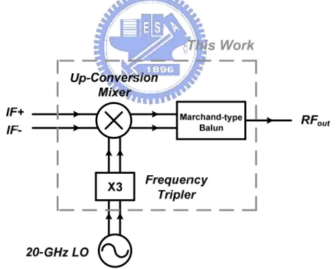
Based on the analysis done in Section 3.2, a 60-GHz direct up-conversion mixer is designed. Besides, an injection-locked frequency tripler is also integrated for providing LO signal. The up-converted RF differential signal is transformed to single-ended through a Marchand-type balun for the future integration with power amplifier (PA). Fig. 3.8 demonstrates the architecture of the whole fabricated circuits.
Fig. 3.8 Architecture of the fabricated circuits
3.3.1
Direct Up-Conversion Mixer
The proposed direct up-conversion mixer is shown in Fig. 3.9. M1/M2 is formed
a current source to provide a constant current for appropriate bias of M3 to M6. IF
signal is directly ac-coupled into the switching stage consisting of M3 to M6, instead
of a transconductor. This node is potentially to provide a slowly-varying impedance versus frequency, the return loss of IF port is therefore almost kept constant within a wide frequency band. The return loss at IF port is mainly determined by the bias current and the LO power. A larger bias current results in a lower impedance at IF port, and a larger LO power makes its impedance higher. This gives us a guideline to manipulate the matching at IF port.
Fig. 3.9 Schematic of the proposed up-conversion mixer
Fig. 3.10 is a simplified circuit which is used to choose the appropriate bias current for the up-conversion mixer. The conversion gain here is defined as:
. . | 20*log | i o IF freq v i RF freq magnitude of input voltage
CG
magnitude of output mixing current
→
⎛ ⎞
≡ ⎜⎜ ⎟⎟
⎝ ⎠ (3.2)
Fig. 3.10 Simplified circuit for choosing appropriate bias current
Fig. 3.11 demonstrates the normalized conversion gain versus bias current at different transistor sizes. Fig. 3.12 shows the corresponding VGS at the switching stage.
Fig. 3.11 gives us a guideline to choose the proper bias current. Fig. 3.12 shows the fact that the corresponding VGS of the optimum bias current at different transistor size
are the same. Furthermore, this VGS is at the location of maximum of Gm2, since the
first-order mixing is dominated by Gm2.
Fig. 3.11 Normalized conversion gain versus bias current
Fig. 3.12 The corresponding VGS at switching stage
24
The inductors at the drain of switching stage resonate out the parasitic capacitance for providing a high impedance at near 60 GHz for the mixing current. It is well-known that a Marchand balun could provide a broadband frequency response in the transformation between differential signal and single-ended signal. Furthermore, considering the future integration with PA, single-ended transformation is definitely essential. Altogether, Marchand balun seems to be a good choice to satisfy both the
requirements. Detailed description relating to Marchand balun would be in the Section 3.3.2.
Finally, the Lom in the Fig. 3.9 is a meandered transmission line which is used to
do output matching.
3.3.2
Marchand-type Balun
As mentioned in Section 3.3.1, Marchand balun is a good choice for satisfying the both requirements. According to the theory of the Marchand balun, four quarter wavelength transmission lines are utilized to do balance to unbalance transformation. In the other hand, at millimeter wave frequency, inductors are necessary for resonating out the parasitic capacitance of the active devices to peak the gain at the interested frequency. The equivalent inductance of the quarter wavelength transmission line is failed to meet the inductance that should be used for peaking the up-conversion mixer. Therefore, the first design priority was given to the inductance for shunt peaking, after this the balance to unbalance transformation is further considered.
Fig. 3.13 3-D view of Marchand-type balun
Fig. 3.13 shows the 3-D view of the Marchand-type balun [12]-[13], the metal in gray (Metal7) is the center-tapped inductor to peak the conversion gain of the mixer at 60GHz. The hook-shaped metal in black (Metal8) is stacked upon the center-tapped inductor, which acts just as a coupled line. The up-converted differential signal in the Metal7 is coupled to the Metal8 through both electrical and magnetic coupling. Iterative EM simulations were done to choose the optimal overlapped area between Metal7 and Metal8. This method accomplish the shunt peaking purpose and the balance to unbalance transformation, however, it fails to meet the basis of the Marchand balun. Thus, some extra insertion loss is introduced when performing the balance to unbalance transformation, as Fig. 3.14 indicates.
Fig. 3.14 Simulated gain difference before/after Marchand-type balun
3.3.3
Injection-locked Frequency Tripler
26
The function of the frequency pre-generator is implemented by MTri1 and MTri2.
The design guideline of MTri1 and MTri2 is the same as for the conventional frequency
multipliers in [11]. The conversion gain of the frequency pre-generator can be maximized with an appropriate gate bias of MTri1 and MTri2. The tripled-frequency
signal is injected into the injection-locked oscillator (ILO) formed by MTri3 and MTri4,
and LTri. The selected value of LTri is chosen so that the resonant frequency is close to
the third-order harmonic frequency of the input injection signal. MTri3 and MTri4 are
used to generate the negative resistance to compensate for the loss of the LC-tank. RD
is designed for the improvement of the harmonic rejection-ratios (HRRs). The ILFT has a current-reuse structure between the frequency pre-generator and ILO for low power operation. The detailed design and analysis of ILFT could be found in [15].
Fig. 3.15 Schematic of injection-locked frequency tripler
3.4 Experimental Results
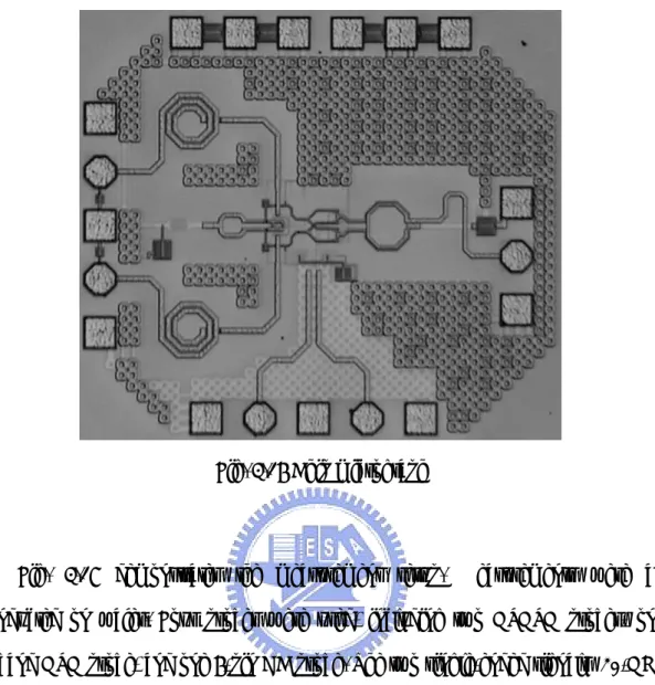
The circuits mentioned in Section 3.3, including a direct up-conversion mixer, Marchand-type balun, and an ILFT are designed and fabricated using TSMC 0.13-μm technology. The chip micrograph is shown in Fig. 3.16. Total chip area is 0.78 mm x 0.88 mm. The chip area is limited by the minimum distance between pads.
Fig. 3.16 Chip micrograph
Fig. 3.17 demonstrates the measurement setup. Measurements were all conducted on wafer. Four probes were used, including two GSGSG probes, one V-band GSG probe, and one 6-pin DC probe. The two single-ended signals (20-GHz LO and IF) from signal generators are transformed to differential through external baluns.
Fig. 3.17 Measurement setup
Following figures show the measured results of this work. The supply voltage is 1.2 Volt. Total power consumption, including mixer and tripler is 8.6 mW. The up-conversion mixer consumes 2.7 mW only.
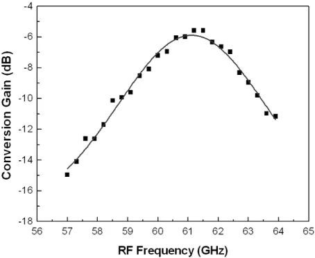
Fig. 3.18 shows the frequency response of the up-conversion mixer and frequency tripler as a whole. When measuring frequency response IF frequency was
fixed at 100 MHz, input of tripler was swept from57 GHz to 64 GHz
3 3 , and the
up-converted upper-sideband signal power is recorded, that is (57 GHz+100 MHz) to (64 GHz+100 MHz). The maximum conversion gain is -5.6 dB at 61.2 GHz. The bandwidth limitation can be due to the narrow-band response of the used ILFT. Fig. 3.19 demonstrates the normalized output swing of the ILFT.
Fig. 3.18 Measured frequency response of up-conversion mixer and frequency tripler
Fig. 3.19 Simulated frequency response of ILFT
Fig. 3.20 Measured output spectrum under -25 dBm IF input power
Fig. 3.21 Measured input 1-dB compression point of up-conversion mixer
Fig. 3.22 Measured input third-order intercept point of up-conversion mixer
Fig. 3.23 Measured output spectrum under -15dBm IF input power
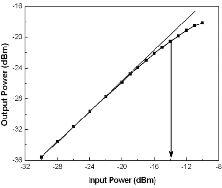
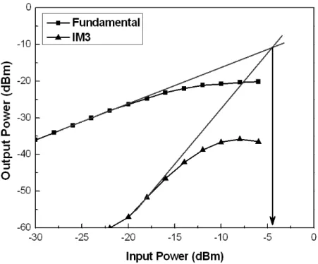
Both P-1dB and IIP3 were measured at the maximum conversion gain frequency
(61.2GHz). As Fig. 3.21 shows, the P-1dB of this up-conversion mixer is -14 dBm. IIP3
33
was measured with IF frequencies fixed to 90 MHz and 110 MHz, respectively. Due to the highest available frequency of the spectrum analyzer is lower than 60 GHz; RF signal was down-converted through an external V-band sub-harmonic mixer. This external mixer introduced a large loss, therefore the IM3 tones were below the noise floor when IF input power was lower than -22 dBm. The measured IIP3 is -4dBm as Fig. 3.22 indicates.
The measurement of IF bandwidth is rather cumbersome compared to other measurement items since there is no such a balun that covers a ultra-wide bandwidth (from several MHz to several GHz) with nice phase balance performance. Thus, several baluns were used to cover the interested bandwidth. The loss of each balun was calibrated before doing measurements. In addition, at the joint frequency of two band-successive baluns, the conversion gain using both two baluns were recorded and checked to guarantee the experimental accuracy when switching baluns. For example, the difference in measured conversion gain at 1GHz using balun A (500 MHz~1 GHz) and balun B (1 GHz~2 GHz) is below 1 dB. Fig. 3.24 demonstrates the measured IF bandwidth; 1-dB bandwidth is 2.5 GHz and 3-dB bandwidth is 3.5 GHz.
Fig. 3.24 Measured IF bandwidth of up-conversion mixer
The matching of IF port was measured to verify the slowly-varying idea. The measured impedances versus frequency from (50 MHz to 10 GHz) are shown in Fig. 3.25, in which the gray line demonstrates the stand-by condition (the tripler is off) and the black one shows the operation condition (the tripler is on with 0 dBm input power). The impedance is obviously to be slowly-varying within a wide bandwidth of 50MHz to 10 GHz. Fig. 3.26 shows the operation condition of IF port matching which corresponds to the black line shown in Fig. 3.25. In this figure, we can see more quantitatively that the return loss within 50 MHz to 10 GHz is kept at around 10 dB.
Fig. 3.25 Measured IF port matching
Fig. 3.26 Measured IF port matching at 0-dBm LO power
Fig. 3.27 Measured RF port matching at 0-dBm LO power
Fig. 3.27 shows the RF port matching measured at 0-dBm LO power, the return loss is below -10dB within 57GHz to 64GHz.
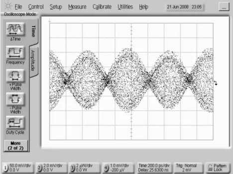
The time-domain waveform is also captured using a high-speed wideband oscilloscope. The measured output waveform with cables and probes losses, IF frequency of 1 GHz, and LO frequency of 61.2 GHz is shown in Fig. 3.28. It can be seen clearly, a quickly-varying signal is enveloped by a 1-GHz signal. This encircled high frequency signal cannot be observed clearly due to the operation principle of the sampling oscilloscope. A close-in waveform is shown in Fig. 3.29, in which a high frequency sinusoidal signal can be barely observed.
Fig. 3.28 Measured output waveform at IF frequency of 1GHz and LO frequency of 61.2GHz
Fig. 3.29 Measured output waveform at IF frequency of 1GHz and LO frequency of 61.2GHz (close-in)
38
Ref. This work
(measured) [13] [14]
Technology 0.13-μm CMOS 90-nm CMOS 0.13-μm CMOS
Frequency Range 58.3GHz ~ 62.5GHz 50GHz 22GHz ~ 29GHz Conversion Gain -5.6dB ~ -8.6dB -11dB -2dB ~ 0.7dB IF Bandwidth 1dB : 2.5GHz 3dB : 3.5GHz N/A 3dB : 1.8GHz IP1dB -14dBm 1dBm -5dBm Power Consumption 2.7mW 13.5mW 9.6mW
Table 3.1 Comparison with published up-conversion mixers
3.5 Summary
A direct up-conversion mixer with wide IF bandwidth is designed and fabricated for 60-GHz applications. Large-signal has been verified to estimate the accurate trend of impedance versus frequency at IF port. According to the experimental results, the up-conversion mixer has 3.5-GHz IF bandwidth which is feasible for high-speed data transmission.
39
Chapter 4
Frequency Tripler Using Second-Order Harmonic
Current Injection Technique
4.1 Introduction
Active frequency multipliers are utilized in numerous applications to efficiently provide a source of high frequency microwave energy. They are commonly used in communication systems to enable frequency translation of a signal from a low-noise low-frequency oscillator to the required higher frequency band for the purpose of up/down conversion in transceivers.
In general, frequency triplers and higher order multipliers have not seen prominence and detailed investigation benefited by doublers, due to higher circuit complexity and lower achievable conversion gain and efficiency [7]-[10], [16]-[17].
Driving the transistors into strongly non-linear region to obtain the square wave then filtering out the desired harmonic as existing frequency triplers do has the disadvantage of low conversion efficiency. Since most power are wasted in the undesired frequency components. Due to its poor conversion efficiency, designers usually have to boost the third harmonic in the following stage which results in more power consumption.
In this work, a novel technique of generating the third-order harmonic is proposed and analyzed. Applying this technique, third-order harmonic can be generated under low power consumption and the circuit itself is uncomplicated compared with other published methods. Furthermore, the proposed technique is especially suitable for the communication systems that utilize I/Q signals for image rejection. Analytical
40
equations were developed to approximate the numerically-converged results of CAD tools for optimization with paper and hand calculation. Detailed analyses were done to maximize the third-order harmonic and suppress the undesired harmonics. According to the simulation results, the proposed harmonic current injection frequency tripler (HCI-FT) has -5.6 dB conversion gain under only 2.6 mW dynamic power consumption with fundamental input power of +2 dBm. The proposed HCI-FT is fabricated using 0.18-μm standard CMOS technology for the verification of theoretical results.
In Section 4.2 the analyses relating to the second-order current injection is investigated. The design considerations are mentioned in Section 4.3. The chip implementation and simulation results are presented in Section 4.4. Finally, a summary is given in Section 4.5.
4.2 Second-Order Current Injection
The proposed harmonic current injection frequency tripler (HCI-FT) was developed from the concept shown in Fig. 4.1. We try to generate third-order harmonic using mixers. The easiest way to accomplish our purpose is using two Gilbert cell mixers in cascade, as Fig. 4.2 shows.
Fig. 4.1 Block diagram of generating third-order harmonic
Fig. 4.2 The straightforward implementation of our idea
41
The first mixer is used to generate the second-order harmonic for feeding the second mixer. In RF communication circuit design, we are all familiar with Gilbert cell mixer, and it is not difficult to design, however, it seems inefficient to generate the second-order harmonic in this way. There is still some other more efficient and easier ways for generating this desired harmonic, Fig. 4.3 is an example. At the joint of a source-coupled pair, there is an inherent second-order harmonic if the
fundamental signal was applied at the gate terminal. Thus, a simplified and more efficient circuit of implementing the function of the block diagram above is as Fig. 4.4 demonstrates.
Fig. 4.3 A source-coupled pair
Fig. 4.4 Simplified circuit
The second-order harmonic is generated by the source-coupled pair and it propagates to the transconductance stage of the mixer. After current commutating at switching stage, both fundamental and the third-order are generated. Nonetheless, we
still strive to simplify this circuit, since it takes three steps to generate the final second-order current for commutating as Fig. 4.4 marks.
Fig. 4.5(a) is the fully-simplified circuit we finally come out with. The second-order harmonic generation part is directly folded to the bottom of switching stage in a cascode configuration. Not only it simplifies the circuit complexity, the current-reuse structure also makes it advantageous in low-power circuit implementation. V(fo) V(fo) I(2fo) V(fo) V(fo) V(fo) , V(3fo) (a) (b)
Fig. 4.5 (a) Fully-simplified circuit and its (b) conceptual circuit
Fig. 4.5(b) shows the conceptual circuit of the fully-simplified circuit. The second-order current is generated by the bottom differential pair, and this current is injected into the upper differential pair. The fundamental input signal at the gate of the upper differential pair makes current commutation; it works as the mixing stage of a conventional mixer. Therefore, the mixing frequency, fo and 3fo are generated at
output.
4.2.1
Output Current versus Injection Phase
To evaluate the feasibility of the fully-simplified circuit in Fig. 4.5(a), we have to identify its mechanism first. For the convenience of analyzing this circuit, we substitute the second-order harmonic generation part into an ideal current sink which draws a DC current and injects an AC current (the second-order current) at the same time, as Fig. 4.6 indicates.
f0 f0 Ibias + Iinj MU2 DC AC MU1 X
Fig. 4.6 Further simplified for analyzing
A third-order harmonic current is expected at the output (drain terminal) as this second-order current is injected. Let the second-order injection current expresses as:
Iinj=|Iinj|∠Iinj (4.1)
where |Iinj| is the injection magnitude, and ∠Iinj is the injection phase.
It is intuitively that the larger injection magnitude would results in larger output third-order current. However, the larger injection magnitude implies the larger fundamental input power is needed. This is definitely not the way for low-power design. So, we are interested in the injection phase. We want to know what happened to the output current under various injection phase.
(a)
(b)
(c)
45
Therefore, in the preliminary investigations, injection magnitude is fixed and output current under various injection phase is observed. Fig. 4.7 shows the results. The fundamental, the second-order harmonic and the third-order harmonic current are observed at the output. They are normalized to the corresponding harmonic current magnitudes without injection and shown in dB scale, respectively.
From Fig. 4.7(c), the third-order output current at 0º injection phase is 2.7 dB more than that without injection, and is near 7dB more than that of 180º injection phase. Moreover, at 0º injection phase, the undesired fundamental current has its minimum. If we define the harmonic rejection ratio (HRR) as:
HRRn = 20 log Desired harmonic
Undesired n-th order harmonic ⎛
× ⎜
⎝ ⎠
⎞
⎟ (4.2) In our case, the desired harmonic is the third-order harmonic, and the undesired harmonics are fundamental and the second-order harmonic.
Not only the third-order harmonic current is maximized at 0º injection phase, fundamental current is also minimized at this injection phase, thus the best HRR1. If
an improper injection phase was chosen, say ∠Iinj =180º, it would lead to the worst
results, in which the third-order harmonic current is minimized and fundamental current is maximized. From the above investigation, the 0º injection phase is the optimal injection phase.
It will be more easily to know what happened to the third-order output current if we partition the circuit shown in Fig. 4.6 into a DC current part (without current injection) and a AC current part (with current injection) as Fig. 4.8 depicts. The part without current injection is simply a differential pair biased by a constant DC current. As we all know, the transistors of an ideal differential pair draw the bias current alternatively as two switches. Therefore, there is a square-wave-shaped current at its output, which contains the third-order harmonic component. In a word, there exists a
third-order harmonic current at the output of “Part A” shown in Fig. 4.8 even without current injection. Things will be much clearer if the output current is shown in a complex plane, which enable us to observe magnitude and phase simultaneously. Fig. 4.9(a) demonstrates the overall third-order output current and the third-order output current without current injection. It is evident that the phase of the overall third-order current at ∠Iinj =0º (which we choose to be the optimal injection phase above) is
in-phase with the phase that without current injection.
f0 f0 Ibias + Iinj MU2 DC AC MU1 X f0 f0 Ibias MU2 MU1 X Iout,w/o injection f0 f0 Iinj MU2 MU1 X Iout, injected Part A Part B Iout,overall
Fig. 4.8 Conceptual circuit partition
(a) (b)
Fig. 4.9 Normalized (a) overall output third-order current and output third-order current without current injection (b) injected contribution in complex plane
The overall third-order output current (Iout, overall) is the linear combination of that
without injection (Iout, w/o injection) and that with injection (Iout, injected). Moreover, it is
reasonable to assume that under some injection level, the phase of the third-order output current without current injection is unchanged. Then, the contribution of the injected current can be defined as:
, , , /
out injected out overall out w o injection
I =I −I (4.3)
Fig. 4.8(b) shows the contribution of the injected current. We can conclude that if ∠Iinj =0º, then ∠Iout, injected = ∠Iout, w/o injection, therefore the |Iout, overall| is maximized.
4.2.2
Injection Node
So far, the output current what we most concern with is analyzed. However, we also wanna know what happened to the injection node X in Fig. 4.6.
A source-coupled pair is inherently to generate a second-order harmonic signal at
the joint as Fig. 4.3 shows. Let the VmRef be the reference voltage without
second-order injection current. It is reasonable that under some injection level, VmRef
is supposedly unchanged or its variation is negligible.
f0 f0 Ibias + Iinj MU2 MU1 Vm 2f0
Fig. 4.10 Source-coupled pair with second-order current injection
Re Im VmRef
V
m(2ω
o)
Vm Injected Contribution Re Im VmRefV
m(2ω
o)
(a) (b)Fig. 4.11 second-order harmonic voltage of Vm (a) without (b) with second-order
current injection
Fig. 4.11 shows the second-order harmonic voltage of Vm in complex plane. As
mentioned above, under some injection level VmRef is unchanged, thus the resulting
voltage Vm’ with second-order current injection is the linear combination of vector
VmRef and the vector injected contribution. This is like what we do in Section 4.2.1,
which partitions the overall result into an intrinsic part and an extrinsic part.
Fig. 4.12 Normalized third-order output current under different injection level
Fig. 4.12 demonstrates the magnitude of the third-order output current under various injection level with normalized to the non-injection condition in dB scale. Still, the optimal injection phase is 0º.
Coincidentally, the 0º injection phase results in the maxima of the second-order voltage (Vm’) at the injection node at the same time, and these maxima are in-phase
with VmRef. Fig. 4.13 shows the detail in complex plane. The dot which locates on
the unit circle is the VmRef, and the injection phases which result in the maxima
third-order output current at different injection level are marked with crosses.
50
with VmRef, a maximum third-order current is obtained at the output.
The injected contribution here is in voltage-domain, however, our input (injection current) is in current-domain. The relationship between them should be explained. Since the node Vm is a low impedance node, the first pole of this node may
be far from the frequency of the second-order harmonic if the fundamental frequency is not too high. Therefore, the voltage contributed by the injection current at this node is almost in-phase with the injection current. In fact, the resulting voltage of the injection current has a little negative phase shift since the parasitic capacitances make this node capacitive.
Fig. 4.13 Normalized third-order output current under different injection level in complex plane