國 立 交 通 大 學
電信工程學系
碩 士 論 文
高差動輸入訊號及共模電壓範圍之五階轉
導電容濾波電路
A Fifth-Order gm-C Filter with Large
Differential Input Signals and Wide
Common-Mode Voltage Ranges
研 究 生:李三益
指導教授:洪崇智 教授
高差動輸入訊號及共模電壓範圍之五階轉
導電容濾波電路
A Fifth-Order gm-C Filter with Large
Differential Input Signals and Wide
Common-Mode Voltage Ranges
研 究 生:李 三 益
Student:San-Yi Lee
指導教授:洪 崇 智 教授
Advisor:Prof. Chung-Chih Hung
國立交通大學
電信工程學系 電信研究所碩士班
碩 士 論 文
A Thesis
Submitted to Department of Communication Engineering College of Electrical Engineering and Computer Science
National Chiao-Tung University In Partial Fulfillment of the Requirements
For the Degree of Master of Science
In
Communication Engineering January 2006
Hsinchu, Taiwan, Republic of China
中華民國九十五年一月
高差動輸入訊號及共模電壓範圍之五階轉
導電容濾波電路
學生:李三益 指導教授:洪崇智 教授
國立交通大學
電子工程學系 電信研究所碩士班
摘要
本篇論文設計了一具有高差動輸入訊號及高共模輸入電壓範圍的五階低通 gm-C濾波器。在設計出此一濾波器之前,我們必須先設計出一具有低電壓高差動 輸入訊號及高共模輸入電壓範圍的轉導放大器(電壓-電流轉換器)。此轉導放 大器是由一N型的轉導放大器電路並聯一P型的轉導放大器組合而成。並且此兩 個轉導放大器在輸出端分別連接一電流鏡,以求達到一個具有高差動輸入訊號及 高共模輸入電壓範圍的電路。對gm-C濾波器而言,其有一使用調整電路來補償製 程與溫度變化的必要性。而在本篇論文中我們必須使用到兩個調整電路來分別對 N型轉導放大器以及P型轉導放大器來做電路的控制電壓調整動作,以求此濾波 器能有一固定及穩定的截止頻率,並且維持N型轉導放大器與P型轉導放大器之 間轉導值的相等。此濾波器是操作在1.8V的供應電壓下,截止頻率可調範圍為 1.6MHz至2.4MHz之間,功率消耗為0.75mW,並且具有±0.7V的高差動輸入訊號及 高共模輸入電壓範圍。A Fifth-Order gm-C Filter with Large Differential Input
Signals and Wide Common-Mode Voltage Ranges
Student:San-Yi Lee Advisor:Prof. Chung-Chih Hung
Department of Communication Engineering
National Chiao-Tung University
Abstract
This thesis presents a low-voltage CMOS fifth-order elliptic low-pass gm-C filter with large differential input swings and wide common-mode ranges. The Operational Transconductance Amplifier (OTA) is a low-voltage CMOS voltage-to-current (V-I) converter. The basic OTA cell with NMOS-inputs is connected in parallel with its counterpart PMOS-input OTA circuit, in conjunction with NMOS and PMOS output current mirrors, to achieve large input signal and common-mode voltage ranges. For the gm-C filter, additional tuning circuitry is required in order to compensate the process and temperature variation.. In this OTA design, two frequency tuning circuits are utilized, respectively, to adjust the control voltage of NMOS-input and PMOS-input OTAs so as to fix the filter cutoff frequency and also maintain the equivalence between the two transconductance of NMOS-input and PMOS-input OTAs. The gm-C filter operates with supply voltage of 1.8V, has cutoff frequency of 1.6MHz to 2.4MHz, dissipates 0.75mW power, and has large differential input signals and wide common-mode voltage ranges of ±0.7V.
Ackonwledgement
First, I would like to express my immense gratitude to my adviser Dr. Chung-Chih Hung, for his enthusiastic and patience guidance throughout this research work. I am deeply indebted to him for all the knowledge and help which he has extended to me.
Second, I would also like to thank my all team members of the AIC group: Tien-Yu Lo, Chih-Lun Chuang, Chia-Wei Chang, Chun-Hung Chiu, and Chun-Yueh Yang . They have helped me to enhance my knowledge through various discussions and interactions. Special mention goes to Ming-Dou Ker and Materials Analysis Technology Inc. They also gave me many supports to my research work.
Finally, I would like to thank my family. My parents give me the most supports and care in all my life and for that I am forever grateful. My sister, brother and my girlfriend have always providing me timely encouragement and suggestion. To all the people who have helped me in my life, I would like to say “thank you”.
國立交通大學
Table of contents
Abstract(Chinese)………I
Abstract(English)……….II
Acknowledgement………III
Table of Contents………...IV
List of Figures……….VI
List of Tables………VIII
Chapter I Introduction……….1
1.1 Overview of integrated analog filters……….1
1.2 Motivation……….……….3
Chapter II Design of Operational Transconductance Amplifier...…4
2.1 Linear Tunable OTA…………..……….4
2.2 Modified Linear Tunable OTA……….6
2.2.1 CMOS Composite Transistors……….6
2.2.2 Modified Tunable OTA………..8
2.3 An equivalent Single-ended Input OTA with Large Differential Input Signal and Wide Common-Mode Voltage Ranges………9
2.4 An Equivalent Differential-Input OTA with Large Differential Input Signals and Common-Mode Ranges……….15
2.5 Simulation Results………17
Chapter III Design of Tuning Circuit………...19
3.1.2 General Concepts in Tuning………20
3.2 Introduction of Practicable Tuning Circuits……….21
3.3 Implementation of the Tuning Circuit………26
3.4 Simulation Results of the Tuning Circuit……….29
Chapter IV Design of Continuous-Time Gm-C Filters………31
4.1 Fundamental Concepts of Analog Filters……….31
4.2 LC Ladder Simulation by Signal-Flow Graphs………32
4.2.1 Introduction of LC Ladder Filters………...32
4.2.2 LC Ladder Simulation by Signal-Flow Graphs………...33
4.3 Fifth-Order Elliptic Low-Pass GM-C Filter……….42
4.4 Total Harmonic Distortion (THD)………45
4.5 Simulation Results of the Filter………47
Chapter V Post Layout Simulation Results………49
5.1 Post Layout Simulation Results of the OTA……….………49
5.2 Post Layout Simulation Results of the gm-C filter………51
Chapter VI Conclusions and future research……….55
List of Figures
Figure 1.1 Direct-conversion WCDMA receiver system……….3
Figure 2.1 Basic cell of linear transconductor………4
Figure 2.2 (a) a single transistor (b) a CMOS composite transistors……….7
Figure 2.3 Modified linear transconductor and its symbol N-gm………9
Figure 2.4 V-I curve of the basic V-I converter circuit with V2=0V………10
Figure 2.5 Circuit diagram of the N-OTA composed by the basic N-type V-I converter and an NMOS current mirror……….10
Figure 2.6 V-I curve of the transistor MN9 of the N-OTA circuit………11
Figure 2.7 the circuit of the basic P-gm cell……….12
Figure 2.8 Circuit diagram of the P-OTA composed by the basic P-type V-I converter and a PMOS current mirror………12
Figure 2.9 V-I curve of the transistor MP9 of the P-OTA circuit………13
Figure 2.10 Equivalent single-ended OTA composed by the parallel connection of N-OTA and P-OTA………..14
Figure 2.11 V-I curve of the single-ended OTA………...14
Figure 2.12 Differential-input OTA architecture………16
Figure 2.13 differential-input OTA’s symbol………...17
Figure 2.14 V-I curve of the differential-input OTA with V2 = 0V……….17
Figure 2.15 V-I curve of the differential-input OTA with V1 = 0V……….18
Figure 2.16 The linearity error of Gm value at different input common-mode Voltages………18
Figure 3.1 Indirect frequency tuning architecture………20
Figure 3.3 Constant transconductance tuning circuit with current controlled……….22
Figure 3.4 frequency tuning circuit……….23
Figure 3.5 A frequency tuning circuit that operate at a lower clock frequency……...24
Figure 3.6 Frequency tuning circuit using a phase-locked loop………...25
Figure 3.7 N-type frequency tuning circuit………..28
Figure 3.8 P-type frequency tuning circuit………28
Figure 3.9 The entire architecture of the frequency tuning circuitry………...29
Figure 3.10 Transient response of the output control voltage, Vnctrl………29
Figure 3.11 Transient response of the output control voltage, Vpctrl………30
Figure 4.1 Resistively terminated lossless twoport………..32
Figure 4.2 Resistively terminated ladder structure………...33
Figure 4.3 Section of a ladder network………34
Figure 4.4 Signal-flow graph block diagram representation of the ladder section in Figure 4.3………...36
Figure 4.5 Transformation resulting in only positive input summers………..37
Figure 4.6 The diagram of Figure 4.5 redrawn in the leapfrog (LF) configuration….37 Figure 4.7 Fourth-order lowpass ladder………38
Figure 4.8 Simulation flow diagram of the ladder of Figure 4.7………..39
Figure 4.9 (a) Inverting lossy Miller integrator; (b) noninverting lossy phase-lead Integrator………39
Figure 4.10 Active realization of the LC ladder of Figure 4.7……….40
Figure 4.11 Fifth-order elliptic LC lowpass filter………42
Figure 4.12 Typical ladder section with a floating capacitor………...43
Figure 4.13 Realizations of Equations (4.23) and (4.24)……….44
Figure 4.14 Gm-C SFG simulation of the circuit in Figure 4.11……….45 Figure 4.15 The frequency responses of the gm-C filter with the common-mode
voltage at 0V, -0.6V, and 0.6V………47 Figure 4.16 Tunable range of the cutoff frequency. 48 Figure 4.17 Total harmonic distortion of the filter for different input voltages……...48 Figure 5.1 Post layout: DC response of the OTA with different corner
(a)tt (b)ss (c) ff at V1=0v………50 Figure 5.2 Post layout: DC response of the OTA with different corner
(a)tt (b)ss (c) ff at V2=0v………51 Figure 5.3 Post layout: frequency responses of the gm-C filter with the
common-mode voltage at 0V, -0.6V, and 0.6V………51 Figure 5.4 Post layout: transient response of gm-C filter with 1MHz input signal….52 Figure 5.5 Post layout: transient response of gm-C filter with 2MHz input signal….52 Figure 5.6 FFT analysis of the filter output………..53 Figure 5.7 The layout of the gm-C filter………..54
List of Tables
Table 1.1 Comparisons with other references………2 Table 5.1 The specifications of the fifth-order elliptic low-pass gm-C filter………53
Chapter I
Introduction
1.1 Overview of integrated analog filters
In the natural world, the quality of the signal might be influenced by noise. Hence, in order to remove the disturbance of noise, we must develop filters. In 1915, the basic concepts of the electric filter were developed independently by Wagner in Germany and Campbell in the United States. Up to now, filter theory and implementation techniques have been developed to a high degree of perfection. There are two main techniques for realizing integrated analog filters. One technique is the use of switched-capacitor circuits. The second popular technique for realizing integrated analog filters is the continuous-time filter. A switched-capacitor circuit, although its signal remains continuous in voltage, is, in fact, a discrete-time filter since it requires sampling in the time domain. Typically the clock rate is much greater than twice the signal bandwidth, to reduce the requirements of an anti-aliasing filter. As a result, switched-capacitor filters are limited in their ability to process high-frequency signals. Oppositely, continuous-time filters have a significant speed advantage because no sampling is required.
Continuous-time filters can operate successfully on high-speed signals, but they still have some disadvantages. One disadvantage is the requirement of the tuning circuitry. Although switched-capacitor filters have coefficient accuracies of 0.1 percent, Continuous-time filters’ coefficients are initially set to only about 30% accuracy. Since, without a tuning mechanism, the performance of continuous-time
filters will vary terribly due to process and temperature variation. Another practical disadvantage is their relatively poor linearity and noise performance. Fortunately, there are some high-speed applications in which distortion and noise performances are not too demanding, such as many data communication and video circuits. Hence continuous-time filters have been used extensively in many spheres, and more and more researches of continuous-time filter, e.g. high frequency, high dynamic range[1,2,3,4,5,6,7,10,11,12], wide common voltage ranges or low distortion etc., have been published. In this thesis, we will aim at large input signals and wide common-mode voltage ranges. Table 1.1 shows the comparisons with other references. This fifth order elliptic low-pass GM-C filter operates at a supply voltage of 1.8V and has a cutoff frequency of 1.6 to 2.4 MHz. It provides up to 1.4Vpp output with 1% total harmonic distortion (THD), dissipates 0.75mW, and occupies 1.07mm2 in 0.18-um CMOS technology.
References [7] [8] [9] This work
Technology 0.8-umCMOS 0.35-umCMOS 0.25umCMOS 0.18umUMC
Supply voltage 3V 2.5V 2.5V 1.8V -3dB frequency 4MHz 1MHz 1.1MHz 1.6MHz~2.4MHz Input signal range 0.625mV 1V 1V 1.4V Automatic
tuning Yes Yes Yes Yes
THD -40dB -54dB -85dB -40dB
Power
consumption 10mW 11.25mW 16mW 0.75mW
1.2 Motivation
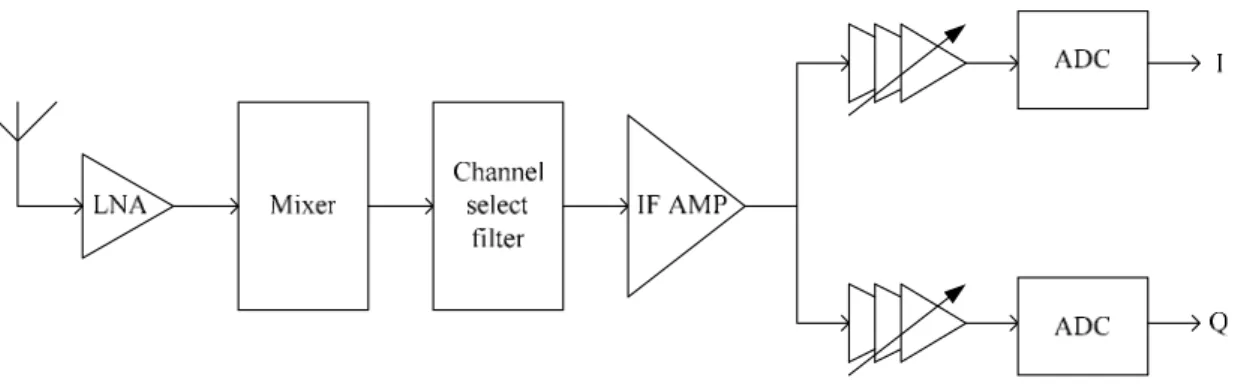
With the development of the third-generation (3G) wideband code-division multiple-access (WCDMA) wireless cellular networks, the need for low-cost, low power consumption, and high integration is becoming important for the commercial development of 3G mobile handsets. A direct-conversion receiver IC was designed for the WCDMA mobile systems. By using the WCDMA systems, the speed of the transmission of data would be promoted substantially. The direct-conversion receiver architecture with the proper use of silicon process, circuit design techniques and architecture implementation represents a promising system solution for high
integration platforms for 3G handsets. Figure 1.1 shows the architecture of the WCDAM direct-conversion receiver system[14,15], and we will put emphasis on the channel select filter in the thesis. In past days, the channel select filter wasn’t included in the entire chip, but now, in a IF receiver IC, channel selectivity is achieved at baseband by on-chip low-pass filters. In order to achieve the integration of the system-on-chip(SOC), the development of the active filter have become the key point of the research.
Chapter II
Design of Operational
Transconductance Amplifier(OTA)
In this thesis, the design of a low-voltage CMOS fifth-order elliptic low-pass Gm-C filter with large differential input swings and wide common-mode ranges is presented. This filter consists of seven identical differential-input operational transconductance amplifiers (OTAs) and seven capacitors, and we will introduce the design of the OTA circuits with large differential input swings and wide common-mode ranges in this chapter.
2.1 Linear Tunable OTA
composite n-channel MOSFET[6] which is composed of matched transistors M1, M2 and M3. Figure 2.1 shows a basic cell of the linear OTA. The currents I1, I2, I3, and I4
can be expressed as 2 1 1 ( 1 2 2 n ss tn K V V ) I = V − + −V (2.1) 2 2 2 ( 2 2 n ss c tn K V V ) I = + − −V V (2.2) 2 1 3 ( 2 2 n ss c tn K V V ) I = + − −V V (2.3) 2 2 4 ( 2 2 2 n ss tn K V V ) I = V − + −V (2.4)
where all the transistors are operating in the saturation region, Kn =(µ εn / )(tox W1/L1), and Vt is the threshold voltage.
The transistor sizes of M1-M6 are all matched and equal to W1/L1, so the transconductance parameters of M1-M6 are all the same, too. The gate voltage of M2 is equal to (V1+Vss)/2 because the transistor size of M1 is the same to M3 and the
source of each transistor is connected to the bulk. The differential output current of the basic transconductance cell is given by
1 2 ( 3 4
a b
I − = + −I I I I +I ) (2.5) By substituting equations (2.1), (2.2), (2.3), and (2.4) into (2.5), we can obtain
1 2 ( )( 2 n a b c ss K I − =I V −V V − )V (2.6) This linear OTA has a constant Gm given by Gm = Kn(Vc-Vss)/2, which can be tuned by Vc. One disadvantage of this OTA circuit is that the linear input range is limited by
ss tn 1,2 dd tn 1,2 V + 2V V V + V V 2(Vc V ) Vtn ss ≤ ≤ ⎧⎪ ⎨ ≥ + − ⎪⎩ (2.7)
With the reduction of the power supply voltage, the input range and common-mode voltage ranges will be also decreased. Another disadvantage is that the control voltage is connected in the source terminal of the transistors M2 and M5, so that the control voltage is hard to control.
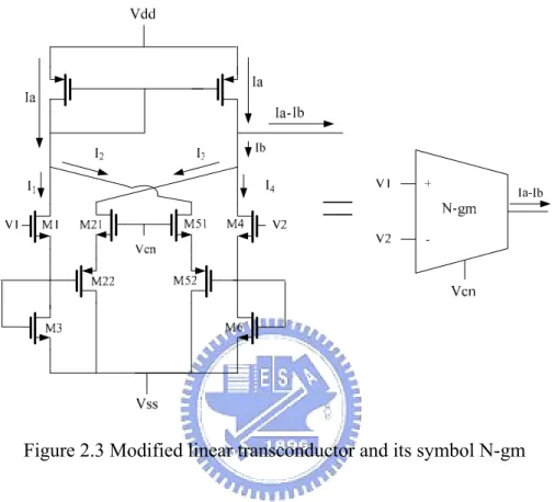
2.2 Modified Linear Tunable OTA
In order to increase the linear input range and change the connection of control voltage from source to gate terminal at the same time, the basic OTA circuit is modified by replacing transistors M2 and M5 with CMOS composite transistors[19] as shown in Figure 2.3.
2.2.1 CMOS Composite Transistors
Figure 2.2 shows a single transistors and a CMOS pair consisting of an n-channel and a p-channel transistors. For each NMOS transistor, we have
2 GS tn I = (V -V ) 2 K (2.8)
so we can obtain the gate-to-source voltage in the form
GS
2
V =Vtn I
K
+ (2.9)
For the CMOS composite transistors, the gate-to-source voltage of the transistors, Mn and Mp, can be expressed as:
GSn 2 V =Vtn n I K + (2.10) GSp 2 V =Vtp p I K − (2.11)
We can define an equivalent gate-to-source voltage , which can,
with the aid of (2.9), (2.10), and (2.11), be expressed as follows:
GSeq GSn SGp V = V + V GSeq GSn SGp tn tp n p 2I 2I V = V + V = V - V + + K K (2.12)
Equation (2.12) can be written in the same form as (2.9):
GSeq teq
eq 2I V = V +
K
where the equivalent parameters are given by
(2.14) (2.13) teq tn tp V = V - V eq n p 1 1 = + K K 1 K (2.15) (a) (b) Figure 2.2 (a) a single transistor (b) a CMOS composite transistors
Thus it is istor and
.2.2 Modified
Tunable
OTA
In Figure 2.3, the basic circuit of linear transconductor is modified by replacing tran
shown that a CMOS composite transistors acts as a single trans
with equivalent threshold voltage and transconductance parameter given by equation (2.14) and (2.15).
2
sistors M2 and M5 with CMOS composite transistors M21, M22, M51 and M52[6], where the equivalent transconductance parameter and threshold voltage are given by equation (2.14) and (2.15), respectively. By using the same way to the basic cell of linear transconductor, the currents I1, I2, I3, and I4 can be expressed as
2 1 1 ( 1 ) 2 2 n ss tn K V V I = V − + −V (2.16) 2 2 2 2 ( 2 ) eq ss cn teq K V V I = V − + −V (2.17) 2 1 3 ( ) 2 2 eq ss cn teq K V V I = V − + −V (2.18) 2 2 4 ( 2 ) 2 2 n ss tn K V V I = V − + −V (2.19)
If we choose W/L of the PMOS transistors M22 & M52 to be much larger than that of the NMOS transistors M21 & M51, the equivalent transconductance parameter Keq
will be very close to Kn and then we can obtain
1 2 ( ) 2 n a b cn ss tn teq K ( ) I − =I V −V −V −V V −V (2.20)
ss tn 1,2 dd tn 1,2 V + 2V V V + V V 2(Vc V ) Vteq ss ≤ ≤ ⎧⎪ ⎨ ≤ − − ⎪⎩ (2.21)
which is much better than equation (2.7).
Figure 2.3 Modified linear transconductor and its symbol N-gm
2.3 An equivalent Single-ended Input OTA with Large Differential
Input Signal and Wide Common-Mode Voltage Ranges
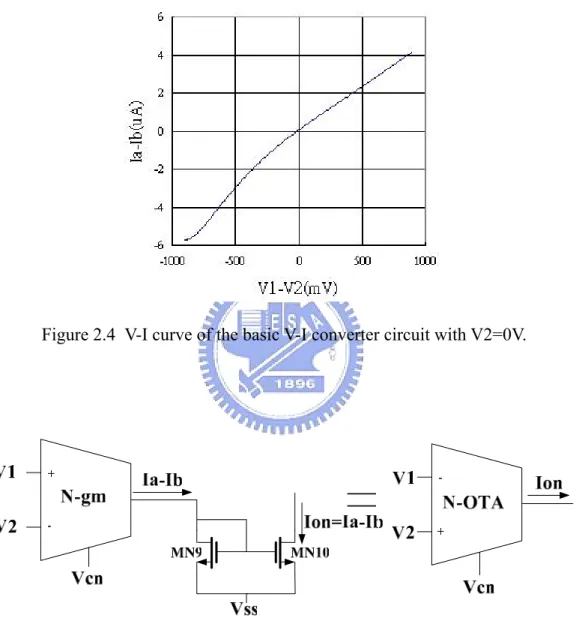
Although we have modified the linear transconductor to increase the linear input range, the input signal and common-mode voltage ranges are still too low. The NMOS input transistors in Figure 2.3 can only be maintained in the saturation region when the input common-mode voltage is larger than Vss+2Vtn. Figure 2.4 shows the V-I
curve of the basic V-I converter circuit. The linearity of the V-I curve could not be maintained when the input voltage V1 is too low.
Figure 2.5, to cancel the left-half plane of the V-I curve shown in Figure 2.4. Figure 2.6 shows the V-I curve of the N-OTA circuit, and the current flows into the transistor MN9 will become zero when V1<V2.
Figure 2.4 V-I curve of the basic V-I converter circuit with V2=0V.
Figure 2.5 Circuit diagram of the N-OTA composed by the basic N-type V-I converter and an NMOS current mirror.
Figure 2.6 V-I curve of the transistor MN9 of the N-OTA circuit
The V-I equation of the new N-OTA can then be expressed as:
1 2 1 1 2 ( )( ) 2 0 n on cn ss Tn Teq K 2 I V V V V V V when V V when V V = − − − − − > = ≤ (2.22)
When V1>V2, the output current flows into the N-OTA. When V1≤V2, the output current becomes zero.
In addition to the N-OTA, with which we have to use a complementary circuit P-OTA to combine, so that we can obtain a highly linear and high input voltage range converter. In order to design the complementary circuit P-OTA, we must design a basic P-gm cell first. Figure 2.7 shows the circuit of the basic P-gm cell, and the V/I equation can be expressed as follow:
1 2 ( ) 2 p d c cp dd Tp Teq K ( ) I − = −I V −V −V +V V −V (2.23)
Figure 2.7 the circuit of the basic P-gm cell.
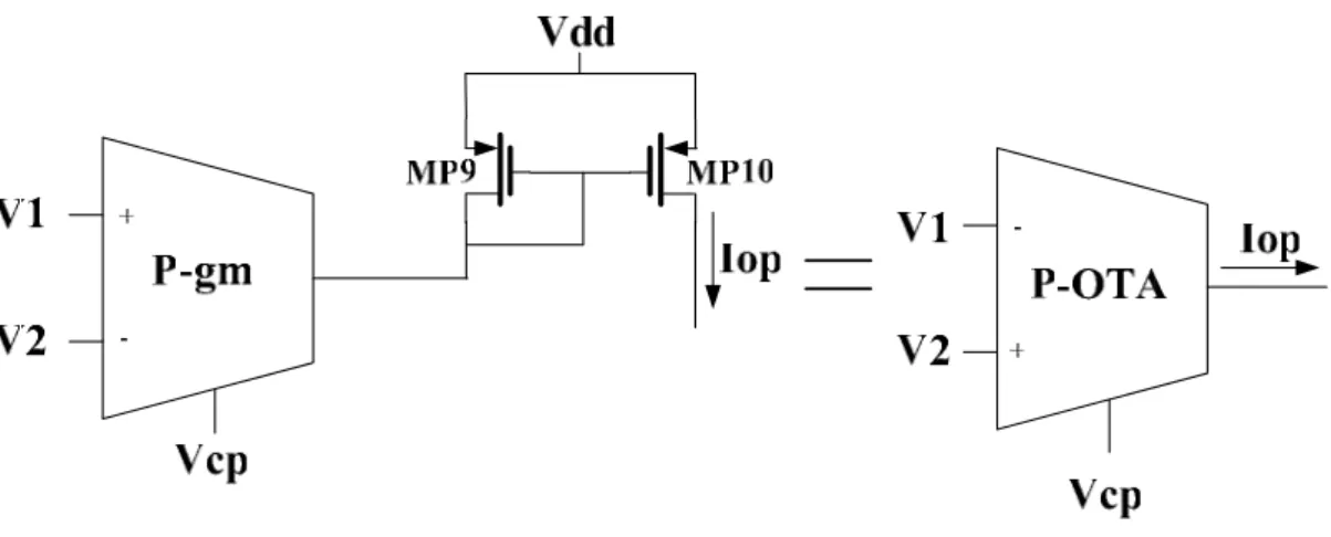
The circuit diagram of the P-OTA is presented in Figure 2.8. For the same reason, the P-gm cell and a PMOS current mirror link together. Figure 2.9 shows the V-I curve of the P-OTA circuit, and the current flows into the transistor MP9 will become zero when V1>V2.
Figure 2.8 Circuit diagram of the P-OTA composed by the basic P-type V-I converter and a PMOS current mirror.
The voltage-to-current relationship of the P-OTA is shown in Equation (2.24). 1 2 1 2 1 2 ( )( ) 2 0 p op cp dd Tp Teq K I V V V V V V when V V when V V = − − + − < = ≥ (2.24)
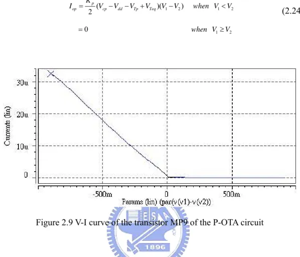
Figure 2.9 V-I curve of the transistor MP9 of the P-OTA circuit
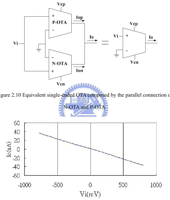
Combine the complementary circuit P-OTA with the N-OTA, we can obtain a V-I converter with large input signal and wide common-mode voltage ranges. Figure 2.5 shows that an N-OTA cell and its complementary P-OTA cell are connected in parallel. According to Equations (2.22) and (2.24), the output current is always negative when V1>V2 and always positive when V1<V2. Therefore, the parallel connection of N-OTA and P-OTA cells works like an equivalent single-ended OTA, as illustrated in Figure 2.5, by grounding the positive input terminal and setting the negative input terminal to be Vi=V1-V2. The output current Io of the equivalent OTA can be simplified as ( ) 2 ( ) 2 n o on cn ss Tn Teq i p op cp dd Tp Teq i K I I V V V V V when Vi K I V V V V V when Vi = = − − − − ≥ = = − − + ≤ 0 0 (2.25)
The V-I curve of the single-ended OTA is shown in Figure 2.11. The left-half plane (the positive current) of the V-I curve is the current flowing out of P-OTA and the right-half plane (the negative current) of the V-I curve is the current flowing into N-OTA.
Figure 2.10 Equivalent single-ended OTA composed by the parallel connection of N-OTA and P-OTA
Figure 2.11 V-I curve of the single-ended OTA.
It can be seen from Equation (2.25) that in order to ensure linearity over the entire range of Vi, the transconductance of the N-OTA and P-OTA must be equal. Hence
( ) ( 2 2 p n cn ss Tn Teq cp dd Tp Teq K K V −V −V −V = V −V −V +V ) (2.26)
In this way, an OTA with a high input voltage range can be achieved and the dynamic input range can be increased as well. Nevertheless the Gm value of this single-ended input OTA also can be tuned by the two control voltage, Vcn and Vcp, appropriately.
2.4 An Equivalent Differential-Input OTA with Large Differential
Input Signals and Common-Mode Ranges
The OTA described in section 2.23 is single-ended input. However, it can be extended to a differential-input operational transconductance amplifier, as shown in Figure 2.12.
The differential-input OTA consists of two N-gm cells, two P-gm cells, two N-type current mirrors, and two P-type current mirrors, and the currents of Ion1, Ion2, Iop1 and Iop2 can be expressed as:
1 1 1 1 ( ) 2 0 0 n cn ss Tn Teq on K V V V V V when V I when V ⎧ − − − >0 ⎪ = ⎨ ⎪ ≤ ⎩ (2.27) 2 2 2 2 ( ) 2 0 0 n cn ss Tn Teq on K V V V V V when V I when V ⎧ − − − >0 ⎪ = ⎨ ⎪ ≤ ⎩ (2.28) 1 1 1 1 0 0 ( ) 2 op p cp dd Tp Teq when V I K V V V V V when V ⎧ ≥ ⎪ = ⎨ ⎪ − − + <0 ⎩ (2.29) 2 2 2 2 0 0 ( ) 2 op p cp dd Tp Teq when V I K V V V V V when V ⎧ ≥ ⎪ = ⎨ ⎪ − − + <0 ⎩ (2.30)
-+ N-gm Vcn -+ N-gm Vcn Ion2 Ion1 -+ P-gm V2 Vcp -+ P-gm V1 Vcp Iop1 Iop2 Vdd Vss Vdd Vss Iout
Figure 2.12 Differential-input OTA architecture.
The total output current of the differential-input OTA is
2 1 1 2 ( 1 2) ( ) ( 2 2 out on on op op p n cn ss Tn Teq cp dd Tp Teq I I I I I GM V V K K where GM V V V V V V V V = − + − = − ⋅ − = − − − = − − + ) (2.31)
By using this differential-input OTA architecture, no matter how the input voltages, V1 and V2, vary from 0.8v to -0.8v, the transistors will always operate in the normal situation.
be expressed as follow:
2 1 ( - )
out
I = GM⋅ V V (2.32)
Figure 2.13 differential-input OTA’s symbol.
2.5 Simulation Results
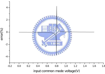
The DC response of the differential-input OTA is shown in Figure 2.14 and 2.15. In Figure 2.14, the dc transfer curve of the OTA was measured at V2=0v with three corners, tt, ff and ss, and the input common mode voltage, V1, swept from -0.8v to 0.8v. Figure 2.15 shows the dc response with V1 fixed at 0v with three corners, tt,ff and ss, and the input common mode voltage, V2, varied from -0.8v to 0.8v which is the same as Figure 2.14. In the corner “tt”, the Gm values are all about 37.5uA/V.
Figure 2.15 V-I curve of the differential-input OTA with V1 = 0V -0.2 0.0 0.2 0.4 0.6 0.8 1.0 1.2 1.4 1.6 1.8 -4 -2 0 2 4 e rro r( %)
input common mode voltage(V)
Figure 2.16 The linearity error of Gm value at different input common-mode voltages.
The linearity errors of the Gm value are defined as follow:
( ) (0) (0) = 100% (0) o in o in in I V I Gm V Gm V ε − − ⋅ (2.33)
Chapter III
Design of Tuning Circuit
3.1 Overview
As mentioned at Chapter I, one disadvantage of continuous-time filters is the requirement of additional tuning circuitry. This requirement is a result of large time-constant fluctuations due mainly to process variations. This section will present a brief overview of tuning.
3.1.1 Why Use Tuning Circuits
Analog filters must be designed with accurate component values. The resulting RC or Gm/C time-constant products are accurate to only around 30 percent with these process variations. Temperature variations worsen the situation except the process variations because resistance and transconductance values vary with temperature substantially. Thus, we need tuning circuitry to modify transconductance values such that the resulting overall time constants are set to known values[]. On chip automatic tuning of filters is a very challenging task. This chapter will present a technique to realize tuning circuitry for the integrated continuous-time filter which consists of several differential-input OTAs with large differential input signals and common-mode ranges.
3.1.2 General Concepts in Tuning
Although the transconductance value, Gmi, have large variations in their absolute value, relative transconductance values can also be set reasonably accurately. For example, if the transconductors are realized as bipolar differential pairs with an emitter degeneration resistor, then the relative transconductance values of two transconductors is set by the ratio of their respective emitter degeneration resistor.
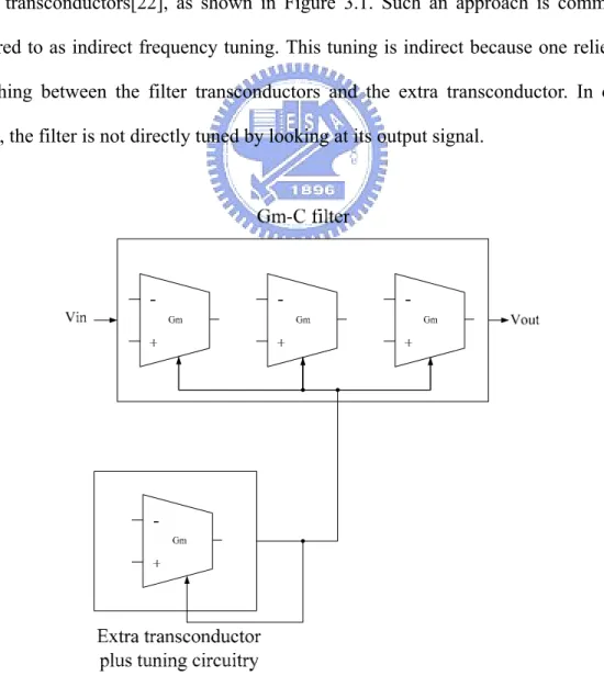
The most common way to tune a continuous-time integrated filter is to build an extra transconductor that is tuned and to use the resulting tuning signal to control the filter transconductors[22], as shown in Figure 3.1. Such an approach is commonly referred to as indirect frequency tuning. This tuning is indirect because one relies on matching between the filter transconductors and the extra transconductor. In other word, the filter is not directly tuned by looking at its output signal.
3.2 Introduction of Practicable Tuning Circuits
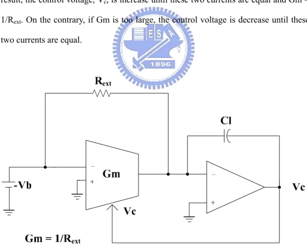
In this thesis, we use a feedback circuit to set a transconductance value equal to the inverse of an external resistance. There are several feedback circuits which can be used. Figure 3.2 and 3.3 shows two examples of constant transconductance tuning circuitry—one is voltage controlled and the other is current controlled which are assumed that the transconductor’s transconductance increases as the level of the control signal is increased. In Figure 3.2, if Gm is too small, the current through the resistor Rext is larger than the current supplied by the transconductor, and the
difference between these two currents is integrated with the opamp and capacitor. As a result, the control voltage, Vc, is increase until these two currents are equal and Gm =
1/Rext. On the contrary, if Gm is too large, the control voltage is decrease until these
two currents are equal.
In Figure 3.3, the circuit shows two voltage-to-current converters (one is the transconductor being tuned, and the other is a fixed voltage-to-current converter that simply needs a large transconductance and is not necessarily linear. This circuit operates as follows: If Gm is too small, then the voltage at the top of Rext will be less
than Vb and the fixed voltage-to-current converter will increase Icntl. At steady state,
the differential voltage into the fixed voltage-to-current converter will be zero, resulting in Gm = 1/Rext. In both circuits of Figure 3.2 and Figure 3.3, Vb is an
arbitrary voltage level, while C1 is an integrating capacitor used to maintain loop stability.
Figure 3.3 Constant transconductance tuning circuit with current controlled.
In Figure 3.2, we can replace the resistor Rext by a switch-capacitor resistor as
shown in Figure 3.4. If an accurate time period is available, a precise tuning of Gm/CA ratio can be achieved. Here, the operation of the tuning circuit shown in
Figure 3.4 is similar to the constant transconductance approaches of Figure 3.2. In addition to the external resistance which is replaced with a switched-capacitor resistance, both of them operate alike. The equivalent resistance of the switched-capacitor circuit is given by Req = 1/(fclkC), hence the transconductance
(fclk/C)/CA and then we can achieve the precise frequency tuning by just controlling
the clock signal. A disadvantage of this switched-capacitor tuning approach is that it needs large transconductance ratios between the filter’s transconductors and the tuning circuitry’s transconductor or the high frequency of the clock of the tuning circuitry. Ф1 Ф1 Ф2 Ф2 C Gm -Vb Vc Cl + _ _ Gm = fclk*C +
Figure 3.4 frequency tuning circuit
For example, consider the case of a 50-MHz filter, where the Gm/CA ratio should
be set to 2π·50MHz. We assume that the value of C and Cm is 1pF, and then Gm =
π·10-4V/A. Thus, we would require a impractical clock frequency of the switched-capacitor circuitry. In this example, fclk should be set to
-4 -12 10 314 10 clk m Gm f MHz C π× = = = (3.1)
According to this value of the clock frequency, we might consider reducing this clock frequency by increasing the value of the capacitor Cm , but although the clock
capacitance, Cm, is large. Another way to reduce the clock frequency is to set a
smaller transconductance value for the tuning circuit. For example, the transconductance value is assumed to be 0.1Gm. In this way, the clock frequency fclk is reduced by 10, Nevertheless, the filter’s transconductance values must be 10 times greater than the tuning circuitry’s transconductance value. Although the clock frequency is reduced, poorer matching occurs between the tuning circuitry and the filter. It would cause inaccurate frequency setting for the filter.
Another approach to lower the clock frequency of this switched-capacitor tuning circuitry is by using two scaled current sources, as shown in Figure 3.5. The switched-capacitor resistor is a negative equivalent resistor, and the value of the resistance can be expressed as
_ 1 -eq negative clk R f C = (3.2) .
The diode-connected transconductor is equivalent to a resistor of value 1/Gm. When the average current into the integrator is zero, Kirchhoff’s current law at the node 1 gives the equation
(
)
1 0 B clk B NI f C I Gm × × + = (3.3)And we obtain the transconductance value as follows:
clk
Gm
=
Nf C
(3.4)Considering the clock frequency fclk, the equation (2.34) can be rewritten
clk
Gm
f
NC
=
(3.5)Therefore, the clock frequency of this circuit is N times lower than the circuit shown in Figure 3.4.
Another approach to achieving frequency tuning is to use a phase-locked loop(PLL) as shown in Figure 3.6
The voltage-controlled oscillator(VCO) is realized by using transconductor-based integrators that are tuned to adjust the VCO’s frequency. After the circuit is powered up, the negative feedback of the PLL causes the VCO frequency and phase to lock to the external reference clock. Once the VCO output is locked to an external reference signal, the Gm/C ratio of the VCO is set to a desired value, and the control voltage, Vcntl, can be used to tune the integrated filter. It should be noted that choosing the external reference clock is a trade-off because it affects both the tuning accuracy as well as the tuning signal leak into the main filter. Specifically, for best matching between the tuning circuitry and the main filter, it is best to choose the reference frequency that is equal to the filter’s upper passband edge. However, noise gains for the main filter are typically the largest at the filter’s upper passband edge, and therefore the reference-signal leak into the main filter’s output might be too severe. As one moves away from the upper passband edge, the matching will be poorer, but an improved immunity to the reference signal results, Another problem with this approach is that, unless some kind of power-supply-insensitive voltage control is added to the VCO, any power-supply noise will inject jitter into the control signal, Vcntl.
3.3 Implementation of the Tuning Circuit
It was realized that a special tuning scheme need to be implemented because the differential-input OTA designed in Chapter 2 includes two different control voltages, Vcn and Vcp. In this research, we use a N-type frequency tuning circuit shown in Figure 3.7 to control the voltage[22], Vcntl, and a complementary P-type frequency tuning circuit shown in Figure 3.8 to control the voltage, Vcptl. The integrated
high frequency filter. Obviously the disadvantage (it needs large transconductance ratios between the filter’s transconductors and the tuning circuitry’s transconductor or the high frequency of the clock of the tuning circuitry) of this switched-capacitor tuning approach in this integrated continuous-time filter would not exist. The entire architecture of the frequency tuning circuitry is shown in Figure 3.9. The control voltages of the N-tuning and P-tuning circuits, Vcntl and Vcptl, are connected with the control voltages of the N-gm cell and P-gm cell, Vcn and Vcp, respectively.
In Figure 3.7, the bias voltage, Vb, is a negative voltage, and the output current flowing out of the transconductor increases as the control voltage increases. If Gm is too small, the current through the switch-capacitor resistor is larger than the current supplied by the transconductor, and the difference between these two currents is integrated with the N-op and capacitor. Therefore, the control voltage, Vcntl, is
increase until these two currents are equal and Gm = fclk*C. On the contrary, if Gm is
too large, the control voltage is decrease until these two currents are equal. In Figure 3.8, the bias voltage is replace with a positive voltage, and the N-op is replace with the P-op. The output current flowing into the transconductor increases as the control voltage, Vcptl, decreases. In the same way, if Gm is too small, the current through the switch-capacitor resistor is larger than the output current flowing into the transconductor, and the difference between these two current is integrated with the P-op and capacitor. As a result, the control voltage, Vcptl, is decrease until these two currents are equal. On the contrary, if Gm is too large, the control voltage is increase until these two currents are equal.
Figure 3.7 N-type frequency tuning circuit.
Ф
1Ф
1Ф
2Ф
2C
Gm
Vb
Vcptl
Cl
+ _ _Gm = fclk
+P-op
Figure 3.8 P-type frequency tuning circuit. .
Figure 3.9 The entire architecture of the frequency tuning circuitry.
3.4 Simulation Results of the Tuning Circuit
Figure 3.10 Transient response of the output control voltage, Vnctrl.
Figure 3.10 shows the transient response of the output control voltage, Vnctrl. This output control voltage which varies from 372mV to 384mV is stabilized at the voltage of 378mV when the amplitude of the input signal of the OTA is 0.7V. Figure 3.11 shows the transient response of the output control voltage, Vpctrl, and at the stable situation, the output voltage, Vpctrl, is -661mV with 10mV amplitude when the amplitude of the input signal of the OTA is 0.7V.
Chapter IV
Design of Continuous-Time Gm-C Filters
4.1 Fundamental Concepts of Analog Filters
A filter is a twoport that shapes the spectrum of the input signal in order to obtain an output signal with the desired frequency content. Thus, a filter has a passbands where the frequency components are transmitted to the output and stopbands where they are rejected. The oldest technology for realizing filters makes use of inductors and capacitors, and the resulting circuits are called passive LC filters. Today, in order to miniaturize the size of filters, inductors cannot be used because their size cannot be reduced to a level compatible with modern integrated electronics. Therefore, there has been considerable interest in finding filter realizations that do not require inductors. The inductors can be avoided if we have access to gain. Therefore, the only passive components we need are resistors and capacitors, and gain is provided by operational amplifiers or operational transconductance amplifiers (OTAs). Such filters are referred to as active filters, sometimes more specifically as analog active filters to distinguish them from digital filters. Signals in analog active filers are normally continuous functions of time, sometimes sampled, whereas in digital filters signals are digitized. In modern communication systems, both analog signals and digital signals must be processed. Often both analog and digital circuits and filters must be implemented together on the same integrated circuit chip for so-called mixed-mode signal processing.
4.2 LC Ladder Simulation by Signal-Flow Graphs
4.2.1 Introduction of LC Ladder Filters
Although the subject of this thesis is the design of active filters, we shall discuss some details concerning the design of passive LC filters. As the name implies, an LC filter is a lossless transmission network consisting of only inductors and capacitors. In normal operation, the network is embedded between a resistive source and a resistive load as shown in Figure 4.1, and Figure 4.2 shows the ladder topology. A lossless ladder is a circuit structure where all components apart from source and load resistors are lossless, that is, they are inductors and capacitors that dissipate no energy. Passive LC ladders have an inherent advantage over active filters in terms of their sensitivity to component tolerances. With the growing pressure towards microminiaturization, inductors were found to be too bulky so that designers started to replace passive RLC filters by active RC circuits where gain, obtained from operational amplifiers, together with resistors and capacitors in feedback networks, was used to achieve complex poles.
Figure 4.2 Resistively terminated ladder structure.
4.2.2 LC Ladder Simulation by Signal-Flow Graphs
Lossless filters designed for maximum power transfer have the best possible passband sensitivities, and such circuits are normally realized as LC ladders. A considerable amount of effort has been devoted in recent years to the development of active circuits which in one way or another simulate performance of passive ladders and thereby inherit their good sensitivity performance. Ladder simulations can be classified into two groups: operational simulation and element substitution. Both methods start from an existing LC prototype ladder; operational simulation endeavors to represent the internal operation of the ladder by simulating the equations describing the circuit’s performance, i.e., Kirchhoff’s voltage and current laws and the I-V relationships of the ladder arms. Fundamentally, this procedure is based on simulating the signal-flow graph (SFG) of the ladder where all voltages and all currents are considered signals which propagate through the circuit.
For our purposes, the signal-flow graph (SFG) method can be understood most easily by considering a section of a ladder as shown in Figure 4.3. The circuit is analyzed readily by writing Kirchhoff’s laws and the I-V relationships for the ladder arms as follows:
Figure 4.3 Section of a ladder network. n-2 n-3 n-1 n-1 n-2 n n n-1 n+1 n+1 n n+2 n+2 n+1 n+3 ... I = I - I V = V - V I = I - I V = V - V I = I - I ... (4.1) n-2 n-2 n-2 n-2 n-3 n-1 n-1 n-1 n-1 n-1 n-2 n n n n n n-1 n+1 n+1 n+1 n+1 n+1 n n+2 n+2 n+2 n+2 n+2 n+1 n+3 V = Z I = Z (I - I ) I = Y V = Y (V - V ) V = Z I = Z (I -I ) I = Y V = Y (V -V ) V = Z I = Z (I - I )
In the active simulation of this circuit, all currents and voltages are to be represented as voltage signals. In order to achieve this goal, we use a resistive scaling factor R as shown in one of these equations as an example,
n n-1 n+1 I R = I R - I R n n n n n-1 n+1 Z Z V = I R = (I R -I R) R R (4.2)
and introduce the notation
k k k k k k k k I R = V = Z = R Y R = i v z y (4.3)
are now dimensionless voltage transfer functions and that both ik and vk are voltages.
We have retained the symbol ik in order to remind ourselves of the origin of that signal as a current in the original ladder. With Equation (4.3), equation group (4.1) takes on the following form:
n-2 n-3 n-1 n-1 n-2 n n n-1 n+1 n+1 n n+2 n+2 n+1 n+3 ... = - = - = - = - = - ... i i i v v v i i i v v v i i i (4.4) n-2 n-2 n-2 n-2 n-3 n-1 n-1 n-1 n-1 n-1 n-2 n n n n n n-1 n+1 n+1 n+1 n+1 n+1 n n+2 n+2 n+2 n+2 n+2 n+1 n+3 = = ( - ) = = ( - ) = = ( - ) = = ( - ) = = ( - ) v z i z i i i y v y v v v z i z i i i y v y v v v z i z i i
This group of equations indicates that for a successful simulation we need to build voltage summers to implement Kirchhoff’s laws (e.g., to add the voltages in-1 and –in+1
to form the voltage in) and we need to realize the frequency-dependent multipliers or
transfer functions (also called transmittances) zk or yk (e.g., to convert the voltage in
into the signal vn). Assuming that the necessary circuits are available, the flow
diagram in Figure 4.4 with the indicated interconnections gives the realization of the ladder section in Figure 4.3. As is customary, we have drawn the “current signals” and their summing nodes in the top line and the “voltage signals” with their summing nodes in the bottom line.
The implementation is slightly inconvenient because it requires taking the difference of two signals. It is quite obvious that summing of signals is preferable. Figure 4.5 shows that only additions are required, and it guarantees also that all internal loop gains are negative. The SFG diagram of Figure 4.5 is also referred to as leapfrog (LF) topology; the reason for this name becomes apparent when the circuit is redrawn as shown in Figure 4.6. At this occasion we also wish to emphasize that the correct realization of the transfer function poles implies that all loop gains, such as
to be the input, vn+2 the output, and in+3 = 0, the function realized by the graph in
Figure 4.4 can be shown to equal
(
)
2 2 1 -1 -2 -3 3 2 4 1 2 3 1 2 1 1 = 1 1 1 1 1 1 1 1 1 1 n n n n n n n v z y z y z i D D D D D D D D D D + + + ⎛ ⎞ ⎜ ⎟ ⎛ ⎞ ⎜ ⎟ ⎜ ⎟ ⎛ ⎞⎜ ⎟⎜ ⎟ + ⎜ + ⎟ + ⎜ + ⎟ + ⎜ ⎟ ⎝ ⎠⎜ + ⎟⎜ + ⎟ + ⎝ ⎠⎜⎜ + ⎟⎟ + ⎝ ⎠ (4.5) where 1 1 2 1 3 -1 4 -2 n n n n n n n n D y z D z y D y z D z y 2 -1 + + + = = = =The expression shows quite clearly that the transfer function poles can be expected to be accurate if all loop gains are realized correctly. It will serve as a guide in our later implementation of general signal-flow graph filters.
Figure 4.4 Signal-flow graph block diagram representation of the ladder section in Figure 4.3.
Figure 4.5 Transformation resulting in only positive input summers.
Figure 4.6 The diagram of Figure 4.5 redrawn in the leapfrog (LF) configuration.
Example: Let’s illustrate this process on a simple fourth-order all-pole lowpass filter. Figure 4.7 shows an LC ladder with two series inductors and two shunt capacitors along with two terminating resistors. As discussed, let’s normalize all the elements by dividing them by a scaling resistor R and label
1 i i i i i i i i i i i C R c L l R R r R g I R i V v = = = = = = (4.6)
2 1 2 1 3 2 3 2 3 4 3 4 1 ( ) 1 ( ) 1 ( ) in i s L Kv v i sl r v i i sc i v sl v i sc g 4 v − = + − − = − − = − + − = − + (4.7)
Figure 4.7 Fourth-order lowpass ladder.
The corresponding signal-flow graph implementation is shown in Figure 4.8. We have introduced an arbitrary constant K at the input which multiplies all signals by K and permits us thereby to realize in the active circuit the prescribed transfer function with a gain K. At this point we have to investigate how to realize the conceptual diagram of Figure 4.8 as an active RC filter. It is apparent that we require summers as well as lossy and lossless inverting and noninverting integrators. Observe that the ladder simulation consists of a number of two-integrator loops, containing an inverting and a noninverting integrator each. The two integrators are shown in Figure 4.9 and they realize 1 1 2 2 3 o G V G V V sC G + = ± + (4.8)
where the minus sign is valid for the inverting lossy Miller integrator and the plus sign must be used for the phase-lead integrator.
1 1 s sl +r 2 1 sc − 3 1 sl 4 1 L sc g − +
Figure 4.8 Simulation flow diagram of the ladder of Figure 4.7
(a)
(b)
Figure 4.9 (a) Inverting lossy Miller integrator; (b) noninverting lossy phase-lead integrator.
Note from Figure 4.8 that the internal ladder arms are realized by lossless integrators (R3 = ∞) whereas the two end branches require lossy integrators (R3 is finite) in order
to account for load resistors. Thus, it remains only to interconnect the appropriate versions of Figure 4.9 in the manner prescribed in Figure 4.8 to arrive at the final circuit shown in Figure 4.10. At the internal output nodes, we have indicated the signals of Figure 4.8 which correspond to the voltages in the final realization.
-+ + -+ + -+ - - +
Figure 4.10 Active realization of the LC ladder of Figure 4.7.
All capacitors were chosen equal for convenience. One method for finding the values of the resistors from the known components of the LC ladder requires comparing the equations realized by Figure 4.10 with the corresponding equations, Eq. (4.7), that describe the original ladder:
1 2 3 (- ) in i G V G v i sC G + = + 2 . c p ←⎯→ 2 1 1 -in in i 2 -s s Kv v Kv v i R L sl r s R R = = + + (4.9a) 4 1 5 3 2 (- ) -v -G i G i sC + = ←⎯→c p. 2 1 3 1 2 2 -1 -1 -v ( - )i i ( -i sc sc R = = i3) (4.9b)
6 2 7 4 3 (- ) ) -i G v G v sC + = ←⎯→c p. 3 2 4 2 3 3 1 1 -i (-v v ) (-v L sl s 4) v R = + = + (4.9c) 8 3 4 9 (- ) - G i v sC G = + ←⎯→c p. 4 3 4 4 -1 -1 (- ) (- ) L L v i R sc g sc R R = = + + i3 (4.9d)
Consider the needed equality of the time constants and from the dc gain factors of the signals Vin and (-v2) in equation (4.9a), we find respectively
1 3 1 s L R C R = (4.10) 3 1 s R R K R = R (4.11) 3 2 s R R R = R (4.12)
By substituting equations (4.10) into (4.11) and (4.12), we obtain
1 1 3 1 RS L R R KR C K = = R and 1 2 3 1 S R L R R R C R = =
Note that the value of R1 determines the realized gain K. Similarly, we find from
equations (4.9b) through (4.9d): 2 4 5 2 i.e., 4 5 C CR CR C R R R R C = = = = (4.13) 3 6 7 6 7 1 i.e., 3 L L CR CR R R R R C = = = = (4.14) 4 8 4 i.e., 8 C CR C R R R C = = (4.15) and 8 4 9 8 9 i.e., L L L R R R C R R R = R = R = C R (4.16)
The scaling resistor R and the capacitor C have arbitrary values and can be chosen to obtain convenient and practical components.
4.3 Fifth-Order Elliptic Low-Pass GM-C Filter
Figure 4.11 shows a fifth-order elliptic low-pass LC-ladder prototype filter. By using signal-flow graph methods [13, 18, 25], it can be transformed into a fifth-order elliptic low-pass gm-C filter which consists of seven identical differential-input OTAs and seven capacitors. Here we will introduce a very successful and popular way which is used to transform an LC passive filter into a active Gm-C filter. The way is based on the powerful signal-flow graph (SFG) method which, after impedance scaling, treats all voltages and currents in the passive circuit as voltage signals and realizes the effect of both inductors and capacitors via integrators. For example, the voltages V1 in Figure 4.11 is obtained by integrating the difference between I1 and I2:
1 1 1 1 ( V I sC = −I2) (4.17)
Figure 4.11 Fifth-order elliptic LC lowpass filter
range[23]. Because integrators can be realized with transconductances and grounded capacitors, it stands to reason that Gm-C design methods can be adapted to the SFG procedure. Specifically, it has been shown that ladder filters with quite arbitrary branches can be implemented as Gm-C circuits where furthermore all transconductors, with the exception of possibly one, are identical and all capacitors are grounded. Inevitably, this approach is very desirable because it results in simple processing technologies. The insistence on only grounded capacitors, however, entails a penalty: the realization requires many active devices (transconductors) because floating capacitors, such as C2 in Figure 4.11, result in equations with terms proportional to s,
(
1 3)
(
2 2 2 2 2 1 1 V V)
1 3 I sC V V sL sL sC − ⎛ ⎞ = =⎜ + ⎟ ⎝ ⎠ & − (4.18)which with integrators must be realized in the form 1/(1/s). A very efficient realization with savings of a large number of transconductors can be achieved, however, if floating capacitors are acceptable[20]. Consider the typical ladder section in Figure 4.12. The relevant equations describing this circuit can be written as
(
1 1 1 2 1 1 1 1 C L V I I I I sC sC = ⋅ = − − C2)
(4.19)C
2L
2C
1C
3V
1I
1I
L2V
3I
C2I
C1where IL2 and IC2 can be expressed as:
(
1 3)
2 2 L V V I sL − = (4.20)(
1 3)
2 2 1 C V V I sC − = (4.21)By substituting equations (4.20) and (4.21) into (4.19), we obtain
(
)
(
1 1 2 2 1 1 1 L V I I sC V V sC = ⎡⎣ − − − 3)
⎤⎦ (4.22) To convert the currents into voltages for active SFG simulation, we multiply both equations in (4.20) and (4.22) by a normalizing resistor R and a transconductance value gm to obtain the expressions(
1 3)
2 2 1 L V V gm RI sL gm R − = (4.23)(
)
(
1 1 2 2 1 1 L V gm RI RI sC Rgm V sC Rgm = ⎡⎣ − − 1−V3)
⎤⎦ (4.24)which are realized by the circuits in Figure 4.13
+ + C2Rgm C1Rgm (gm/R)L2 VI1=RI1 VI2=RIL2 V1 V3 VI2=RIL2 V1 V3 gm gm
In the Figure 4.13, we have labeled: VI1=RI1 and VI2=RIL2. Let us now set R=1/gm.
From Figure 4.13, the capacitors representing the inductors are then obtained by CL=gm2L. Combining the appropriate blocks identified in Figure 4.13 in the way
specified via Figure 4.11 gives the Gm-C simulation of the fifth-order elliptic lowpass ladder in Figure 4.14. Observe that the realization is very efficient, it uses only seven capacitors and seven OTAs for the seven reactances in the original ladder, including the source and load resistors that were simulated via R=1/gm. From filter tables[21] we will find the values of the seven capacitors.
Vin Vout + + + + + + + C2 C4 C1 C3 C5 Cl2 Cl4
Figure 4.14 Gm-C SFG simulation of the circuit in Figure 4.11.
4.4 Total Harmonic Distortion (THD)
If a sinusoidal waveform is applied to a linear time-invariant system, it is known that the output will also be a sinusoidal waveform at the same frequency, but possibly
with different magnitude and phase values. However, if the same input is applied to a nonlinear system, the output signal will have frequency at harmonics of the input waveform, including the fundamental harmonic. For example, if the input signal is a 1-MHz sinusoidal waveform, the output signal will have power at the fundamental, 1 MHz, as well as at the harmonic frequencies, 2MHz, 3MHz, and so on. The total harmonic distortion (THD) of a signal is defined to be the ratio of the total power of the second and higher harmonic components to the power of the fundamental for that signal. In units of dB, THD is found using the following relation:
2 2 2 h2 h3 h4 2 f V V V THD = 10 log V ⎛ + + + ⎞ ⎜ ⎝ ⎠ " ⎟ (4.25)
where Vf is the amplitude of the fundamental and Vhi is the amplitude of the ith harmonic component. Sometimes THD is presented as a percentage value as follow:
2 2 2 h2 h3 h4 f V V V THD = 100% V + + + × " (4.26)
It should be noted that the THD value is almost always a function of the amplitude of the input signal level, and thus the corresponding signal amplitude must also be reported. Also, for practical reasons, typically the power of only the first few (say, the first 5) harmonics are included since the distortion components usually fall off quickly for higher harmonics.
4.5 Simulation Results of the Filter
After designing the low-voltage CMOS fifth-order elliptic low-pass Gm-C filter and the frequency tuning circuit, the simulation result would be shown in this section. Figure 4.15 shows the frequency response of the gm-C filter with the common-mode voltage at 0V, -0.6V, and 0.6V. In this thesis, the filter can operate at large input signals and wide common-mode voltage ranges, and the cutoff frequencies of this filter at different input common-mode voltages are about 2MHz. By using a simple way to analyze the fifth-order elliptic LC lowpass filter, suppose R1=RS and we will
know that the magnitude are always at -6dB when we input the signal with low frequency. Figure 4.16 shows the tunable range of the cutoff frequency of the filter, and the cutoff frequency range of the filter is from 1.6MHz to 2.4 MHz.
Figure 4.15 The frequency responses of the gm-C filter with the common-mode voltage at 0V, -0.6V, and 0.6V.
Figure 4.16 Tunable range of the cutoff frequency.
The Total Harmonic Distortion (THD) of the filter is shown in Figure 4.17. The THD is less than -40dB when the input peak-to-peak voltage varies from 0V to 1.4V at 100kHz frequency.
Chapter V
Post Layout Simulation Results
5.1 Post Layout Simulation Results of the OTA
The DC response of the OTA was shown in Figure 5.1 and 5.2. Figure 5.1 shows the V-I curves of the differential-input OTA with different corner at V1=0v, and Figure 5.2 shows the V-I curves of the differential-input OTA with different corner at V2=0v. The OTA circuit can operate at the input common voltage of ±0.8v with a power supply of 1.8v depending on the 0.18um UMC technology.
(a)
(c)
Figure 5.1 Post layout: DC response of the OTA with different corner (a)tt (b)ss (c) ff at V1=0v
(a)
(c)
Figure 5.2 Post layout: DC response of the OTA with different corner (a)tt (b)ss (c) ff at V2=0v
5.2 Post Layout Simulation Results of the gm-C filter
Figure 5.3 Post layout: frequency responses of the gm-C filter with the common-mode voltage at 0V, -0.6V, and 0.6V.
Figure 5.3 shows the frequency response of the gm-C filter with the common-mode voltage at 0V, -0.6V, and 0.6V, and the -3dB frequencies are all about 2MHz. The magnitude are at -6dB when we input the signal with low frequency.
Figure 5.4 Post layout: transient response of gm-C filter with 1MHz input signal.
Figure 5.5 Post layout: transient response of gm-C filter with 2MHz input signal.
The transient response of the filter was evaluated with a 1.4V peak-to-peak and 2MHz input sinusoidal signal. Figure 5.4 shows the output signal with 1.4Vpp and 1MHz input signal. The amplitude of the output signal is about a half of the amplitude of input signal. Figure 5.5 shows the output signal with 1.4Vpp and 2MHz input signal, and the amplitude is about 200mV.
Figure 5.6 FFT analysis of the filter output.
Figure 5.6 shows the FFT analysis of the output of the filter. The input is a sine wave with 100kHz frequency and 1.4Vpp, and the total harmonic distortion is below -40dB. In addition to Figure 5.6, Figure 4.16 shows total harmonic distortion of the filter for different input voltage.
Specifications Results
Process UMC 0.18µm CMOS
Mixed-Signal
Power supply ±0.9V
Filter category fifth-order elliptic low-pass gm-C filter Cutoff frequency
range 1.6MHz-2.4MHz
Dynamic input range 1.4Vpp
Input common-mode
voltage range -0.7v~0.7v
Chip area 1.16 x 0.93mm2
Power dissipation 0.75mW
A table of post layout simulation results of the fitler has been shown in Table 5.1. The results of the simulation prove that the filter is working at a cutoff frequency of 1.6MHz-2.4MHz and its input common-mode voltage and input signal ranges are ±0.7v. Figure 5.7 shows the layout of the gm-C filter including the principal part of the filter and two frequency tuning circuits and the chip area is 1.16 x 0.93mm2.
The principal part of the gm-C filter Two frequency tuning circuits.
Chapter VI
Conclusions and future research
This thesis presents a 2MHz low-voltage CMOS fifth-order elliptic low-pass gm-C filter with large differential input swings and wide common-mode ranges. By using a technique, the dynamic input range is increased to 1.4Vpp at 1.8V power supply. The frequency tuning circuitry is used to adjust the cutoff frequency of the gm-C filter, which can be tuned from 1.6MHz to 2.4MHz by changing the clock frequency of the switched-capacitor equivalent resistor. The total harmonic distortion is less than -40dB when the input peak-to-peak voltage varies from 0V to 1.4V at 100kHz frequency, and the power consumption is 0.75mW.
With the progress of the process, the power supply voltage can be decreased, but the dynamic range of circuits will diminish. Hence many researches are mainly aimed at improving the dynamic range. Besides, in the future, we have to find the way to make the other performance better, including reducing the supply voltage and power consumption, improving the linearity of OTAs and the total harmonic distortion, and increasing the tunable bandwidth range of the filter, etc.
Bibliography
[1] J. H. Botma, R. F. Wassenaar, and R. J. Wiegerink, “Simple Rail-to-Rail Low-Voltage Constant-Transconductance CMOS Input Stage in Weak Inversion,” Electron Lett., vol. 29, pp. 1145–1146, 1993.
[2] Chung-Chih Hung, Kari Halonen, Veikko Porra, and Mohammed Ismail, “Low-Voltage CMOS GM-C Filter with Rail-to-Rail Common-Mode Voltage,” IEEE 39th Midwest symposium on Circuits and Systems, Volume 2, pp.921 – 924, Aug. 18-21, 1996.
[3] Chung-Chih Hung, K. A. I. Halonen, M. Ismail, V. Porra, and A. Hyogo, ”A Low-Voltage, Low-Power CMOS Fifth-Order Elliptic GM-C Filter for Baseband Mobile, Wireless Communication,” IEEE Transactions on Circuits and Systems for Video Technology, Vol. 7, Issue 4, Aug. 1997.
[4] M. F. Li, U. Dasgupta, X. W. Zhang, and Yong Ching Lim, ”A Low-Voltage CMOS OTA with Rail-to-Rail Differential Input Range,” IEEE Transactions on Circuits and Systems I: Fundamental Theory and Applications, Vol. 47, Issue 1, pp.1 – 8, Jan. 2000.
[5] A.R. Nabavi, M.A. Mansouri Birjandi, and M. Jalali, “Low-voltage CMOS Transconductance Cell Based on Composite Cells,” Proceedings of the 15th International Conference on Microelectronics, pp.215-218, Dec. 9-11, 2003.
[6] S.-C. Huang and M. Ismail,”Linear Tunable COMFET Transconductor,” Electronics Letters, Vol. 29, Issue 5, pp.459 – 461, March 1993.
[7] Changsik Yoo, Seung-Wook Lee, and Wonchan Kim, “A ±1.5-V, 4-MHz CMOS Continuous-Time Filter with a Single-Integrator Based Tuning,”, IEEE Journal of Solid-State Circuits, Vol. 33, Issue 1, pp.18 – 27, Jan. 1998.