Effect of gate metal on polymer transistor with glass substrate
Hsin-Fei Meng, Chien-Cheng Liu, Chin-Jung Jiang, Yu-Lin Yeh, Sheng-Fu Horng, and Chain-Shu Hsu
Citation: Applied Physics Letters 89, 243503 (2006); doi: 10.1063/1.2403921
View online: http://dx.doi.org/10.1063/1.2403921
View Table of Contents: http://scitation.aip.org/content/aip/journal/apl/89/24?ver=pdfcov Published by the AIP Publishing
Articles you may be interested in
Low-voltage pentacene field-effect transistors with ultrathin polymer gate dielectrics Appl. Phys. Lett. 88, 173507 (2006); 10.1063/1.2199592
Dual input AND gate fabricated from a single channel poly(3-hexylthiophene) thin film field effect transistor J. Appl. Phys. 99, 084504 (2006); 10.1063/1.2188131
Polymer thin-film transistors fabricated by dry transfer of polymer semiconductor Appl. Phys. Lett. 86, 073505 (2005); 10.1063/1.1865347
Pentacene organic field-effect transistor on metal substrate with spin-coated smoothing layer Appl. Phys. Lett. 85, 4406 (2004); 10.1063/1.1814802
Field-effect transistors on rubrene single crystals with parylene gate insulator Appl. Phys. Lett. 82, 1739 (2003); 10.1063/1.1560869
This article is copyrighted as indicated in the article. Reuse of AIP content is subject to the terms at: http://scitation.aip.org/termsconditions. Downloaded to IP: 140.113.38.11 On: Thu, 01 May 2014 01:41:24
Effect of gate metal on polymer transistor with glass substrate
Hsin-Fei Menga兲
Institute of Physics, National Chiao Tung University, Hsinchu 300, Taiwan, Republic of China
Chien-Cheng Liu, Chin-Jung Jiang, Yu-Lin Yeh, and Sheng-Fu Horng
Department of Electric Engineering, National Tsing Hua University, Hsinchu 300, Taiwan, Republic of China
Chain-Shu Hsu
Department of Applied Chemistry, National Chiao Tung University, Hsinchu 300, Taiwan, Republic of China
共Received 11 July 2006; accepted 6 November 2006; published online 11 December 2006兲 Poly共3-hexylthiophene兲 共P3HT兲 field-effect transistors 共FETs兲 are fabricated on glass substrates with SiO2 as a gate dielectric over the gate. Indium tin oxide共ITO兲, Al, and Cr are employed as gate metals. For spin-coated FET, the mobility increases from 10−4– 10−5 cm2/ V s for ITO and Al gates to 10−2 cm2/ V s for Cr gate. After O2plasma treatment, the SiO2roughness can be made as low as 0.7 nm. The mobility is further improved up to 0.3 cm2/ V s by dip-coating P3HT.⬙Crossed rods⬙ such as morphology can be observed in dip-coated FET with high mobility, indicating high degree of self-assembly facilitated by the flat SiO2 surface over Cr gate. © 2006 American Institute of
Physics. 关DOI:10.1063/1.2403921兴
Over the recent years, organic/polymeric semiconductors have received considerable attention as the active channel materials for thin film field-effect transistors共FETs兲. In par-ticular, soluble polymer semiconductors have attracted tre-mendous interests owing to the fact that these materials can be easily spin coated to form electronics on glass or plastic substrates, with the advantages of a large-area coverage, structural flexibility, room-temperature processing, and low cost. Among the various polymers studied poly 共3-hexylthiophene兲 共P3HT兲 has become one of the most prom-ising candidates for organic field-effect transistors due to its self-assembling properties to reach relatively high mobility.1 The microstructure in P3HT is shown to be affected by re-gioregularity共RR兲,2molecular weight共MW兲,3solvent,4 film-formation method,5 and blends with small molecules6 or polymers.7,8High field-effect mobility of 0.5 cm2V s共Ref.6兲 has been demonstrated on Si substrates with high-quality thermal oxide as the gate dielectric.
It is well known that the morphology of the gate dielec-tric is a crucial factor to determine the carrier mobility in a polymer FET. Good self-assembly of P3HT occurs only on atomically smooth substrate. Thermally grown SiO2films on Si substrates have such a smooth surface and excellent insu-lating characteristics to achieve better performance than other gate dielectrics. However, from the perspective of ap-plication it is highly desirable to fabricate polymer FET over glass or plastic substrates instead of silicon due to the re-quirements of flexibility, light transparency, and low cost. Employing bottom-contact FET using glass substrate, a mo-bility of 0.06 cm2/ V s was achieved.9However, the leakage current through the gate dielectric significantly reduces the on/off ratio. Dielectric films deposited on a glass substrate by the commonly used chemical vapor deposition 共CVD兲 or sputtering methods suffer from porosity and polar groups such as Si–H, O–H, and Si–OH.10 In fact, the low thermal tolerance and uneven surface morphology of the glass
sub-strate itself partially account for the poor SiO2 quality and device performance. Our aim in this work is to demonstrate that high FET mobility and reproducibility can nevertheless be achieved on glass substrates. Even though the gate metal has no direct contact with the active polymer, it turns out that the surface of atmospheric pressure CVD 共APCVD兲 SiO2 depends sensitively on the gate metal underneath. With proper choice of gate metal the performance of polymer tran-sistor can match the best on Si substrate. Such high-performance polymer FET can be combined with polymer light-emitting diode to realize all-polymer active matrix dis-play on glass substrate.11
The P3HT batches with head-to-tail fraction greater than 98.5% and high molecular weight Mwof 84 000 are used as
received from Aldrich. 0.2m filtered solutions of P3HT in high-purity chloroform from Merck were made with concen-trations of 0.5, 0.13, 0.08, and 0.06 mg/ ml for dip coating and with a concentration of 5 mg/ ml for spin coating. Prior to filtration the solutions were always annealed to 50 ° C for at least 10 min in order to increase their solubility and attain the homogeneity of the films.
Three types of gate electrodes are studied in our cases: Indium tin oxide共ITO兲, Al, and Cr. All the three cases start from an ITO-coated glass from commercial source. For ITO gate transistors the gate electrode is defined by etching pro-cess using aqua regia共mixture of hydrochloric acid and nitric acid, HNO3: HCL : H2O = 1 : 12: 12兲. Substrates were prelimi-narily cleaned by standard wet process with acetone, isopro-panol, and de-ionized water. For the other two gate metals Al and Cr films are evaporated on top of the glass substrates as the gate electrodes. SiO2 film with 300 nm thickness is de-posited over the three kinds of gates by APCVD as the gate dielectric layer. Au source-drain contacts were thermally evaporated on top of the APCVD SiO2surface and the drain/ source electrodes of 5m channel length and 200m width were achieved using the standard photolithographic lift-off process. All the samples are treated by UV ozone to obtain hydrophilic surface. O2plasma treatment is employed to re-duce the SiO2 surface roughness. Prior to deposition of the
a兲Author to whom correspondence should be addressed; electronic mail:
meng@mail.nctu.edu.tw
APPLIED PHYSICS LETTERS 89, 243503共2006兲
0003-6951/2006/89共24兲/243503/3/$23.00 89, 243503-1 © 2006 American Institute of Physics This article is copyrighted as indicated in the article. Reuse of AIP content is subject to the terms at: http://scitation.aip.org/termsconditions. Downloaded to IP:
P3HT, the hexamethyldisilazane共HMDS兲 layer is spun on to convert the hydrophilic surface to hydrophobic surface, upon which P3HT is ready to self-assemble into microcrystalline structures.1 HMDS is then baked at a range from 30 to 110 ° C to get better adhesion and lower surface rough-ness. From the atomic force microscope共AFM兲 topographic images, there is an optimal baking temperature around 50– 70 ° C, with less clusters and better surface morphology. P3HT films are deposited on HMDS by either spin-coating or dip-spin-coating methods. In the case of dip-coated P3HT transistors, the samples are dipped vertically into the P3HT chloroform solution and extracted at a linear rate of 32m / s using a controlled stepping motor. During dip coat-ing all the samples are kept in inert atmospheres with O2/ H2O levels below 0.1 ppm. After coating, the films were dried in vacuum 共10−3torr兲 for more than 24 h to remove any residuals of solvent being used. Finally, the FET is pack-aged in N2 ambient and the FET characteristics of all samples were measured by a high impedance HP 4157 pa-rameter analyzer under ambient.
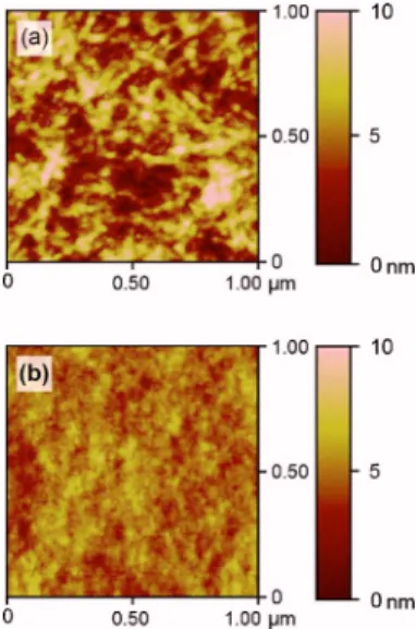
Figure 1 shows the images of SiO2 layer over various gate electrodes including共a兲 ITO, 共b兲 Al, and 共c兲 and 共d兲 Cr. Optical microscope is used for 共a兲 whereas AFM 共Digital Instruments Dimension 3100兲 is used for 共b兲, 共c兲, and 共d兲. Speckles of 100m scale can be seen in Fig.1共a兲for SiO2 over ITO. The heights of regions with different colors differ by as much as 30 nm. Such speckles show up for ITO glasses from different commercial sources with varied pat-terns. We therefore attribute this to the intrinsic chemical stability of ITO in the high-temperature reaction chamber for SiO2APCVD growth. No such large-scale speckles are ob-served for SiO2 over Al and Cr gates. However, the topo-graphic AFM image of SiO2on Al in Fig.1共b兲shows forma-tion of hillocks. The main cause of the hillocks is the large stress mismatch between Al and the glass substrate origi-nated from the difference in thermal expansion coefficients.12 Indeed, the APCVD oxide growth temperature is as high as 400 ° C. The root-mean-square roughness of SiO2 is up to 9.1 nm due to the hillocks. It turns out that the problems of ITO and Al gates can be solved by using Cr, which is chemi-cally stable during the APCVD reaction and does not exhibit hillocks on glass due to good adhesion. The AFM image of the as-grown SiO2/ Cr surface is shown in Fig. 1共c兲. The roughness becomes 2.5 nm and no hillocks are seen. Using
O2 plasma treatment, the roughness of SiO2/ Cr surface can be further reduced to as low as 0.75 nm, as shown in Fig. 1共d兲. Note that the hillocks in SiO2/ Al surface are too robust to be eliminated by O2plasma.
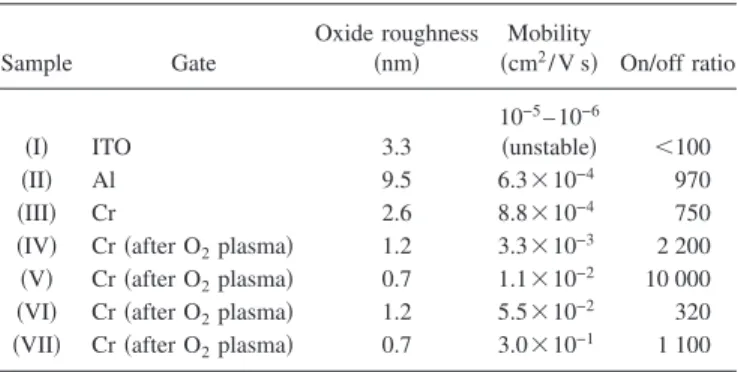
It is well known that the mobility of polymer FET is very sensitive to the interface roughness. A smooth gate di-electric promotes structure ordering in the polymer active layer, which improves the carrier mobility.13Comparison for P3HT transistor characteristics with SiO2 gate dielectric on various gate metals is shown in TableI. The field-effect mo-bility can be obtained from the saturation current Ids =共WCox/ 2L兲共Vg− V0兲2 at saturation voltage V = −40 V.
Cox= 11.13 nF / cm2is the SiO2capacitance per unit area. We first compare results for spin-coated P3HT films listed in items 共I兲-共V兲. For ITO gate the mobility is not stable and varies widely from sample to sample, presumably resulting from the speckles shown in Fig.1共a兲. The mobility is gener-ally between 10−6 and 10−5cm2/ V s, with some rare occa-sion to reach 10−3cm2/ V s. This is four orders of magnitude lower than the P3HT mobility on Si substrate. For Al gate the 9.5 nm roughness is, in fact, larger than the roughness of 3.3 nm for ITO gate but there is now no speckle. The mobil-ity is enhanced to 6.3⫻10−4cm2/ V s and is more stable. Apparently the hillocks of SiO2 over Al hinder the self-assembly of P3HT and prevent the mobility to reach higher level. For Cr gate without O2plasma treatment the roughness is 2.6 nm and the mobility is slightly above the Al gate value. The reproducibility is further improved. What is spe-cial about the SiO2on Cr is that its roughness can be signifi-cantly reduced by the O2 plasma. As the roughness is re-duced to 0.7 nm, the mobility reaches 1.1⫻10−2 cm2/ V s, only one order of magnitude lower than the Si substrate value.
The very flat SiO2surface on Cr after plasma treatment opens the possibility to an even better self-assembly of P3HT. It was shown that dip-coating process allows the poly-mer chain more time to assemble than spin-coating process because the solvent dries out rapidly in the latter. Figure2 shows carrier mobilities of P3HT transistors dip coated with various concentrations of chloroform solution. For a constant extraction speed at 32m / s, there is an optimum concentra-tion of P3HT soluconcentra-tions at 0.08 mg/ ml. This is attributed to the increased solubility at low concentration. On the other hand, when the concentration is even lower, P3HT coverage of the channel may become incomplete and the mobility drops rapidly. The transistor characteristics under optimal dip-coating extraction speed of 32m / s with 0.08 mg/ ml FIG. 1.共Color online兲 共a兲 Optical image of SiO2gate insulator surface on
ITO gate electrode.关共b兲–共d兲兴 AFM topographic images of SiO2gate
insula-tor surface based on different gate metallic electrodes.共b兲 is for Al 共rough-ness 9.5 nm兲. 共c兲 is for Cr before O2plasma treatment共roughness 2.6 nm兲.
共d兲 is for Cr after O2plasma treatment共roughness 0.75 nm兲.
TABLE I. Comparison of surface roughness of oxide, mobility, and on/off ratio with different substrate conditions and deposition methods.共I兲, 共II兲, 共III兲, 共IV兲, and 共V兲 spin-coated P3HT films; 共VI兲 and 共VII兲 dip-coated P3HT films. Sample Gate Oxide roughness 共nm兲 Mobility 共cm2/ V s兲 On/off ratio 共I兲 ITO 3.3 10−5– 10−6 共unstable兲 ⬍100 共II兲 Al 9.5 6.3⫻10−4 970 共III兲 Cr 2.6 8.8⫻10−4 750
共IV兲 Cr共after O2plasma兲 1.2 3.3⫻10−3 2 200
共V兲 Cr共after O2plasma兲 0.7 1.1⫻10−2 10 000
共VI兲 Cr共after O2plasma兲 1.2 5.5⫻10−2 320
共VII兲 Cr 共after O2plasma兲 0.7 3.0⫻10−1 1 100
243503-2 Meng et al. Appl. Phys. Lett. 89, 243503共2006兲
This article is copyrighted as indicated in the article. Reuse of AIP content is subject to the terms at: http://scitation.aip.org/termsconditions. Downloaded to IP: 140.113.38.11 On: Thu, 01 May 2014 01:41:24
chloroform solution are shown in Fig.3, with a mobility as high as 0.3 cm2/ V s. This value is about the same as the highest value reported for polymer transistor on Si substrate so far. AFM images of the surfaces of dip-coated P3HT films with O2 plasma treated oxide are shown in Fig. 4共a兲, and spin-coated P3HT films without O2plasma treated oxide are shown in Fig.4共b兲. For dip-coated P3HT surface, “rodlike” morphology can be observed 关see Fig. 4共a兲兴. The rodlike structure has been analyzed by x-ray diffraction as well as UV absorption, and is shown to possess a high degree of crystallinity formed by self-assembly of P3HT.5,14,15 Since self-assembly is very surface sensitive so far it is achieved only for silicon substrate. Our AFM images demonstrate such that polycrystalline structure is possible even for tran-sistor on rough glass substrate once the gate metal is prop-erly selected. Films with large crystalline grains in general yield higher a field-effect mobility. In contrast, no rodlike structure is observed for spin-coated film with lower mobil-ity. The transistor performances of dip-coated P3HT with two different SiO2 roughness are listed in共VI兲 and 共VII兲 of TableI.
Despite the high mobility in dip-coated devices, their on/off ratio is inferior to the spin-coated devices, as shown in TableI. As a positive Vgis applied the off-current approaches
the gate leakage current Ig, indicating that the reduced on/off
ratio is caused by the increased APCVD SiO2 conductivity after dip coating. This seems to be caused by the permeation of P3HT from the chloroform solutions to the pores of SiO2 when the sample is immersed in the solutions for a long period during dip coating. Further surface treatment for the APCVD oxide by, for example, organic monolayer is needed to reduce the permeability and maintain insulation even after dip coating.
In summary, using Cr instead of ITO or Al as the gate metal on glass substrate, we obtain very flat SiO2 gate di-electric surface free from chemical instability and hillocks. The polymer transistor mobility reaches as high as 0.3 cm2/ V s. This implies that high-performance polymer electronics can be fabricated on low-cost transparent sub-strates such as glass and plastics.
This work is supported by the National Science Council of the Republic of China, Industrial Technology Research Institute of ROC, and Chung-Hwa Picture Tubes, Ltd.
1H. Sirringhaus, N. Tessler, and R. H. Friend, Science 280, 1741共1998兲. 2Z. Bao, A. Bodabalapur, and A. J. Lovinger, Appl. Phys. Lett. 69, 4108
共1996兲.
3R. J. Kline, M. D. McGehee, E. N. Kadnikova, J. Liu, and J. J. M. Frechet,
Adv. Mater.共Weinheim, Ger.兲 15, 1519 共2003兲.
4J. F. Chang, B. Sun, and D. W. Breiby, Chem. Mater. 16, 4772共2004兲. 5G. Wang, T. Hirasa, and D. Moses, Synth. Met. 146, 127共2004兲. 6D. M. Russell, C. J. Newsome, and S. P. Li, Appl. Phys. Lett. 87, 222109
共2005兲.
7A. Babel and S. A. Jenekhe, J. Phys. Chem. B 107, 1749共2003兲. 8A. Babel and S. A. Jenekhe, Macromolecules 36, 7759共2003兲. 9G. M. Wang, D. Moses, A. J. Heeger, H. M. Zhang, M. Narasimhan, and
R. E. Demaray, J. Appl. Phys. 95, 316共2004兲.
10S. C. Deshmukh and E. S. Aydil, Appl. Phys. Lett. 65, 3185共1994兲. 11Z. L. Li, S. C. Yang, H. F. Meng, and Y. S. Chen, Appl. Phys. Lett. 84,
3558共2004兲.
12Y. Kuo, Thin Film Transistors 共Kluwer Academic, Dordrecht, 2004兲,
Chap. 5, p. 326.
13H. Sirringhaus, P. J. Brown, and R. H. Friend, Nature共London兲 14, 401
共1999兲.
14G. Wang, J. Swensen, D. Moses, and A. J. Heeger, J. Appl. Phys. 93, 6137
共2003兲.
15H. G. O. Sandberg, G. L. Frey, M. N. Shkunov, H. Sirringhaus, and R. H.
Friend, Langmuir 18, 10176共2002兲. FIG. 2. Mobility of dip-coated P3HT transistor vs the concentration of
P3HT in chloroform solution.
FIG. 3. 共Color online兲 Characteristics of P3HT FET deposited by dip-coating methods with 0.08 mg/ ml solution concentration, Cr gate, and APCVD oxide treated by O2 plasma for 15 min. Ig is the gate leakage
current.
FIG. 4. 共Color online兲 AFM image of a dip-coated P3HT film with high mobility共0.3 cm2/ V s兲 共a兲 and spin-coated P3HT film with low mobility
共10−4cm2/ V s兲 共b兲.
243503-3 Meng et al. Appl. Phys. Lett. 89, 243503共2006兲
This article is copyrighted as indicated in the article. Reuse of AIP content is subject to the terms at: http://scitation.aip.org/termsconditions. Downloaded to IP: 140.113.38.11 On: Thu, 01 May 2014 01:41:24