國 立 交 通 大 學
電子工程學系 電子研究所碩士班
碩 士 論 文
抑制熱載子劣化效應與閘極氧化層過壓之混合電壓
輸入輸出緩衝器設計
Design for Mixed-Voltage I/O Buffer against
Hot-Carrier Degradation and Gate-Oxide Reliability
研 究 生 : 蔡惠雯
指導教授 : 柯明道 教授
抑制熱載子劣化效應與閘極氧化層過壓之混合電壓
輸入輸出緩衝器設計
Design of Mixed-Voltage I/O Buffers with
Consideration for Hot-Carrier Degradation and
Gate-Oxide Overstress
研 究 生: 蔡惠雯
Student : Hui-Wen Tsai
指導教授: 柯明道 教授
Advisor : Prof. Ming-Dou Ker
國立交通大學
電子工程學系 電子研究所碩士班
碩士論文
A Thesis
Submitted to Department of Electronics Engineering & Institute of Electronics
College of Electrical Engineering and Computer Science
National Chiao-Tung University
in Partial Fulfillment of the Requirements
for the Degree of
Master
in
Electronics Engineering
Oct. 2008
Hsin-Chu, Taiwan, Republic of China
抑制熱載子劣化效應與閘極氧化層過壓之混合
電壓輸入輸出緩衝器設計
學生: 蔡惠雯 指導教授: 柯明道 教授
國立交通大學
電子工程學系 電子研究所碩士班
摘要
傳統輸出輸入介面電路部分金氧半電晶體容易在接收與傳送的轉態過程, 在汲極與源極端產生過大壓差,造成熱載子劣化效應,由於製程演進,電晶體通 道長度逐漸縮短,使得通道上電場強度越來越大,因此熱載子劣化對電晶體造成 的影響遞增,元件的使用年限也隨劣化的嚴重程度而縮短。此外,在汲極與閘極 以及源極與閘極間如何避免壓差過大導致閘極氧化層過壓問題也成為元件尺寸 下降後,在可靠度電路設計上所需面臨的挑戰。 因此在本篇論文中提出了一個具兩倍電壓耐受度之輸出輸入緩衝器,包含 串疊傳輸閘電路(stacked transmission gate) 與利用額外電路提供新接點以解 決傳統輸出輸入介面電路過大壓差之現象之新構想,並藉直接引用 N-well 極的 電壓當作閘極的一種控制邏輯簡化其電路設計上的複雜度且達到較好的面積效 能。新提出的緩衝器已實現於 1.2 伏 0.13 微米互補式金氧半製程,用以操作在 1.2V/2.5V 的混壓式介面下,其輸出頻率可達 133MHz。Design for Mixed-Voltage I/O Buffers against
Gate-Oxide Reliability and Hot-Carrier
Degradation
Student: Hui-Wen Tsai Advisor: Prof. Ming-Dou Ker
Department of Electronics Engineering & Institute of Electronics
National Chiao-Tung University
Abstract
Rapid development of complementary metal oxide semiconductor (CMOS) techniques desires the transistor dimension to scale down with lower supply voltage continually for reducing chip area, increasing operating speed, and diminishing power consumption. When thickness of gate oxide becomes much thinner and the length of MOS transistor becomes shorter corresponding to smaller device size, the decreasing maximum tolerable voltage across the transistor terminals makes the design of mixed-voltage I/O buffer facing reliability problems such as gate-oxide reliability, hot-carrier degradation, and undesired circuit leakage paths with input signal higher than the voltage level of supply voltage.
In this thesis, a new 2xVDD-tolerant I/O buffer circuit, realized with only 1xVDD devices in nanoscale CMOS technology, to prevent transistors against gate-oxide reliability and hot-carrier degradation is presented. The new proposed 2xVDD-tolerant I/O buffer has been implemented in a 130-nm CMOS process to serve a 2.5-V/1.2-V mixed-voltage interface without using the additional thick gate-oxide (2.5-V) devices. This 2xVDD-tolerant I/O buffer has been successfully confirmed by the experimental results with a signal speed of up to 133 MHz for
PCI-X application. Performances as power consumption and the robustness for hot-carrier degradation and gate-oxide overstress are also compared with a few conventional designs.
誌謝
在交通大學電子系以及研究所的這幾年,佔了目前人生將近五分之一,也是相當 重要日子,要謝謝很多很多在過程中帶給我幫助和很多很多很好的回憶的人。 首先要感謝的是我在大學專題生同時也是碩士生時的指導教授,柯明道教授,長 期以來不僅在電路研究上,科技報告撰寫上,課業上,都適時的給予我最佳的啟 發,指導和鼓勵,同時也讓我在面對問題的態度和解決事情的能力上能有更大的 進步,尤其在國外的一年更加覺得老師平日對我們學生的用心和教誨的珍貴, 能順利完成大學和碩士學業,在此要向柯教授,致上最誠摯的謝意。 另外還要感謝這兩年來學長姐們不厭其煩的教導和適時的給予我幫助。 感謝胡芳綾學姊,廖宏泰學長,在 I/O 領域等於像二個師傅一樣的傳授我好多好 多的經驗和技巧。陳世倫學長,在電路上給予我最多的啟發。陳榮昇學長,顏承 正學長,陳世宏學長,李宇軒學長,陳世範學長,在學習下線和量測晶片時,給 予我最寶貴的經驗,鼓勵和指導,蕭淵文學長,王資閔學長,在論文撰寫以及大 大小小雜事和問題處理上,一直都像大樹一樣給我寶貴的建議和幫忙。蒙國軒學 長,在課業上一直都像最好的小老師也是我要加倍努力學習的對象。還有許勝福 學長,王暢資學長,林群祐學長,賴泰翔學長,邱柏硯學長,陳志豪學長,張瑋 仁學長,曾聖峰學長,陸亭州學長,廖期聖學長,陳紹岐學長,莊介堯學長,黃 曄仁學長……等等,都給了我問題諮詢的後盾和幫忙。還有蔡佳琪同學,翁怡歆 同學,林彥良同學,溫詠儒同學,許哲綸同學,還有許筱妊同學,順維學長,晏 維學長,神童學長,萬諶學長,楊國忠學長,宗恩學長,威文學長,阿邦學長, 國維學長,小凡學長,松諭學長,巧伶學姊,國權學長,豪哥學長 以及 527, 520,307 實驗室所有所有的學長姐,同學和學弟妹們,謝謝所有的大家讓我在唸 研究所的這段時光裡,過的真的真的很快樂。 此外也要感謝大學時的同學和好朋友們一路上的打氣和鼓勵以及交通大學電子系所的老師們給予我一路上的教導和交大給予我的教育。
最後要給予最深感謝的是我的家人,謝謝他們從我出生以來的照顧和支持, 謝謝所有幫助過我陪我成長的大家,希望我能繼續加油,更認真的面對未來的一 切,在將來能有更進步的表現。
CONTENTS
ABSTRACT (CHINESE) ………..………i
ABSTRACT (ENGLISH) ………..………...ii
ACKNOWLEDGEMENT ………..iv
CONTENTS………..vi
FIGURE CAPTION………...viii
TABLE CAPTION………xi
Chapter 1 Introduction………..……….
…1
1.1
MOTIVATION
.………..1
1.2 THESIS ORGANIZATION
………..……....1
1.3 I/O BUFFER BASICS
...………..……....2
1.4 HOT-CARRER DEGRADATION CONCERN
..…………....4
1.5 GATE-OXIDE OVERSTRESS PROBLEM
………...….…..9
1.6 BRIEF INTRODUCTION OF PCI-X
………...…..9
Chapter 2 Prior I/O Circuits with 2xVDD Tolerance……...11
2.1 PRIOR DESIGN I:
A MIXED- VOLTAGE I/O BUFFER WITH TWO-STACKED NMOS, GATE-TRACKING CIRCUIT AND DYNAMIC GATE-CONTROLLED CIRCUIT……….12
2.2 PRIOR DESIGN II:
A MIX-VOLTAGE I/O BUFFER WITH TRI-STACKED TRANSISTORS TO PREVENT HOT-CARRIERDEGRADATION
……….…17
2.3 PRIOR DESIGN III:
MIX-VOLAGE I/O BUFFER WITH THIN-OXIDE AND THICK-OXIDE TRANSISTORS ……………...22
2.4 PRIOR DESIGN IV:
A MIX-VOLTAGE I/O BUFFER WITH HOT-CARRIER DEGRADATION PREVENT CIRCUIT…………...23
Chapter 3 Design of Mixed-Voltage I/O Buffer with
Consideration of Hot-Carrier and Gate-Oxide
Overstress………...30
3.1 NEW DESIGN:
A MIX-VOLTAGE I/O BUFFER WITH NEW ADDITIONAL CIRCUIT TO PREVENT HOT-CARRIER DEGRADATION AND GATE-OXIDE OVERSTRESS PROBLEMS...30
3.1.1
New Proposed Blocks………...30
3.1.2
Simulation Results………...33
3.1.3
Experimental Results………...41
Chapter 4 Conclusion and Future Work………...46
REFERENCES…………....………….………...47
FIGURE CAPTIONS
Fig. 1.1 Conventional tri-state I/O buffer used to transmit 0-to-VDD output signal or to receive 0-to-2xVDD input signal………...2 Fig. 1.2 Basic schematic for mixed-voltage I/O buffer realized with only thin-oxide
devices ……….3 Fig. 1.3 The mechanism of hot-carrier effect depicted of a typical
enhancement-mode n-channel MOS transistor………5 Fig. 1.4 Channel-hot-carrier lifetime as a function of Vds and Vgs (typical behavior for 0.25-μm CMOS process)………..…….7 Fig. 2.1 The conventional mixed-voltage I/O buffer designed with gate-tracking
circuit and dynamic n-well bias circuit to solve gate-oxide reliability
issue………12 Fig. 2.2 Drain-to-source voltage (Vds) of MN0 (and also the source-to-gate voltage
(Vsg) of transistor MP5) in Fig. 2.1 during the transition from receiving 2xVDD input signal to transmitting 0-V output signal………...15 Fig. 2.3. Drain-to-source voltage (Vds) of transistor MN3 in Fig. 2.1 (a) during the
transition from receiving 2xVDD input signal to transmitting 0-V output signal and (b) during the transition from receiving 2xVDD input signal to transmitting VDD output signal………...16 Fig. 2.4. Drain-to-source voltage (Vds) of MN2 (source-to-drain voltage (Vsd)) of
MP2 in Fig. 2.1 during the transition from receiving 2xVDD input signal to transmitting VDD output signal……….17 Fig. 2.5. Modified mixed-voltage I/O buffer designed with three-stacked transistors to prevent hot-carrier degradation………..18
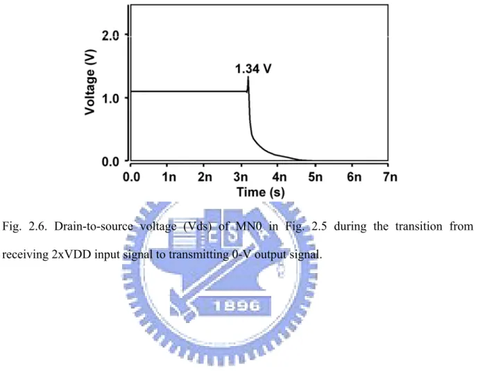
Fig. 2.6. Drain-to-source voltage (Vds) of MN0 in Fig. 2.5 during the transition from receiving 2xVDD input signal to transmitting 0-V output signal….19 Fig. 2.7. Drain-to-source voltage (Vds) of MN3 in Fig. 2.5 during the transition
from receiving 2xVDD input signal (a) to transmitting 0-V output signal and (b) to transmitting VDD output signal………20 Fig. 2.8. Source-to-gate voltage (Vsg) of MP1 in Fig. 2.5 during the transition from receiving 2xVDD input signal to transmitting 0 output signal…………..21 Fig. 2.9. Drain-to-source voltage (Vds) of MN2/MP2 in Fig. 2.5 during the
transition from receiving 2xVDD input signal to transmitting VDD output signal………..21 Fig. 2.10 Mixed-voltage I/O buffer designed with dual-oxide devices and external
n-well bias to prevent reliability issues………..23 Fig. 2.11 Design concept to overcome the hot-carrier issue in the 2xVDD-tolerant
I/O buffer with only two-stacked transistors………....24 Fig. 2.12 The implementation of the hot-carrier-prevented circuit for
2xVDD-tolerant I/O buffer with two-stacked transistors……….…25 Fig. 2.13 Hot-carrier-prevented circuits (a) for MN0, (b) for MN3, and (c) for MN2 and MP2………27 Fig. 2.14. Whole mixed-voltage I/O buffer with the hot-carrier-prevented circuits..28 Fig. 3.1 New proposed 2xVDD-tolerant I/O buffer realized with only 1xVDD
devices to prevent transistors against gate-oxide overstress and hot-carrier degradation………..30 Fig. 3.2 Simulated waveforms of the proposed mixed I/O buffer (this invention)
operating at 150 MHz when receiving 2.5-V to 0-V input signals at I/O PAD………...34
Fig. 3.3 Simulated waveforms of the proposed mixed I/O buffer (this invention) operating at 150 MHz when transmitting 1.2-V to 0-V output signals at I/O PAD………...35 Fig. 3.4 The drain-to-source voltage (Vds) of MN0 in the new proposed I/O buffer
during the transition from receiving 2xVDD input signal to transmitting 0-V output signal………...………35 Fig. 3.5 The drain-to-source voltage (Vds) of MN3 in the new proposed I/O buffer
during the transition from receiving 2xVDD input signal (a) to transmitting 0-V output signal and (b) to transmitting VDD output signal…………...…36 Fig. 3.6 The drain-to-source voltage (Vds) of transistors in the new transmitting
circuits of new proposed buffer during the transition from receiving 2xVDD input signal to transmitting VDD output signal……….37 Fig. 3.7 The gate-to-source (Vgs) voltage across transistor MP1 in the new proposed
I/O buffer during the transition from receiving 2.5-V to transmitting 0-V output signals.……….37 Fig. 3.8 (a) Layout -top- view of test chip to verify the new proposed 2xVDD-tolerant
I/O buffer in a 0.13-μm CMOS process. (b) Die photograph of the test chip for the new proposed I/O circuit fabricated with 0.13-μm 1.2-V CMOS
process………....42 Fig. 3.9 Measurement setup for the mix-voltage I/O buffer in (a) receive mode and (b)
transmit mode………...43 Fig. 3.10 Measured waveforms of the proposed 2xVDD-tolerant I/O buffer operating at VDD of 1.2 V when receiving 0-to-2.5 V input signals at I/O PAD…….44 Fig. 3.11 Measured waveforms at I/O pad of the proposed 2xVDD-tolerant I/O buffer
operating at VDD of 1.2 V when transmitting 0-to-1.2 V output signals at (a) 10 kHz and (b) 133 MHz………...45
TABLE CAPTIONS
TABLE 1.1 BASIC OPERATIONS OF 2XVDD-TOLERANT I/O BUFFER IN STEADY STATE………..……..…4
TABLE1.2 HOT CARRIER INJECTION MECHANISM AND RELATED EFFECT…………6
TABLE 2.1 OPERATIONS OF PRIOR I/O BUFFER WITH HOT-CARRIER-PREVENTED
CIRCUIT IN FIG.2.12………..………….25
TABLE3.1 COMPARISON IN AVERAGE CURRENT OF THE SUPPLY VOLTAGE AMONG
TWO PRIOR ARTS AND NEW PROPOSED I/OBUFFER IN STEADY STATE AT
85℃………38 TABLE3.2 COMPARISON IN AVERAGE CURRENT OF THE SUPPLY VOLTAGE AMONG
TWO PRIOR ARTS AND NEW PROPOSED I/O BUFFER IN CERTAIN
TRANSIENT STATE AT 85℃………39
TABLE3.3 COMPARISON IN AVERAGE CURRENT OF THE SUPPLY VOLTAGE AMONG
TWO PRIOR ARTS AND NEW PROPOSED I/OBUFFER IN STEADY STATE AT
25℃………39 TABLE3.4 COMPARISON IN AVERAGE CURRENT OF THE SUPPLY VOLTAGE AMONG
TWO PRIOR ARTS AND NEW PROPOSED I/O BUFFER IN CERTAIN
TRANSIENT STATE AT 50℃……….………39
TABLE3.5 COMPARISON ON RISE AND FALL TIME OF THE POWER SUPPLY VOLTAGE
(VDD) AMONG TWO PRIOR ARTS AND NEW PROPOSED I/O BUFFER IN
STEADY STATE AT 85℃...40
TABLE3.6COMPARISON ON PROPAGATION DELAY OF THE SUPPLY VOLTAGE AMONG
TWO PRIOR ARTS AND NEW PROPOSED I/OBUFFER IN STEADY STATE AT
Chapter 1
Introduction
1.1 M
OTIVATIONWith the rapid development of complementary metal oxide semiconductor (CMOS) technology, the transistor feature sizes have been continually scaled down to reduce chip area and increase operating speed. Besides, the normal supply voltage (VDD) to drive the chip is also reduced to save power consumption correspondingly. The gate-oxide thickness becomes much thinner in order to reduce the core power supply voltage (VDD) for resulting in lower power consumption. Meanwhile, the maximum tolerable voltages across the transistor terminals (drain, source, gate, and bulk) are correspondingly decreased to ensure lifetime. However, some earlier standardized protocols or IC chips designed and fabricated with previous CMOS processes which have higher VDD may communicate in a microelectronics system with the chips fabricated in advanced CMOS processes which has lower VDD. Therefore, the chips in advanced CMOS processes should handle the interface of input/output signals with the voltage levels higher than their normal supply voltage (VDD). Such mixed-voltage I/O interfaces must be designed to overcome several problems, such as gate-oxide reliability [1]-[2], hot-carrier degradation [3]-[5] and undesired circuit leakage paths [6].
1.2 T
HESISO
RGANIZATIONThe difficulties about hot-carrier degradation and gate-oxide overstress in prior I/O buffer design are briefed in Chapter 1 and Chapter 2. In Chapter 3, the new proposed I/O
buffer in [7] is introduced with simulation to verify the expected performance for well operating and improved robustness against hot-carrier degradation and gate-oxide overstress. Experimental results of fabricated test chip are also presented. The comparisons between several prior arts and the new proposed I/O buffer are also provided by comparing the simulated waveform and related parameters.
1.3
I/O
B
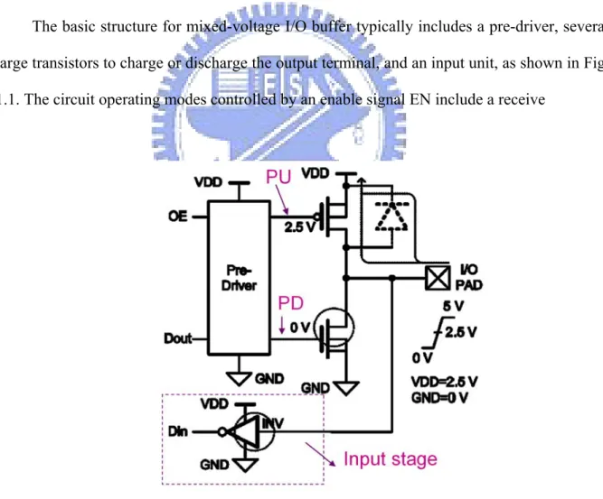
UFFERB
ASICSThe basic structure for mixed-voltage I/O buffer typically includes a pre-driver, several large transistors to charge or discharge the output terminal, and an input unit, as shown in Fig. 1.1. The circuit operating modes controlled by an enable signal EN include a receive
Fig. 1.1 Conventional tri-state I/O buffer used to transmit 0-to-VDD output signal or to receive 0-to-2xVDD input signal.
mode (for receiving an input signal) and a transmit mode (for transmitting an output signal corresponding to the data signal Dout). However, the conventional structure suffers reliability problems such as gate-oxide overstress, hot-carrier degradation, and leakage paths from I/O pad to the VDD through the drain to source and drain to bulk (parasitic pn junction) of the main driving PMOS transistor. Several designs had been proposed to solve such issues [8] to [10].
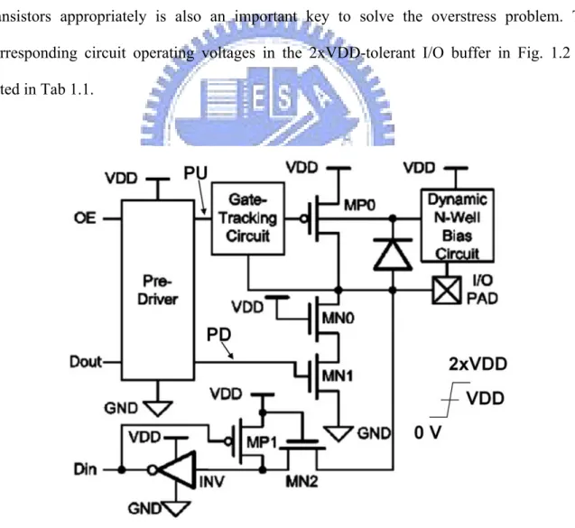
To solve the leakage problem from the I/O PAD to VDD through the parasitic pn junction in the PMOS transistor, gate-tracking and dynamic N -well bias voltage techniques had been adopted in the prior arts [8]-[10], as shown in Fig. 1.2. Placing NMOS and PMOS transistors appropriately is also an important key to solve the overstress problem. The corresponding circuit operating voltages in the 2xVDD-tolerant I/O buffer in Fig. 1.2 are listed in Tab 1.1.
TABLE 1.1
BASIC OPERATIONS OF 2XVDD-TOLERANT I/O BUFFER IN STEADY STATE
1.4
H
OT-
CARRIERD
EGRADATIONC
ONCERN1.4.1 Mechanism
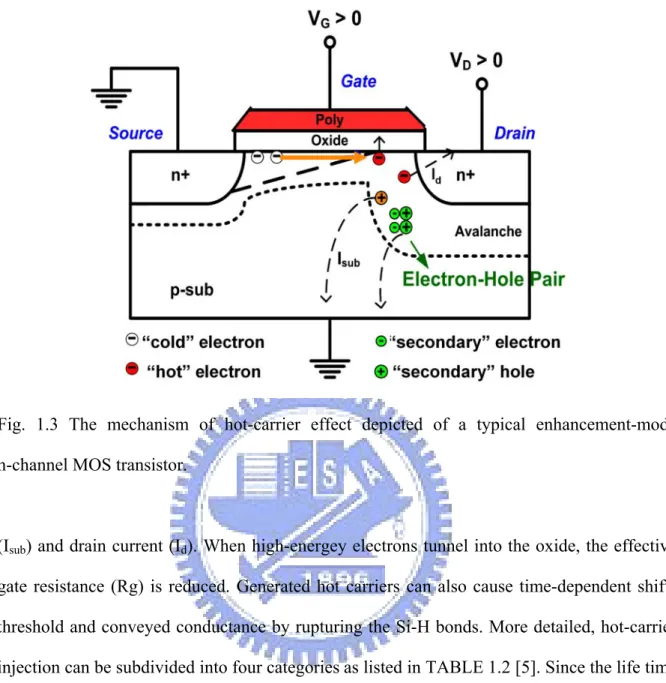
When the MOSFET devices feature extremely short channel length and high electrical field in deep-submicron technologies, hot-carrier degradation problem becomes more critical in reliability design. The mechanism of hot-carrier effect can be simply illustrated by a typical enhancement-mode n-channel MOS transistor, as shown in Fig. 1.3. With positive stress on gate and drain terminals, the electrons traveling from the source to drain gain kinetic energy while expensing electrical potential energy. When high lateral electrical field appears across drain and source terminals, electrons continually increase instant velocity and become “hot” while the average velocity saturates [11]. “Hot carriers,” including both hot electrons and hot holes but mainly hot electrons due to the larger mobility and lower interface energy barrier, can create secondary electron and hole pairs by impact ionization [12]. Collecting the secondary electrons at bulk terminal and hot electrons at drain terminals increases the value of substrate current
Operating Modes
Signals at I/O
PAD PU PD
Voltage Level of the Floating N-well
Receive Low (0 V) VDD 0 VDD
Receive High (2xVDD) VDD 0 2xVDD
Transmit Low (0 V) VDD 0 VDD
Fig. 1.3 The mechanism of hot-carrier effect depicted of a typical enhancement-mode n-channel MOS transistor.
(Isub) and drain current (Id). When high-energey electrons tunnel into the oxide, the effective gate resistance (Rg) is reduced. Generated hot carriers can also cause time-dependent shifts threshold and conveyed conductance by rupturing the Si-H bonds. More detailed, hot-carrier injection can be subdivided into four categories as listed in TABLE 1.2 [5]. Since the life time of devices, the correctness of expected operations and the performance of circuits are affected by hot carrier injection as deign parameters vary with time, it makes hot-carrier effect a non-ignorable issue, especially in design of robust mixed-voltage interface circuit in nanoscale CMOS process.
TABLE 1.2
HOT CARRIER INJECTION MECHANISM AND RELATED EFFECT
Injection Type Condition Related effect
Drain avalanche hot carrier injection (DAHC)
VD>VG (worst case at
VD=2xVG)
1. Shift of threshold voltage (Vth) 2. Shift of conductance (gm). 3. Space charge or gate current
4. Substrate’s drift current (may disturb current flow and ease latchup) Channel hot electron
injection (CHE)
VD≈VG 1. Space charge or gate current
Substrate hot electron injection (SHE)
|VB|>>0 1. Trapped charge or gate current 2. Carriers flow from substrate to oxide
Secondary generated hot electron injection (SHGE)
VD>VG |VB|>0 Impact ionization
Similar to DAHC but influenced by an extra field due to the bias voltage of substrate.
1.4.2 Lifetime Issue
Tests for the dependence of hot-carrier degradation on the device sizes had been reported in [13]. Worst stress condition of the peak substrate current (Vd=2xVg) and Vd=Vg are often seen in the tests and parameters as the degradation of the saturation drain current, ΔId/Id, Δgm/gm and ΔVth/Vth are often measured as a reference for the lifetime extrapolation in different processes.
The degradation caused by hot carriers deeply relies on the length and the biasing conditions of the device [14]. In the worse-case condition of the gate-to-source voltage (Vgs), which means the transistor is in saturation region with large drain current, the drain-to-source
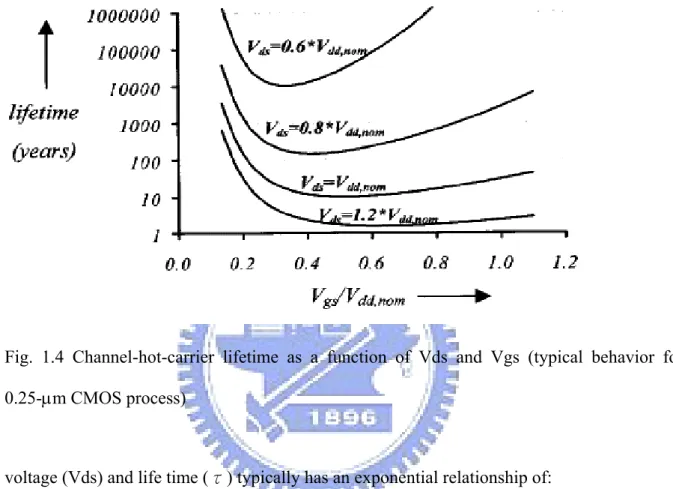
Fig. 1.4 Channel-hot-carrier lifetime as a function of Vds and Vgs (typical behavior for 0.25-μm CMOS process)
voltage (Vds) and life time (τ) typically has an exponential relationship of:
τ
life=
A
exp(
−
B V
/
ds)
(1.1),where A and B are constants, which are process-dependent.
The relationship of lifetime and the length of device are also expressed as equation 1.2: life
C
L
τ
∝
(1.2) ,where C is a constant equals 1~5.The channel length tends to have weaker effect compared with the Vds to lifetime. The relationship of lifetime and gate-to-source voltage is more complex. When the transistor is at “off” state or linear region with very high gate-to-source voltage, only little current flows in the channel and very few hot carriers are generated.
The lifetime versus drain-to source voltage (Vds) and gate-to-sourse voltage (Vgs) are depicted in Fig. 1.3 [14]. Generally, to ensure a 5~10 year life time with gate-to-source voltage (Vgs) = 0.5~1 times of power supply voltage (VDD), the drain-to-source voltage (Vds) must be kept within 1~1.1 times of power supply voltage (VDD).
1.4.3 Techniques to Increase Robustness of Circuits against Hot-carrier Degradation
Several techniques can probably be adopted in circuits to eliminate the circuit performance deterioration caused by hot-carrier effect include:
1. Methods with process modification
(1) N+ / N- double diffusion of sources and drains (2) Graded drain junctions such as LDD structure
(3)Self-aligned n- regions between the channel and the n+ junctions to create an offset gate
(4) Buried p+ channels.
2. Methods without process modifications:
(1) Different aspect ratios for the two transistors. (2) Longer channel length.
(3) Non-stationary gate voltage. (4) More stacked transistors.
In this thesis, floating n-well biasing voltage is used to provide the appropriate control voltage and reduce the number of transistors. The concept of stacked transistors technique is also adopted on transmission gate to suppress hot-carrier degradation.
1.5
G
ATE-O
XIDEO
VERSTRESSP
ROBLEMWith the advantages in speed, power and cost, thin-oxide devices are more suitable in high-speed and low-power applications. However, thin gate oxide with large gate-to-source voltage is vulnerable to gate-oxide breakdown. The breakdown can happen instantaneously or over time [15], [16]. The lifetime of gate oxide over the voltage stress can be expressed as equation 1.3 [15]. 0 0
1
*
exp(
) *
1
( )
BD efft
G X
dt
Vox t
τ
∫
−
=
(1.3),where τ0and G are two constants, Xeff is the effective thickness of the gate oxide due to the defeats, and Vox(t) is the time-dependent voltage across the gate oxide. As expressed in equation 1.3, the accumulation of the voltage stress over time determines the gate-oxide breakdown. Thus, the damage caused by transient overstress is still non-ignorable if it happens frequently and lasts for enough time.
In addition to the consideration of hot-carrier degradation, the absolute value of gate-to-source and gate-to-drain voltage should be less than the supply voltage and the drain-to-source voltage in NMOS devices and source-to-drain voltage in PMOS devices must be less than the supply voltage when devices work in “on” state.
1.5
B
RIEFI
NTRODUCTION OFPCI-X
The operating frequency used in the simulation of the new proposed I/O buffer is 133 MHz, which is the specification of PCI-X application.
PCI-X, the initial of “Peripheral Component Interconnect Extended,” is the standard for the computer bus and expansion card jointly developed by IBM, HP and Compaq [17]-[18]. With higher data width, PCI-X is an improved version of PCI for higher throughput. Such a
standard is required in some devices such as gigabit ethernet cards, fibre Channel, ultra 320 SCSI controllers, and cluster interconnects. Four frequency grades for cards or slots based on PCI-X standard are 66 MHz, 133 MHz, 266 MHz, and 533 MHz. For both PCI-X 1.0 and PCI-X 2.0, 133 MHz is included in the specifications and is most common in applications. Thus, 133 MHz is a suitable operating frequency for I/O buffer design with the expectation to be applied to the interface circuit.
Chapter 2
Prior I/O Buffers with 2xVDD Tolerance
In this chapter, three 2xVDD tolerant mixed-voltage I/O buffers ([14], [19], and [20]) and I/O buffers with dual-oxide devices are retrospected before the section of new proposed I/O buffer.
[19] was designed with eliminated reliability problems in steady state but suffers hot-carrier degradation and gate-oxide overstress problem in transient state. [14] proposed a technique which can be used to solve the hot-carrier degradation problem in stacked NMOS or PMOS transistors but it was unable to solve transient hot-carrier degradation and gate-oxide overstress happening in some transistors completely.
To realize an I/O buffer with 1.8/3.3/5-V mixed-voltage tolerance without reliability issues, 0.35-μm devices had been used in [21] and the voltage differences are kept within the supply voltage of 3.3 V. Dual-oxide (thick-oxide and thin-oxide) processes [22]-[24] had been used to prevent reliability issues in mixed-voltage in I/O buffers. Using two kinds of devices (such as 1-V and 2.5-V devices) had also been adopted in [25] to transmit 3.3-V signals without reliability issue. However, using two masks increases the cost in the fabrication.
To eliminate hot-carrier degradation and gate-oxide overstress problems in prior circuits, [20] and this work [7] are proposed. [20] will be also introduced in this chapter, and will be compared with the new proposed I/O buffer in later section.
2.1
P
RIORD
ESIGNI
A conventional mixed-voltage I/O buffer with the gate-tracking circuit and the dynamic n-well bias circuit is shown in Fig. 2.1 [19]. With the new dynamic n-well bias circuit (composed of transistor MP4 and MP6) and gate-tracking circuit (composed of transistor MN2 to MN4, transistor MP2, MP3 and MP5), this conventional I/O buffer was realized with only the thin gate-oxide devices, and it occupied smaller silicon area than the prior designs [8]-[10]. When the control signal OE is at VDD (logic “1”), the I/O buffer is operated in the transmit mode. The PD port from the pre-driver circuit is directly connected to the gate terminal of the pull-down NMOS device, MN1. The PU port of the pre-driver circuit is connected to the gate terminal of the pull-up PMOS device, MP0, through the gate-tracking circuit. According to the signal Dout controlled by the internal circuits of the IC and the turned on of transmission gate MN2
Fig. 2.1 The conventional mixed-voltage I/O buffer designed with gate-tracking circuit and dynamic n-well bias circuit to solve gate-oxide reliability issue [19].
and MP2, the PU signal and PD signal control the driving NMOS or PMOS transistors to charge I/O PAD to VDD or discharge I/O PAD to 0 V, respectively. At that time, MP4 is also
turned on to bias the floating n-well to VDD so the pn-junction diodes in transistors MP0 and MP4 are reverse biased to eliminate leakage current. When the I/O buffer is operated in the receive mode with OE signal biased at 0 V, the PU and PD ports of the pre-driver circuit are kept at VDD and 0 V, respectively. Thus, transistors MP0 and MN1 are turned off. The Din signal rises or falls according to the received signal at the I/O PAD. Transistor MP3 is used to track the signal at the I/O PAD to the gate voltage of transistor MP0 to prevent the undesired leakage current from the I/O PAD to the power supply (VDD) through the pull-up PMOS device MP0. When the voltage level at the I/O PAD exceeds VDD+|Vtp| and rise to 2xVDD, transistor MP3 is turned on to turn off transistor MP0 to prevent the leakage current through its drain to source. Transistor MP4 is also turned off while transistor MP6 is turn on to bias the floating n-well at 2xVDD to reverse bias the parasitic pn-junction diode for eradicating leakage current from the I/O PAD to VDD. Besides, MP2 is also turned off due to the turned on of transistor MP5 to eliminate the conductance and leakage current from the I/O PAD to the PU port. The input signal from the I/O PAD is transferred to the internal node Din by MN0, MP1, inverter INV1 and INV2. MN0 is used to decrease the received voltage level at the drain of MN1. Because the gate terminal of MN0 is connected to VDD, the input voltage of inverter INV is limited to VDD-Vtn when the voltage level at the I/O pad is 2xVDD. However, MP1 turns on while the input node of inverter INV1 rises over the threshold to pull down the output node of inverter INV1 to 0 V. Thus, the drain voltage of transistor MN1 is kept at VDD and the signal at the I/O pad can also be successfully received by the internal input node Din.
2.1.2 Prior Design I with Reliability Concern
Mixed-voltage I/O buffer in Fig. 2.1 can tolerate 2xVDD input signal at the I/O PAD without suffering gate-oxide reliability, hot-carrier degradation, and undesired circuit leakage
in the steady state. However, during the transition from receiving 2xVDD input signal to transmitting 0-V output signal, MN0 and MN3 suffer hot-carrier degradation problem. MP5 also suffers gate-oxide reliability problem. Moreover, MN2, MP2, and MN3 also suffer hot-carrier degradation problem during the transition from receiving 2xVDD input signal to transmitting VDD output signal.
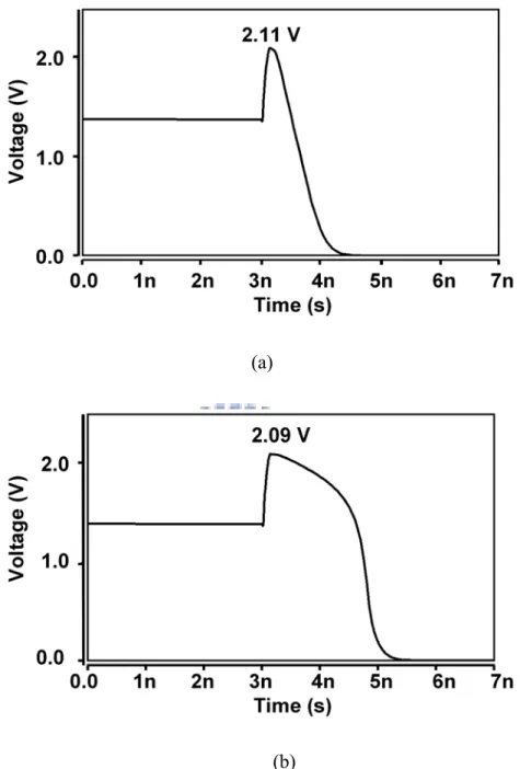
The limitations for the gate-to-source voltage and drain-to-source voltage of the transistors mentioned in the end of chapter 1 are followed in some prior arts as Fig. 2.1 in steady state. However, during the transition from receiving 2xVDD input signal to transmitting 0-V output signal, the drain-to-source voltage (Vds) of MN0 and MN3 will be much higher than VDD. The reason is that the drain-to-source voltage starts to increase from VDD since the source terminal is pulled down faster than the drain terminal at the beginning of this transition. MP5 also has larger Vgs since its source and gate are connected to the drain and source of MN0. Moreover, MN2, MP2, and MN3 also come across similar problem during the transition from receiving 2xVDD input signal to transmitting VDD output signal. While PU signal is suddenly pulled down from VDD to 0, the drain terminal of MN2 are pulled down much slower since the transistors are turned on accordingly and it also takes time for the gate terminal of MP2 to be pulled down from 2xVDD to turn on MP2. The above mentioned transient situations for MN0, MN3, MP5, MN2, and MP2 with high voltage across drain and source terminals are verified by HSPICE simulation results in a 0.13-μm CMOS technology with 1.2-V VDD and 2.5-V 2xVDD. As shown in Fig. 2.2, Fig. 2.3(a), (b), and Fig. 2.4, Vds of MN0 (also the Vsg of MP1), MN3, MN2, and MP2 are much larger than VDD during a certain time. The peak values are 1.96 V, 2.11 V, 2.09 V, and 2.07 V respectively. Thereby, it results in serious hot-carrier degradation or gate-oxide overstress in the transition from receiving 2.5-V input signal to transmitting 0-V or 1.2-V output signal.
Fig. 2.2 Drain-to-source voltage (Vds) of MN0 (and also the source-to-gate voltage (Vsg) of transistor MP5) in Fig. 2.1 during the transition from receiving 2xVDD input signal to transmitting 0-V output signal.
(a)
(b)
Fig. 2.3. Drain-to-source voltage (Vds) of transistor MN3 in Fig. 2.1 (a) during the transition from receiving 2xVDD input signal to transmitting 0-V output signal and (b) during the transition from receiving 2xVDD input signal to transmitting VDD output signal.
Fig. 2.4. Drain-to-source voltage (Vds) of MN2 (source-to-drain voltage (Vsd)) of MP2 in Fig. 2.1 during the transition from receiving 2xVDD input signal to transmitting VDD output signal.
2.2
P
RIORD
ESIGNII
2.2.1 Basic Operation
To solve the hot-carrier degradation problems happened in some prior arts as Fig. 2.1, a technique with three or more stacked NMOS transistors and related PMOS transistors as gate control circuits had been reported in [14]. A modified 2xVDD-tolerant I/O buffer with this technique to eliminate hot-carrier issue is shown in Fig. 2.5 with similar steady state operation as listed in TABLE 1.1. When the I/O buffer receives 2xVDD input signal, the gate terminal of MN5 and MN6 are biased at 2xVDD through MPT1 and MPT3, respectively. On the other hand, the gate terminal of transistor MN5 and MN6 are biased at VDD if a VDD signal is transmitted or a 0-V signal appears at the I/O PAD whether received or transmitted.
Fig. 2.5. Modified mixed-voltage I/O buffer designed with three-stacked transistors to prevent hot-carrier degradation [14].
2.2.2 Prior Design Ⅱ with Reliability Concern
During the transition from receiving 2xVDD input signal to transmitting 0-V output signal, the source terminal of MN5 and MN6 are biased at 2xVDD-ΔV initially (where ΔV is the Vds of the diode-connected transistors) because of their diode connected structure. Meanwhile, the source terminal of MN0 and MN3 are pulled down by MN1 and MN4 in a 0.13-μm technology, respectively. Comparing the MN0 and MN3 in Fig. 2.1 with the same transistors in I/O buffer in Fig. 2.5 during this transient time, the transistors in I/O buffer in Fig. 2.5 have smaller Vds since the drain voltage is initially smaller by –ΔV.
Fig. 2.6, Fig. 2.7(a), (b), Fig. 2.8 and Fig. 2.9 are the HSPICE simulation results using 0.13-μm CMOS technology when VDD is 1.2 V. With smaller maximum of Vds, the I/O buffer in Fig. 2.5 can almost eliminate most serious hot-carrier degradation happened in previous designs, as shown in Fig. 2.6, Fig. 2.7(a), and (b). However, the gate-oxide
overstress still happens in MP1 in Fig. 2.5 during the transition from receiving 2xVDD to transmitting 0 V, as shown in Fig. 2.8. Also, the transmission circuit (with MN2 and MP2 in Fig. 2.5) still suffers the hot-carrier degradation, as shown in Fig. 2.9.
Fig. 2.6. Drain-to-source voltage (Vds) of MN0 in Fig. 2.5 during the transition from receiving 2xVDD input signal to transmitting 0-V output signal.
(a)
(b)
Fig. 2.7. Drain-to-source voltage (Vds) of MN3 in Fig. 2.5 during the transition from receiving 2xVDD input signal (a) to transmitting 0-V output signal and (b) to transmitting VDD output signal.
Fig. 2.8. Source-to-gate voltage (Vsg) of MP1 in Fig. 2.5 during the transition from receiving 2xVDD input signal to transmitting 0 output signal
Fig. 2.9. Drain-to-source voltage (Vds) of MN2/MP2 in Fig. 2.5 during the transition from receiving 2xVDD input signal to transmitting VDD output signal.
2.3
P
RIORD
ESIGNIII
Using dual-oxide (thick-oxide and thin-oxide) process [22]-[24] provided by foundry is also a method to eliminate reliability issues as gate-oxide overstress and hot-carrier degradation in mixed-voltage I/O buffers. From equation 1.2 and 1.3, increasing channel length and gate-oxide thickness leads to increased tolerance of absolute drain-to-source and gate-to-source voltage are increased. With such a characteristic, thick-oxide devices with longer channel length are more robust than the thin-oxide device and can be used to sustain large drain-to-source or gate-to-source voltage. For example, [21] used 0.35-μm devices with voltage differences kept within the supply voltage of 3.3 V to realize an I/O buffer with 1.8/3.3/5-V mixed-voltage tolerance without reliability issues. Two kinds of devices (1-V and 2.5-V transistors) had been also adopted in [25] to output 3.3-V signal without aforesaid issues.
In the 2xVDD tolerant I/O buffer, Fig. 2.10 shows the mixed-voltage I/O buffer with dual-oxide (thick-oxide and thin-oxide) devices. An external n-well bias voltage is also connected to the body terminal of the pull-up PMOS device in the I/O buffer to avoid leakage current path from the I/O pad to the power supply (VDD) through the parasitic drain-to-well pn-junction diode. However, adding an external bias voltage VDDH requires an extra pad and another power supply, which results in increased silicon area and the cost of the whole system. Threshold voltage of the pull-up PMOS device is also increased due to the body effect with non-zero body-to-source voltage (VDDH-VDD). Therefore, the n-well biasing circuit can be replaced with the dynamic n-well bias circuit as shown in Fig. 2.1 for providing appropriate body bias. Besides, a gate-tracking circuit is still needed to avoid the leakage current path induced by the incorrect conduction of the pull-up PMOS transistor.
Fig. 2.10 Mixed-voltage I/O buffer designed with dual-oxide devices and external n-well bias to prevent reliability issues.
The thick-oxide device with longer channel length can sustain higher gate-to-source and drain-to-source voltage and the thin-oxide device has higher driving capacity under same device dimension. Therefore, core circuits can be designed with thin-oxide devices to decrease the chip area and power consumption but the I/O circuits can be designed with thick-oxide devices to avoid the gate-oxide reliability issue. However, using dual-oxide process requires two masks in the fabrication of the circuit and extra cost.
2.4
P
RIORD
ESIGNIV
2.4.1 Basic Operation
2xVDD-tolerant I/O buffer with two-stacked transistors is proposed in [20] and the concept is shown in Fig. 2.11. This design uses an extra tracking circuit to decide whether the I/O PAD is conducted to VDD or not. The tracking circuit with switch SW0 is used to speed up the voltage drop from 2xVDD to VDD at the I/O PAD when the I/O buffer is in transient state from receiving 2xVDD signal to transmit 0-V or VDD signal. A delay element is inserted between the PD port and the gate terminal of MN1 to let MN1 receive a delayed PD signal from the pre-driver.
During transition from receiving 2xVDD input signal to transmitting 0-V output signal, with the change of the enable signal OE from 0 V to VDD, the control signal VCTRL will turn on the switch SW0 to pull down I/O PAD to VDD. If the inserted delay is long enough, the I/O PAD is pulled down to VDD before the MN1 is turned on.
Fig. 2.11 Design concept to overcome the hot-carrier issue in the 2xVDD-tolerant I/O buffer with only two-stacked transistors [20].
The hot-carrier-prevented circuits (including the tracking circuit and switch) and delay element in this prior buffer are shown in Fig. 2.12, where other non-modified parts are
omitted. All bulks of PMOS transistors in the hot-carrier-prevented circuits are connected to the dynamic-biased n-well to avoid leakage paths. The switch SW0 is realized by the PMOS transistor MP7 with a tracking circuit controlled by the OE signal. Inverter chain and an additional capacitance are used to implement the delay element. The tracking circuit includes MP8, MP9, MN5, and a level shifter which shifts the voltage level of its input signal from 0-to-VDD swing to VDD-to-2xVDD swing. The corresponding voltages in steady states (transmit and receive modes) of the prior I/O buffer in Fig. 2.12 are listed in TABLE 2-1.
Fig. 2.12 The implementation of the hot-carrier-prevented circuit for 2xVDD-tolerant I/O buffer with two-stacked transistors.
TABLE 2.1
OPERATIONS OF PRIOR I/OBUFFER WITH HOT-CARRIER-PREVENTED CIRCUIT IN FIG.2.12
Modes OE I/O PAD VCTRL
Receive
0 V
0 V VDD
Receive 2xVDD 2xVDD
2.4.2 Prior Design IV with Reliability Concern
With drain voltage drops earlier and the source voltage drops later than the original design, the drain-to-source voltage of MN0 during such transition is within VDD. In the receive mode and transmit mode, the switch SW0 must be kept off in all states except the high-to-low transition to avoid interfering the steady state operation of the I/O buffer. Hence, this prior circuit in Fig. 2.11 does not suffer serious hot-carrier degradation.
When the I/O buffer in Fig. 2.12 is at the transition from receiving 2xVDD input signal to transmitting 0-V output signal, the gate voltage of MN1 is initially kept at 0 V while the PD signal is changing from 0 V to VDD. In the meantime, the VCTRL is set to VDD by turning on MN5 with 2xVDD gate voltage. Consequently, MP7 is turned on to discharge the initial voltage of 2xVDD at the I/O PAD until the voltage at I/O PAD is pulled down to ~VDD. The gate voltage of MN1 is also pulled up to VDD after the delay from the inverter chain and pulls down the I/O PAD voltage to 0 V. Thus, the drain-to-source voltage of MN0 can be kept less than VDD during the transient states.
(a)
(b)
(c)
Fig. 2.13 Hot-carrier-prevented circuits (a) for MN0, (b) for MN3, and (c) for MN2 and MP2.
Fig. 2.14. Whole mixed-voltage I/O buffer with the hot-carrier-prevented circuits [17].
The hot-carrier-prevented circuits are shown in Fig. 2.13.By applying the structure in Fig. 2.13 to the corresponding node in Figs. 2.12, the 2xVDD-tolerant I/O buffer without suffering serious reliability issues is shown in Fig. 2.14.
2.4.3 Discussion for Prior Design IV
Although prior design IV solves the serious hot-carrier degradation and gate-oxide overstress problems, it requires larger area to adopt the hot-carrier prevented circuits to the corresponding nodes. The VDDH voltage used in the level shifter also contributes to extra power and chip area. If the bulk voltage of each PMOS transistors in the hot-carrier prevented circuit is biased by the dynamic n-well circuit, the effective capacitance in the floating n-well point will be much larger which will increase the power consumption in the received mode since the VDD to 2xVDD swing in the n-well biasing circuit indicates that the effective large capacitor in the N-well is charged to 2xVDD or discharged to VDD by received signal continually. Tape buffers are usually inserted between the ideal pulse signal and the I/O PAD to provide a more practical input to I/O buffer. However, the HSPICE-simulated results of
power consumption for I/O buffer in the receive mode in HSPICE simulation is probably not so confident since merely inserting the tape buffer can not represent the real situation happens in I/O PAD in receive mode. This prior art is complex to realize reliability problem prevented circuit. When considering process-voltage-temperature (PVT) variation, the prior design IV may be affected more than prior art I, II and III. With the above concerns in prior design IV, a new 2xVDD tolerant mixed-voltage I/O buffer is proposed in the following chapter.
Chapter 3
Design of Mixed-Voltage I/O Buffer with Consideration of
Hot-Carrier and Gate-Oxide Overstress
3.1
N
EWD
ESIGN3.1.1 New Proposed Blocks
The new proposed 2xVDD-tolerant I/O buffer realized with only 1xVDD devices to prevent transistors against gate-oxide overstress and hot-carrier degradation is shown in Fig. 3.1, which keeps the significant design advantages of the prior arts with three additional new modifications. The design concepts of the major parts in this new proposed I/O buffer are introduced in the following.
Fig. 3.1 New proposed 2xVDD-tolerant I/O buffer realized with only 1xVDD devices to prevent transistors against gate-oxide overstress and hot-carrier degradation.
A. Circuit Operation
The basic structure for this mixed-voltage I/O buffer typically includes a pre-driver, a dynamic n-well bias circuit, two or three-stacked transistors, gate-tracking circuit, and an input stage unit, which is controlled by an enable signal OE. The circuit operating modes include a receive mode (for receiving input signal from I/O PAD) and a transmit mode (for transmitting output signal to I/O PAD). The corresponding steady-state circuit operating voltages in the proposed 2xVDD-tolerant I/O buffer circuit in Fig. 3.1 are listed in TABLE 2.1 in section 1.3.
B. Gate Control Circuit
Dynamic floating n-well technique is applied to the mixed-voltage I/O circuit to prevent the possible leakage current path in the PMOS transistors of the pull-up network. By surveying the voltage waveform of the floating n-well, the floating n-well voltage is kept at VDD on one hand in receiving 0-V input signal from I/O PAD and in transmit mode. On the other hand, it is kept at 2xVDD for receiving input signal of 2xVDD from the I/O PAD. Such a voltage level at the floating n-well presents a similar function to the gate control signal for the top transistor (MN5 and MN6) of the three-stacked NMOS structures in Fig. 2.5. Therefore, the new gate control circuit of these transistors can be directly implemented by the dynamic floating n-well self-biased circuit to save silicon area.
C. Transmitting Circuit
The new transmitting circuit applies the “stacked” concept in both PMOS and NMOS transistors appropriately to create a new “stacked transmission gate.” As shown in Fig. 3.1, the gate terminal of MN2 is connected to VDD and the gate terminal of MN7 is connected to the floating n-well terminal, so are MN5 and MN6. Aside from NMOS transistors, the gate terminals of other two PMOS transistors, MP2 and MP7, are connected together to the drain
terminal of MN6. In the transmit mode, the transistors MN7 and MP7 serve as a transmission gate (similar to MN2 and MP2). When receiving an input signal of 2xVDD at I/O pad, transistors MP2 and MP7 are turned off and the transistors MN7 and MN2 prevent high drain-to-source voltage (Vds). During the transition from receiving an input signal of 2xVDD to transmitting an output signal of VDD, the drain voltage of transistor MN2 keeps at 2xVDD -ΔV initially due to the diode-connected transistor MN7 (where ΔV is the Vds of the diode-connected transistor MN7). Then, it keeps a lower Vds across MN2 and MP2 when the source voltage of MN2 starts to be pulled down to 0 V. Due to the lower Vds of the stacked structures, the mentioned hot-carrier degradation problem in the transmission gates of Fig. 2.1 and Fig. 2.5 does not happen in this new design. Moreover, since the gate voltage of MP2 and MP7, and the drain and source terminals of MN7 are pulled down to 0 V while the gate terminal of MP0 is pulled down to 0 V, the gate-to-source voltages and the gate-to-drain voltages of MN7, MP7, MN2 and MP2 keep in a safe region (around or lower than VDD). Thus, the new transmitting circuit does not suffer hot-carrier degradation and gate-oxide overstress problems.
D. Modification to Prevent Gate-Oxide Overstress
In Fig. 2.1, the gate terminal and the source terminal of transistor MP5 are connected to the drain terminal and the source terminal of MN0, respectively. In Fig. 2.5, the gate terminal and the source terminal of the MP1 are connected to the source terminal of MN0 and the drain terminal of MN5, respectively. During the transition from receiving an input signal of 2xVDD to transmitting an output signal of 0 V, transistor MN0 in Fig. 2.1 suffers hot-carrier degradation and the voltage difference between the drain terminal of MN5 and the source terminal of MN0 in Fig. 2.5 is much larger than VDD, therefore transistor MP5 in Fig. 2.1 and transistor MP1 in Fig. 2.5 also suffer gate-oxide reliability problem.
appropriate node instead of the original one, which is the source terminal of MN0 in Fig. 2.1 and Fig. 2.5. In Fig. 3.1, the appropriate point is realized by the additional connection of a PMOS transistor and an NMOS transistor. Transistor MN8 provides similar function as transistor MN0 with smaller size, and transistor MP8 works similarly as transistor MP5. With the similar structure, the gate terminal of transistor MP1 receives similar voltage as that of transistor MP1 in previous design. In the receive mode, the gate voltage of transistor MP1 is conducted to VDD (for 2xVDD input signal from I/O PAD) or 0 V (for 0-V input signal from I/O PAD) by transistor MN8 and MP8, respectively. In the transmit mode, the gate voltage is conducted to 0 V or VDD as the drain terminal of transistor MN1 does. However, since the gate terminal of transistor MP1 does not drop to ground as immediately as the drain terminal of transistor MN1 does, large |Vgs| value does not occur in transistor MP1. The gate voltage of transistor MP1 is pulled down gradually by MN8 and the other NMOS transistors when transition from receiving 2xVDD input signal to transmitting 0-V output signal. Thus, the new proposed design does not suffer gate-oxide reliability problem in both steady state and transient state.
3.1.2 Simulation results
A. Simulated Waveform for Steady State Operation and Verification to New Modifications
The simulated results of the new proposed 2xVDD-tolerant I/O buffer to prevent hot-carrier degradation and gate-oxide reliability have been verified by the HSPICE simulation in a 0.13-μm CMOS model with VDD of 1.2 V. Fig. 3.2 and Fig. 3.3 show the simulated waveforms of the new proposed 2xVDD-tolerant I/O buffer well operating with speed of 150 MHz in the receive mode and transmit mode, respectively. As shown in Fig. 3.2, when new proposed mixed-voltage 2xVDD I/O buffer receives 0-V and 2.5-V signal from I/O PAD, it successively outputs 1.2-V and 0-V Din signal with N-well voltage biased at 1.2 V
and 2.5 V respectively. In Fig. 3.3, as Dout signal varies between 1.2 V and 0 V, new proposed I/O buffer transmits similar swing to I/O PAD accordingly and N-well voltage keeps near 1.2 V.
Fig. 3.4 shows the Vds of MN0 in the new proposed I/O buffer from receiving 2.5-V input signal to transmitting 0-V output signal. Fig. 3.5(a) and (b) shows the Vds of MN3 in the new proposed I/O buffer from receiving 2.5-V input signal to transmitting 0-V or VDD output signal, respectively. Comparing Fig. 3.4, Fig. 3.5(a) and (b) with previous figures (Fig. 2.2, Fig. 2.3(a), (b), Fig. 2.6, Fig. 2.8(a) and (b)) correspondingly, MN0 and MN3 in Fig. 2.1 suffer serious hot-carrier degradation problem due to the larger Vds. Since the drain-to-source voltage of MN0 and MN3 are nearly the same for the new buffer shown in Fig. 3.1 and the buffer shown in Fig. 2.5, the capabilities of preventing hot-carrier degradation when receiving 2.5-V input signal are almost the same between these two buffers (Fig. 2.5 and Fig. 3.1). However, the new buffer is more efficient in area saving.
Fig. 3.2 Simulated waveforms of the proposed mixed I/O buffer (this invention) operating at 150 MHz when receiving 2.5-V to 0-V input signals at I/O PAD.
Fig. 3.3 Simulated waveforms of the proposed mixed I/O buffer (this invention) operating at 150 MHz when transmitting 1.2-V to 0-V output signals at I/O PAD.
Fig. 3.4 The drain-to-source voltage (Vds) of MN0 in the new proposed I/O buffer during the transition from receiving 2xVDD input signal to transmitting 0-V output signal.
(a)
(b)
Fig. 3.5 The drain-to-source voltage (Vds) of MN3 in the new proposed I/O buffer during the transition from receiving 2xVDD input signal (a) to transmitting 0-V output signal and (b) to transmitting VDD output signal.
Fig. 3.6 shows the Vds waveforms of the transistors in the transmitting circuit of the new proposed I/O buffer from receiving 2.5-V input signal to transmitting 1.2-V output signal. As shown in Fig. 3.6, the transistors in the new proposed I/O buffer have lower drain-to-source voltage, which is more robust to prevent hot-carrier degradation.
Fig. 3.6 The drain-to-source voltage (Vds) of transistors in the new transmitting circuits of new proposed buffer during the transition from receiving 2xVDD input signal to transmitting VDD output signal.
Fig. 3.7 shows the gate-to-source voltages of transistor MP1 in the new proposed I/O buffer. The peak |Vgs| value of similar PMOS in the prior designs is larger than VDD of 1.2 V as shown in Fig. 2.2 and Fig. 2.8. However, the Vgs of MP1 in the proposed I/O buffer is close to VDD, which is confirmed more robust than the previous designs in both hot-carrier degradation and gate-oxide reliability.
Fig. 3.7 The gate-to-source (Vgs) voltage across transistor MP1 in the new proposed I/O buffer during the transition from receiving 2.5-V to transmitting 0-V output signals.
B. Power Performance of The New Proposed I/O Buffer and Prior Arts
The power consumption is compared as listed in TABLE 3.1 to TABLE 3.2 with 0.13-μm CMOS model and adopts average current of the supply voltage as reference. The temperature is set at 85℃, 25℃ and 50℃ under Typical Typical (TT) corner simulation. The output loading capacitor is 10 pF. According to the simulated results in transmit mode and in the listed two transient states, the average current of the supply voltage is near among the three buffers but the new buffer is slightly less than the other two prior arts in transmit mode. In the receive mode, the power consumption without consideration the extra received power from I/O PAD of the new buffer is larger than the two prior arts. Another comparison is done by changing the temperature to 25℃ and 50℃ in the steady state as listed in TABLE 3.3 and TABLE 3.4, respectively. Thus, the new buffer has better power performance when operating in transmit mode and more robust in the transient states.
TABLE3.1
COMPARISON IN AVERAGE CURRENT OF THE SUPPLY VOLTAGE AMONG TWO PRIOR ARTS AND
NEW PROPOSED I/OBUFFER IN STEADY STATE AT 85℃
Mixed-voltage I/O designs Receive mode Transmit mode
Prior art in Fig. 2.1 [7] 0.68uA 2.98mA
Modified I/O buffer in Fig. 2.5 13.8uA 2.94mA
TABLE3.2
COMPARISON IN AVERAGE CURRENT OF THE SUPPLY VOLTAGE AMONG TWO PRIOR ARTS AND
NEW PROPOSED I/OBUFFER IN CERTAIN TRANSIENT STATE AT 85℃
Mixed-voltage I/O designs From receive 2.5 V to transmit 0 V
From receive 2.5 V to transmit
1.2 V
Prior art in Fig. 2.1 [7] 24.4uA 0.136mA
Modified I/O buffer in Fig. 2.5 27.1uA 0.134mA
This work 26.37uA 0.135mA
TABLE3.3
COMPARISON IN AVERAGE CURRENT OF THE SUPPLY VOLTAGE AMONG TWO PRIOR ARTS AND
NEW PROPOSED I/OBUFFER IN STEADY STATE AT 25℃
Mixed-voltage I/O designs Receive mode Transmit mode
Prior art in Fig. 2.1 [7] 9.75uA 2.91mA
Modified I/O buffer in Fig. 2.5 22.55uA 2.89mA
This work 72.22uA 2.63mA
TABLE3.4
COMPARISON IN AVERAGE CURRENT OF THE SUPPLY VOLTAGE AMONG TWO PRIOR ARTS AND
NEW PROPOSED I/OBUFFER IN CERTAIN TRANSIENT STATE AT 50℃
Mixed-voltage I/O designs From receive 2.5 V to transmit 0 V
From receive 2.5 V to transmit
1.2 V
Prior art in Fig. 2.1 [7] 3.94uA 2.94mA
Modified I/O buffer in Fig. 2.5 19.85uA 2.92mA
C. Rise Time, Fall Time and Propagation Delay of The New Proposed I/O Buffer and Prior Arts
TABLE 3.5 and TABLE 3.6 show the comparison results of the rise time (tr), fall time (tf) and the propagation delay (from high to low: tphl, from low to high: tplh, and the half average of tphl and tplh: tp) of the new proposed I/O buffer and the two prior arts. The fall time and propagation delay of the modified I/O buffer in Fig. 2.5 are slightly longer than the new proposed design and the prior art in Fig. 2.1. The reason is attributed to the additional output loading due to MPT1 and MPT0 in Fig. 2.5. Since the prior art in Fig. 2.1 uses two-stacked NMOS transistors instead of tri-stacked NMOS transistors, the effected output loading of at I/O PAD is slightly smaller than the new proposed buffer and the modified I/O buffer in Fig. 2.5. However, since the capacitor at the I/O PAD in simulation for the effective output loading, 10 pf, is the dominant part, the transition performance including rise time, fall time, and propagation delay are not significant among the three circuits.
.
TABLE3.5
COMPARISON ON RISE AND FALL TIME OF THE POWER SUPPLY VOLTAGE (VDD) AMONG TWO
PRIOR ARTS AND NEW PROPOSED I/OBUFFER IN STEADY STATE AT 85℃
Mixed-voltage I/O designs
Receive mode Transmit mode
tr tf tr tf
Prior art in Fig. 2.1 [7] 0.71 ns 0.83 ns 0.4 ns 0.79 ns Modified I/O buffer in Fig. 2.5 0.71 ns 0.86 ns 0.4 ns 1.37 ns
TABLE3.6
COMPARISON ON PROPAGATION DELAY OF THE SUPPLY VOLTAGE AMONG TWO PRIOR ARTS AND NEW PROPOSED I/OBUFFER IN STEADY STATE AT 85℃
Mixed-voltage I/O designs
Receive mode Transmit mode
Tphl tplh tp tphl tplh tp
Prior art in Fig. 2.1 [7] 0.38 ns 0.45 ns 0.42 ns 0.65 ns 0.45 ns 0.55 ns Modified I/O buffer in Fig.
2.5 0.42 ns 0.47 ns 0.45 ns 1.1 ns 0.46 ns 0.78 ns This work 0.39 ns 0.51 ns 0.45 ns 0.56 ns 0.48 ns 0.52 ns
3.1.3 Experimental Results
The new proposed mixed-voltage 2xVDD-tolerant I/O buffer has been fabricated in a 0.13-μm 1.2-V CMOS process with only thin-oxide (1.2-V) devices. The layout -top- view and the die photograph of the test chip are shown in Fig. 3.8(a) and (b) with the corresponding circuit blocks, including VDD power cell, I/O circuit, Dout pad, EN pad, Din pad, and VSS power cell. Gated-ground NMOS and gate-VDD PMOS are used in the ESD protection scheme of the proposed I/O buffer.
Fig. 3.9 shows the measurement setup for the test chip with the PCB board. The rectangular pulse signal is generated by Agilent 81110A pulse generator to output 133 MHz or 1 MHz 2.5-V or 1.2-V rectangular wave. In receive mode, OE signal is connected to 0 V. Dout is floating and the I/O PAD is connected to the pulse generator. Din PAD is connected to the oscilloscope to be observed. In transmit mode, OE signal is connected to VDD. Din PAD is floating and Dout is connected to the pulse generator. The I/O PAD is connected to the oscilloscope. Besides, to compare input and output signal of the test chip, the oscilloscope is connected to the pulse generator.
the receive mode to receive the 1-MHz input signals with voltage swing of 0-to-2.5 V at I/O PAD, where the input data has been successfully transmitted to Din with a voltage swing of 0-to-1.2 V. Fig. 3.11(a) and Fig. 3.11(b) show the measured waveforms at the I/O PAD in the transmit mode to transmit the 10-kHz and 133-MHz output signals with a voltage swing of 0-to-1.2 V given at Dout, respectively. Some imperfectness of the measured waveforms can be attributed to the buffer size in the I/O cell, parasitic and loading effect of the PCB board. Cable line, inter-connections, impedance matching of the input and output of the PCB board, oscilloscope, and wave generator also cause effects such as ripples or delay at the signals.
(a)
(b)
Fig. 3.8 (a) Layout -top- view of test chip to verify the new proposed 2xVDD-tolerant I/O buffer in a 0.13-μm CMOS process. (b) Die photograph of the test chip for the new proposed I/O circuit fabricated with 0.13-μm 1.2-V CMOS process.
(a)
(b)
Fig. 3.9 Measurement setup for the mix-voltage I/O buffer in (a) receive mode and (b) transmit mode.
Fig. 3.10 Measured waveforms of the proposed 2xVDD-tolerant I/O buffer operating at VDD of 1.2 V when receiving 0-to-2.5 V input signals at I/O PAD.
(b)
Fig. 3.11 Measured waveforms at I/O pad of the proposed 2xVDD-tolerant I/O buffer operating at VDD of 1.2 V when transmitting 0-to-1.2 V output signals at (a) 10 kHz and (b) 133 MHz.
Chapter 4
Conclusion
4.1
C
ONCLUSIONA new 2xVDD-tolerant I/O buffer against gate-oxide overstress and hot-carrier degradation has been successfully verified in a 130-nm 1.2-V CMOS process with only thin-oxide devices. The gate-to-source, gate-to- drain, and drain-to-source voltages of the transistors in the new proposed 2xVDD-tolerant I/O buffer can be kept within the normal operating voltage (VDD). The new proposed 2xVDD-tolerant I/O buffer can receive 1.2-V/2.5-V input signals or transmit 1.2-V output signals up to 133 MHz, which is compatible to the I/O specifications of PCI-X in the mixed-voltage I/O interfaces.
4.2
F
UTUREW
ORKThe estimation for the power consumption in receive mode by simulation should be improved since the results observed may be different with the measured results due to the received I/O PAD signal and related parasitic effect in reality. Measurement for the performance is required to be more complete with the layout and fabrication of other prior arts.
R
EFERENCES
[1] T. Furukawa, D. Turner, S. Mittl, M. Maloney, R. Serafin, W. Clark, L. Longenbach, and J. Howard, “Accelerated gate-oxide breakdown in mixed-voltage I/O buffers,” in Proc.
IEEE Int. Reliability Physics Symp., 1997, pp. 169−173.
[2] G. P. Singh and R. B. Salem, “High-voltage-tolerant I/O buffers with low-voltage CMOS process,” IEEE J. Solid-State Circuits, vol. 34, no. 11, pp.1512-1525, Nov. 1999.
[3] I.-C. Chen, J. Y. Choi, and C. Hu, “The effect of channel hot-carrier stressing on gate-oxide integrity in MOSFETs,” IEEE Trans. Electron Devices, vol. 35, no. 12, pp. 2253−2258, Dec. 1988.
[4] M.-S. Liang, C. Chang, W. Yang, C. Hu, and R. W. Brodersen, “Hot-carriers induced degradation in thin gate oxide MOSFETs, ” in Int. Electron Devices Meeting (IEDM)
Tech. Digest, 1983, pp. 186-189.
[5] Renesas Technology, Semiconductor Device Reliability Handbook, 5th Edition, Aug. 31, 2006.
[6] S. Voldman, “ESD protection in a mixed voltage interface and multrial disconnected power grid environment in 0.5-and 0.25-μm channel length CMOS technologies,” in Proc.
EOS/ESD Symp., 1994, pp. 125−134.
[7] H.-W. Tsai and M.-D. Ker, “Design of 2xVDD-tolerant I/O buffer with considerations of gate-oxide reliability and hot-carrier degradation,” in Proc. of IEEE Int. Conf.
Electronics, Circuits and Systems, 2007, pp. 1240-1243.
[8] H.-C. Chow, “Bidirectional buffer for mixed-voltage applications,” in Proc. IEEE Int.
Symp. Circuits Syst., 1999, pp. 270–273.
[9] R. D. Adams, R. C. Flaker, K. S. Gray, and H. L. Kalter, “CMOS offchip driver circuit,” U.S. Patent 4782250, Nov. 1, 1988.
[10] M. Takahashi, T. Sakurai, K. Sawada, K. Nogami, M. Ichida, and K. Matsuda, “3.3 V–5 V compatible I/O circuit without thick gate oxide,” in Proc. IEEE Custom Integrated
Circuits Conf., 1992, pp.23. 3. 1–23. 3. 4.
[11] B. Razavi, Design of Analog CMOS Integrated Circuit, International edition, McGraw Hall, 2001.
[12] B.-G. Streetman, and S. Banerjee, Solid State Electronic Devices, 5th ed., Prentice Hall, 2000.
[13] E. Li and S. Prasad, “Channel Width Dependence of NMOSFET Hot Carrier Degradation,” IEEE Trans. on Electron Devices, vol. 50, No. 6, pp. 1545-1548, Jun. 2003. [14] A.-J. Annema, G. J. G. M. Geelen, and P. C. de Jong, “5.5-V I/O in a 2.5-V 0.25-μm CMOS Technology,” IEEE J. Solid-State Circuits, vol. 36, no.3, pp. 528-538, Mar. 2001. [15] E. R. Minami, S. B. Kuusinen, E. Rosenbaum, P. K. Ko, and C. Hu, “Circuit-level
simulation of TDDB failure in digital CMOS circuits,” IEEE Trans. Semiconduct.
Manufact., vol. 8, no. 3, pp. 370−377, Aug. 1995.
[16] A. M. Yassine, H. E. Nariman, M. McBride, M. Uzer, and K. R. Olasupo, “Time dependent breakdown of ultrathin gate oxide,” IEEE Trans. Electron Devices, vol. 47, no. 7, pp. 1416−1420, Jul. 2000.
[17] Wikipedia : http://en.wikipedia.org/wiki/PCI-X
[18] J. Brewer and J. Sekel (2004, Jun.). White paper: PCI Express Technology. Dell Inc., US.
[Online].Avaliable:http://www.dell.com/content/topics/global.aspx/vectors/en/2004_pciex press?c=us&l=en&s=corp
[19] M.-D. Ker, S.-L. Chen, and C.-S. Tsai, “Overview and design of mixed-voltage I/O buffers with low-voltage thin-oxide CMOS transistors,” IEEE Trans. on Circuits and
[20] M.-D. Ker and F.-L. Hu, “Design on mixed-voltage I/O buffers with consideration of hot-carrier reliability,” in Proc. 2007 IEEE Int. Symp. on VLSI Design, Automation and
Test, 2007, pp. 36-39.
[21] T.-J. Lee, T.-Y. Chang, and C.-C. Wang,, “Mixed-voltage-tolerant I/O buffer design,” in
Proc. Int. Symp. on Integrated Circuit, 2007, pp. 556-559.
[22] K. Bult, “Analog broadband communication circuits in pure digital deep sub-micron CMOS,” in IEEE Int. Solid-State Circuits Conf. Dig. Tech. Papers, 1999, pp. 76-77. [23] S. Poon, C. Atwell, C. Hart, D. Kolar, C. Lage, and B. Yeargain, “A versatile 0.25
micron CMOS technology,” in Int. Electron Devices Meeting (IEDM) Tech. Digest, 1998, pp. 751-754.
[24] M. Hargrove, S. Crowder, E. Nowak, R. Logan, L. K. Han, H. Ng, A. Ray, D. Sinitsky, P. Smeys, F. Guarin, J. Oberschmidt, E. Crabbé, D. Yee, and L. Su, “High-performance sub-0.08μm CMOS with dual gate oxide and 9.7 ps inverter delay,” in Int. Electron
Devices Meeting (IEDM) Tech. Digest, 1998, pp. 627-630.
[25] S.-L. Chen and M.-D. Ker, “A new output buffer for 3.3-V PCI-X application in a 0.13-μm 1/2.5-V CMOS process,” in Proc .of IEEE Asia-Pacific conf. ASIC (AP-ASIC), 2004, pp. 112-155.
Publications:
(A) International Conference paper
[1] H.-W. Tsai and M.-D. Ker, “Design of 2xVDD-tolerant I/O buffer with considerations of gate-oxide reliability and hot-carrier degradation,” in Proc. of the 14th
IEEE International
Conference on Electronics, Circuits and Systems (ICECS 2007), Marrakech, Morocco,
Dec. 11-14, 2007, pp. 1240-1243.
(B) Regular Journal Papers paper
Submitted: H.-W. Tsai and M.-D. Ker, “Design for 2xVDD-tolerant mixed-voltage I/O buffer against gate-oxide reliability and hot-carrier degradation,” IEEE Trans. Circuits
Syst. I

![Fig. 2.5. Modified mixed-voltage I/O buffer designed with three-stacked transistors to prevent hot-carrier degradation [14]](https://thumb-ap.123doks.com/thumbv2/9libinfo/8484999.184376/31.892.131.799.109.758/modified-voltage-designed-stacked-transistors-prevent-carrier-degradation.webp)