國
立
交
通
大
學
電機資訊學院 電子與光電學程
碩
士
論
文
化學機械研磨與蝕刻製程導致微影疊對誤差變異的
影響研究與改善
The Study and Improvement of
Chemical Mechanical Planarization and
Etching Process Induced Lithography
Overlay Error Variation
研 究 生:陳峰義
指導教授:羅正忠 博士
化學機械研磨與蝕刻製程導致微影疊對誤差變異的
影響研究與改善
The Study and Improvement of Chemical
Mechanical Planarization and Etching Process
Induced Lithography Overlay Error Variation
研 究 生:陳峰義 Student:Feng-Yi Chen
指導教授:羅正忠 博士 Advisor:Dr. Jen-Chung Lou
國 立 交 通 大 學
電機資訊學院 電子與光電學程
碩 士 論 文
A Thesis
Submitted to Degree Program of Electrical
Engineering Computer Science
College of Electrical Engineering and Computer
Science
National Chiao Tung University
in Partial Fulfillment of the Requirements
for the Degree of
Master of Science
in
Electronics and Electro-Optical Engineering
June 2005
Hsinchu, Taiwan, Republic of China
中華民國九十四年七月
化學機械研磨與蝕刻製程導致微影疊對誤差變異
的影響研究與改善
學生 : 陳峰義 指導教授 : 羅正忠博士 國立交通大學電機資料學院 電子與光電學程 研究所 碩士班摘要
在 IC 製造過程中, 微影是最關鍵的製程之一, 直接關係著最小特徵尺寸的極限, 微 影即是經由對準曝光而將光罩上電路圖案轉移至晶片上適當的位置, 層間的圖案疊合差 異稱為疊對誤差, 疊對誤差過大而超過設計規範將導致元件短路或斷路,並影響產品良 率, 所以疊對誤差的最小化與持續良好控制是微影最重要的課題之一. 在現今的 IC 製程中,微影製程不再是影響疊對誤差的唯一因素,其它製程,如化學機械研 磨,蝕刻,薄膜成長等製程,也會影響微影製程的對準行為與疊對誤差結果 本論文研究主題是探討化學機械研磨與蝕刻的製程條件對微影疊對誤差造成影響的可 能原因,並透過實驗驗證之,實驗結果經由固定化學機械研磨轉向與適當增加蝕刻時間,可 以得到良好的疊對誤差控制. 最後我們探討了各晶圓製程可能造成的對準圖案異常,並提出微影對準科技可能改善的 方向. IThe Study and Improvement of Chemical Mechanical Planarization
and Etching Process Induced Lithography Overlay Error Variation
Student : Feng-Yi Chen Advisor : Dr. Jen-Chung Lou
Degree Program of Electrical Engineering Computer Science National Chiao Tung University
Abstract
Lithography is the key step of IC manufacturing and directly influences the limit of critical dimension (CD).The lithography is to transfer the pattern on mask to wafer in right position, through alignment and exposure. The pattern misplacement between the layer and its previous layer is called overlay error. Once the overlay error exceeds the limit of fault
tolerance defined by design rule will make circuit either open or short, and then suffers yield lost. Therefore, to minimize the overlay error and well to control the overlay error are always an important topic of lithography.
In advanced IC fabrication, lithography is no longer the only factor resulting in the misalignment. In fact, such as chemical mechanical planarization (CMP), etch, and thin film deposition also influence the alignment and overlay significantly. In this thesis, we discuss the possible factors affecting overlay error, such as chemical mechanical planarization and
etching process. Finally, we demonstrate the solution by unifying CMP rotary direction and increasing over-etching to achieve tighter overlay control.
III
In conclusion, we discuss the wafer process that may influence alignment mark shape. Alignment improvement strategies reducing the sensitivity with wafer process is also provided.
Acknowledgement
I would like to express sincere gratitude to my advisor, Dr. Jen-Chung Lou for his instruction, encouragement, and insightful suggestion. I learned from him not only the knowledge about semiconductor manufacture but also the appropriate attitude toward researches. Without his detailed advice, this thesis could not be finished successfully.
Appreciation is extended to my colleagues Michael Chang, Kai-Ping Chan, Li-Chung Liu, Zhi Xiang Yang for their technical assistance. Furthermore, the encouragement from my friends Dr. Yao-Hsiung Kung and Ellick Hsu is highly appreciated.
V
Contents
Chinese Abstract……….I English Abstract……… II Acknowledgement………IV Contents………V Table Captions………VII Figure Captions………VIII Chapter 1 Introduction………1Chapter 2 Background Description……….3
2.1 Overlay Error and Basics………...3
2.1.1 Definition ………..…3
2 . 2 C M P B a s i c s … … . . … … … 4
2.3 Background Description….………5
2.3.1 Definition for Abbreviations………..…5
2.4 Problem Emerge……….5
Chapter 3 Experiments and Results 3.1 Introduction of Experiments Plan………8
3.2 CMP Experiments and Results……….8
3.2.1 CMP rotary direction experiments ………... 8
3.2.2 W-CMP Over Polish Experiments and Results ………...10
3.2.3 Oxide Touch-up CMP Over Polish Experiments and Results………….10
3.2.4 The Overlay Performance after Unify CMP Rotary Direction…………11
3.2.5 Discussion for Scanner Sensitivity on ET2 etcher lots………12
3.3.1 Alignment Mark Cross Section SEM Study………14
3.3.2 ET2 Etcher Over-Etching Experiments and Results………...14
3.3.3 The Overlay Performance after Implement over etching recipe on ET2 15 3.4 CMP v.s. Etching Interaction Experiments and Results……….16
3.4.1 Discussion for CMP v.s. Etching Interaction of ET2 lot………..16
3.4.2 Experiments and Results for CMP v.s. Etching Interaction of ET2 lot...17
Chapter 4 Conclusions and Discussion……….………...18
4.1 Conclusions of Experiments……….………..18
4.2 The Discussion for Alignment and Overlay Strategies………...18
VII
Table Captions
Table 2-1 Process Flow from Contact-1 to Metal-1 lithography………22
Table 3-1 W-CMP and oxide touch up CMP rotary experiments spilt table………..22
Table 3-2 W-CMP over polish experiments spilt table………..23
Table 3-3 Oxide touch-up CMP over polish experiments spilt table……….23
Tabl2 3-4 Overlay performance by vintage summary table-1.………..23
Table 3-5 C1 over etching experiments spilt table-Lot1……….………...24
Table 3-6 C1 over etching experiments spilt table-Lot2………..………..24
Table 3-7 overlay performance by vintage summary table-2 ………..……..25
Figure Captions
Figure 2-1 Schematic of overlay offset linear items………26
Figure 2-2 Schematic of a CMP system………..………27
Figure 2-3 Schematic of erosion and dishing effect after W-CMP……….27
Figure 2-4 Schematic of Nikon Scanner System ……….………..28
Figure 2-5 Schematic of FIA Alignment System………28
Figure 2-6 Metal-1 Overlay X/Y 3 Sigma and wafer rotation baseline on ET1 and ET2……29
Figure 3-1 the wafer rotation baseline result of W-CMP and touch-up CMP experiments…..30
Figure 3-2 the wafer rotation baseline result summary of W-CMP and touch-up CMP experiments……… 31
Figure 3-3 Schematic of CMP system with two polish head………31
Figure 3-4 W-CMP Over-polish experimental results……….………...…. 32
Figure 3-5 oxide touch-up CMP over polish experimental results……….………..33
Figure 3-6 overlay X/Y 3 sigma and overlay baseline wafer rotation before and after unify the CMP rotary direction……….34
Figure 3-7 Overlay X/Y 3 Sigma and Overlay baseline wafer rotation, before and after unify the CMP rotary direction, by tool and condition vintage………35
Figure 3-8 Alignment mark cross section SEM comparison on ET1 and ET2 etchers……....36
Figure 3-9 FIA alignment signal of alignment mark 1 comparison on ET1 and ET2 etchers..37
Figure 3-10FIA alignment signal of alignment mark 2 comparison on ET1 and ET2 etchers.38 Figure 3-11 the overlay baseline result of over-etching experiments 1ot 1….………... 39
Figure 3-12 The overlay baseline result of over-etching experiments 1ot 2………..40
Figure 3-13 Overlay X/Y 3 Sigma and Overlay baseline wafer rotation, unify the CMP rotary direction and before/after ET2 over etching implement, by tool and condition vintage………...41
IX
Chapter 1
Introduction
As the IC design rule scales down continuously, the overlay tolerances becomes increasingly limited. Such tight tolerances necessitate a very high performance in alignment accuracy and overlay measurement. Not only lithography step but also other area such as CMP, etching, and film deposition influence alignment accuracy and overlay performance as well [01][02][03][04][05][06][07].
Chemical mechanical planarization of Tungsten (W-CMP) has been widely used in the planarization process. Pattern deformation poses a major challenge for lithography introduced by W-CMP process. Deformation, which induces asymmetries of alignment marks, causes errors in precise alignment. Furthermore, the film deposition thickness and the etch depth all together affect the final mark shape.
In this thesis, we study the overlay error introduced by CMP and etching process condition on the Metal-1 layer of 0.11um DRAM. In order to implement second type etcher for Contact-1 etching and maintain good Metal-1 overlay control, we have studied the effect induced by CMP rotary direction, over polishing, and over etching on the overlay baseline variation. Finally, we demonstrate the solution by unifying CMP rotary direction and increasing over-etching to achieve tighter overlay control benchmark with first type etcher lots.
2
-The thesis was organized as follow:
Chapter 1: Start with a brief introduction and a background description
Chapter 2: We describe the issue induced by second type etcher in the Contact-1 etching process. In additional, the overlay error and overlay baseline variation for Metal-1 layer resulted from two kinds of etchers are demonstrated. The possible explanation is provided.
Chapter 3: Through experiments, we discussed and verified the CMP and etching process induced overlay baseline difference. In CMP experimental section, CMP rotary direction experiment and over polish experiment were proceeded to check the CMP process induced overlay baseline difference. In etching experimental section, we check the wafer alignment mark obtained from different etcher by cross section SEM analysis. From results obtained from etcher-1 and etcher-2, we modify the process condition of etcher-2 to reduce the overlay error. Finally, to unify the rotary direction of the CMP and to increase the over etching time of etcher-2 can improve the overlay performance which is as better as that of etcher-1.
Chapter 4: Finally, some conclusions were summarized and the future work was proposed in this chapter.
Chapter 2
Background Description
2.1 Overlay Error Basics:
The integrated circuits are fabricated by patterning a sequence of masking layers, and the features on successive layers bear a spatial relationship to one another. As a part of the
fabrication process, each layer must be aligned to the previous layers. The pattern
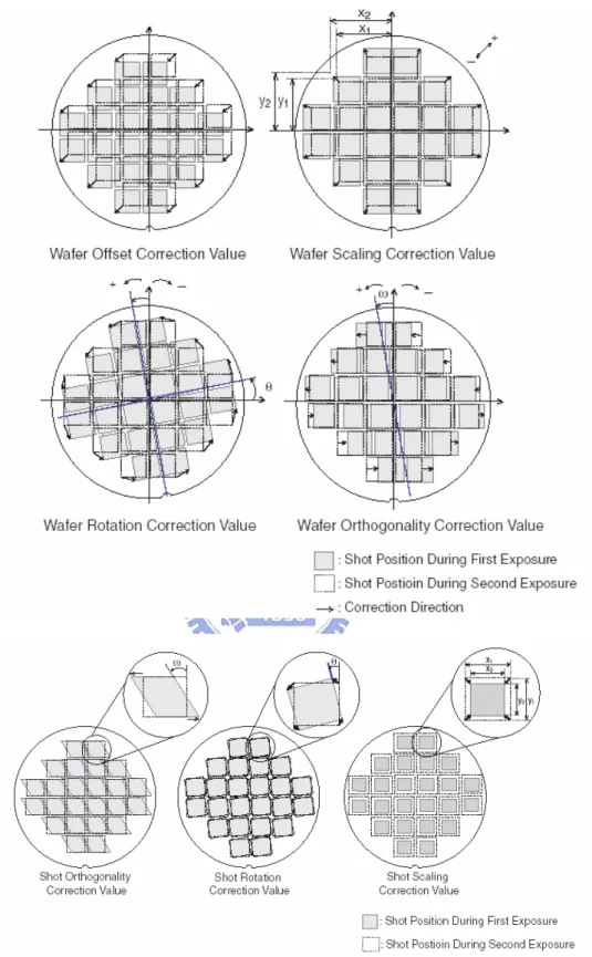
misplacement between the layer and its previous layer is called overlay error, which can be measured by overlay metrology tool. The measured results can be separated to some linear items; those linear items (overlay offset) can be compensated to adjust the alignment offset of exposure tool for minimizing the overlay error.
2.1.1 Definition
Here, we list the main definition for some terms.
Overlay Error: The pattern misplacement between the layer and its previous layer,
which can be measured by overlay metrology tool.
Alignment Offset: The compensated valve of each linear item is used to minimize the
overlay error for scanner alignment system.
Overlay Offset (Figure 2-1): The linear items, calculated by overlay error, can be used
for adjusting the alignment offset of exposure tool for minimizing the overlay error. Those linear items in step and scan lithography system includes: Wafer Offset X, Wafer Offset Y, Wafer Scaling X, Wafer Scaling Y, Wafer Rotation, Wafer Orthogonal, Shot Scaling X, Shot Scaling Y, Shot Rotation, and Shot Orthogonal.
Overlay Baseline: The sum of alignment offset and overlay offset, in terms of each
4
-2.2 CMP basics [8]:
Lithography process window is very sensitive to the underlying layer topography. The CMP process can provide a very flat surface which provides wider DOF (depth of focus) and a higher resolution of lithography process window.
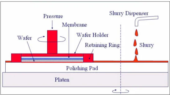
Chemical mechanical polishing (CMP) is a removal process. It strips part of the deposited films by the combination of chemical reaction and mechanical polishing, thus makes the surface smoother and more planarized. A CMP system (Figure 2-2) consists of a polishing pad affixed on a platen, a rotating wafer carrier that holds the wafer face down against the polishing pad, and a slurry dispenser unit. The water-based polishing slurries with abrasive particles and chemical additives are commonly used in CMP process. Slurry is dispensed onto the polishing pad surface, and the front of wafer is pressed downward against the polishing pad. Both the platen and the wafer carrier rotate usually in the same direction. The combined effect of mechanical abrasion and chemical etch removes material from the wafer surface. The built up areas get more mechanical abrasion and are removed faster than recessed areas, that help to planarize the wafer surface.
CMP process helps to planarize the wafer surface, it also introduces some new defects, such as erosion and dishing (Figure 2-3). Erosion is mainly caused by the pattern
density-induced film removal selectivity degradation. The dishing effect usually happens at a larger open area. In W-CMP, the erosion in such way that the oxide in high pattern density area is polished away resulting that the surface sinks below surrounding surface. W in the oxide trench also dishes below the oxide surface.The Erosion and the dishing effect all influence the alignment mark shape, and then impact the alignment accuracy and the overlay error performance.
2.3 Background
Description:
For manufacture capacity and flexibility purpose, a second type etcher is needed to implement the 0.11um generation Contact-1 etching step. Because the Metal-1 layer is aligned to the Contact-1 layer, this second type etcher may change the alignment mark shape and then influence Metal-1 alignment accuracy and overlay error, it is the one of important item needed to be verified for implementing the second type etcher. Two cluster systems combined a TEL ACT8 Track inline with a Nikon S204 Scanner were used for Metal-1 lithography step. Nikon S204 (Figure 2-4) scanner is equipped with FIA (Field Image Alignment) system (Figure 2-5) for wafer alignment.
2.3.1 Definition for Abbreviations
Here, we list the main abbreviation for some terms.
C1: Contact-1 layer M1: Metal-1 layer
ET1:Type1 etcher for Contact-1 etching (TEL DRM) ET2:Type2 etcher for Contact-1 etching (AMT SuperE)
PH1:1st set of Nikon S204 scanner for Metal-1 lithography
PH2:2nd set of Nikon S204 scanner for Metal-1 lithography
2.4 Problem Emerge:
When we check the M1 lithography on the qualification lot of wafers after the etching step in ET2 etcher, the alignment and overlay different from ET1 etcher is highlighted. The alignment offset from ET2 wafers to scanner for minimizing the overlay error was different from that of the ET1 wafers. It means that the alignment mark shape of ET2 lot may be
6
-different from that of ET1, therefore, the detected results from scanner alignment system show some bias. In other words, the M1 overlay baseline of ET2 lots is different from that of ET1 lots. It won’t be manufacturing unfriendly if M1 overlay baseline is still stable for ET2 lots. All we need to do is just to separate the M1 exposure recipe and the feedback system for calculating its alignment offset for ET2 lots in M1 lithography.
In order to verify a stable C1 etching yield from ET2, we start to implement the C1 etching process for wafers by ET2, and also set up the M1 exposure recipe and the feedback system separately for ET2 lots so as to make ET1 and ET2 lots alignment offset not interfere each other. Even so, the ET2 lots still show poor overlay performance and high rework rate. From overlay data analysis we found that the large overlay baseline variation is the main reason for poor overlay performance. In other words, each lot needs to send a wafer ahead for overlay measurement to get adjusted alignment offset for other wafers, then we can get acceptable overlay performance and less rework rate.
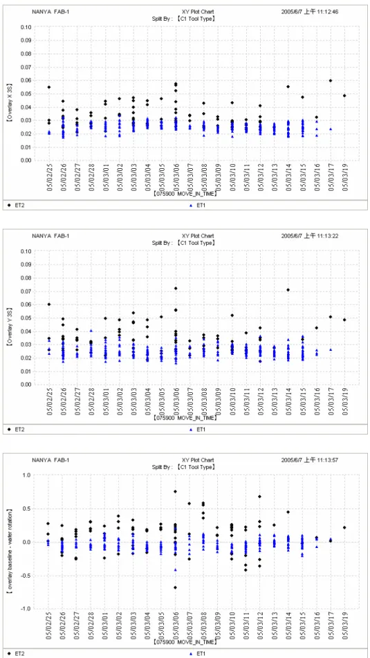
To compare the M1 overlay performance for C1 etching tool ET1 and ET2, the overlay error of ET2 lots is significantly worse than ET1, and the overlay baseline shows a larger variation especially in wafer rotation item for ET2 lots (Figure 2-6).We assume that this abnormal result is attributed to the combination effect from CMP and C1 etching in ET2 tool.
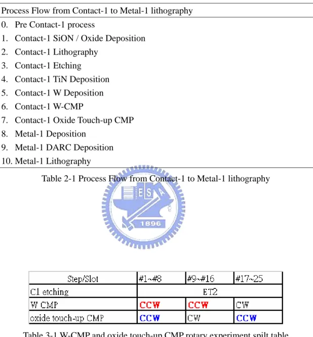
In order to find possible abnormal issues, we study the process flow (Table 2-1) from the film deposition of Contact-1 to the Metal-1 lithography. The variation of alignment mark after the W-CMP and the oxide touch-up CMP may be mainly attributed to the wafer rotation direction. Actually, C1 film deposition, C1 etching, W-CMP, oxide touch-up CMP, and M1 film deposition all possibly affect the alignment mark final shape. From all above, the hypothesis for M1 overlay poor performance on ET2 lots are:
1. The C1 etching process condition in ET2 tool may make the alignment mark shape different from that of ET1 tool.
8
-Chapter 3
Experiment
3.1 Introduction of Experiments Plan
Base on the discussion in Chapter 2, we set up CMP and Etching experiments as follows: CMP experiments:
1. To correlate the W-CMP and oxide touch-up CMP rotary combination to overlay baseline with lots spilt.
2. To correlate W-CMP over polish time to overlay baseline with lot spilt.
3. To correlate oxide touch-up CMP over polish time to overlay baseline with lot spilt.
Etching experiments:
1. By using the cross section SEM to compare the mark difference between ET1 and ET2 C1 etching wafer.
2. To correlate ET2 over etching to overlay baseline with lots spilt.
3.2 CMP Experiments and Results
3.2.1
CMP rotary direction experiments
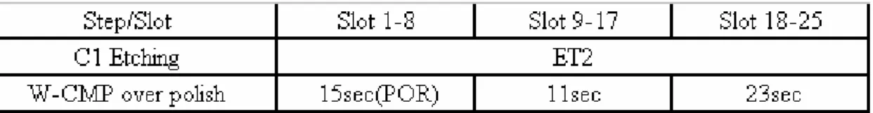
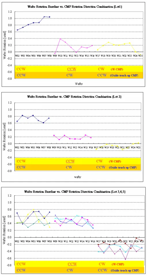
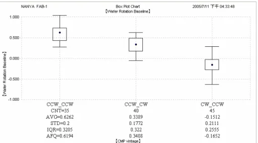
To correlate the W-CMP and oxide touch-up CMP rotary combination to overlay baseline, we prepare 5 lots wafers with same spilt to confirm the repeatability of experimental results. Each lot was spilt into three conditions; the rotary direction combination was CCW/CCW, CCW/CW, and CW/CCW for W-CMP and oxide touch-up CMP, respectively (Table 3-1). The wafer rotation baseline results are shown in Figure 3-1:
spilt 1 as one group and spilt 2/3 as another group. It shows that both two CMP steps affect the wafer rotation baseline.
Lot 2: The distribution of wafer rotation baseline is divided into three groups that match the distribution of three spilt conditions. It shows that both two CMP steps affect the wafer rotation baseline. Furthermore, the effect induced by W-CMP is more significant than that induced by oxide touch-up CMP.
Lot 3/4/5: These three lots show similar results that are quite different from lot 1 and lot2.The overlay offset wafer rotation item become 2 groups, where spilt 1/2 as one group, and split 3 as another group. This result matches with the distribution of W-CMP rotary direction. From these 3 lots, it shows that W-CMP affects wafer rotation baseline but oxide touch-up CMP doesn’t.
Experimental results from these five lots are divided into three groups (Figure 3-2). We conclude as follows:
1. Either W-CMP or oxide touch-up CMP may possibly affect the wafer rotation baseline.
2. Contact-1 etching step is the main factor affecting the overlay baseline and results in the inconsistence between the rotary direction and the overlay baseline.
There are two polish heads for each CMP tool (Figure 3-3), In order to keep the long term leveling of CMP system, the rotary direction of these two polish heads usually is designed in counter direction, respectively, to cancel rotary momentum. In order to avoid the lithography overlay error induced by polish heads interlace on the same CMP system, wafers in the same lot are put on the same polish head of CMP tool. However, from the experimental
10
-results, rotation in counter direction for polish heads on the same CMP system has seriously drifted the overlay baseline. Therefore, it is necessary to keep these two polish heads in same rotary direction to reduce the CMP induced lithography overlay error.
The experimental result of CMP rotary for these five lots are shown in Figure 3-2, the wafer rotation baseline of all wafers ranges around 1.6urad, within the same spilt the range is around 0.6urad. However, this drift is still much higher comparing with ET1 lots that show less than 0.2urad level. To keep the same CMP rotary direction for polish heads is helpful but still not good enough for Metal-1 overlay error control. Because only Contact-1 etching tool is changed during the whole experiment, it is reasonably believed that Contact-1 etching process from ET2 is not optimized. In additional, the subsequent CMP rotary effect further reveals these abnormal results.
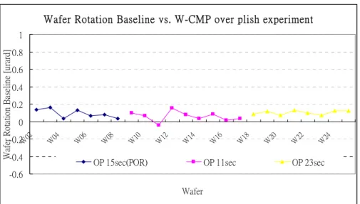
3.2.2 W-CMP Over-Polish Experiments and Results
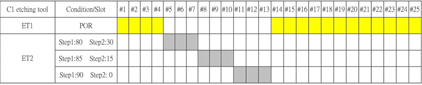
Since the over-polish time may influence the mark shape, we prepare 1 lot wafers for W-CMP process. The overlay baseline vs. the over polish time is listed in Table 3-2. Results are shown in Figure 3-4.
Regular over polish time is 15sec for W-CMP step. However, experimental results show that the over polish time between 11sec to 23sec does not affect the wafer rotation baseline.
3.2.3 Oxide touch-up CMP Over-Polish Experiments and Results
The over-polish time experiment for oxide touch-up CMP is also implemented. We prepare 1 lot wafers for oxide touch-up CMP to correlate the over-polish time with the overlay baseline. The spilt condition is listed in Table 3-3 and the result is shown in Figure 3-5.
to 230A, the wafer rotation baseline slightly changes from 0.6urad to 0.73urad.In addition, as the removal thickness is increased from 350A to 480A, the wafer rotation baseline changes from 0.6 to 0.46urad .We also study the wafer X/Y scaling change for this experiment, as shown in Figure 3-5, the 230A/ 480A spilt wafers are in one group, the mean valve is about 0.2ppm which is lager than 350A spilt wafers. From above results, the oxide touch-up CMP will slightly influence the mean valve of overlay baseline. Regarding the range of those overlay baseline items for each spilt, it is not necessary to change the removal thickness of oxide touch-up CMP.
From Figure 3-5, we also observed the interlacing variation in wafer scaling X and Y baseline. To review Contact-1 to Metal-1 process again (Table 2-1), it is believed that wafers in the same lot deposited with dielectric film or Metal-1 film in interlacing chambers induced the interlacing variation in wafer scaling X and Y baseline. The deposited film thickness also influence lithography overlay control if the overall process integration is not optimized. However, it seems that these interlacing phenomena do not affect the overlay baseline very much. Therefore, we assume that the Contact-1 etching step with different tools plays a major role in the variation of overlay baseline.
3.2.4 The Overlay Performance after Unify CMP Rotary Direction
In order to reveal the main reason causing the variation in overlay baseline, we adjust the rotation of two polish heads in the same direction for each CMP system to eliminate the count direction effect.
After modification in rotation direction, as shown in Figure 3-6, the overlay error and overlay baseline variation range of ET2 lots show some improvement but still not good as ET1 lots does. In order to further identify ET2 etcher induced overlay error and overlay baseline variation, wafers are etched by ET1 or ET2 and subsequently by CMP tool with
12
-count rotation direction or same rotation direction are prepared. In addition, two separate lithography scanner tool is also used to study the overlay performance for each combination. Results are showed in Figure 3-7 and Table 3-4, respectively.
From the results in Figure 3-7 and Table 3-4, we can get following conclusions: 1. The overlay error performance of ET1 lots in PH1 and PH2 scanner shows no difference and is irrelevant to CMP rotation direction.
2. The overlay error performance of ET2 lots is much worse than that of ET1 lots in both PH1 and PH2 scanner where the CMP rotary direction period is not fixed.
3. The overlay error performance and wafer rotation baseline variation of ET2 lots are much improved after the CMP rotary direction is fixed.
4. The overlay error performance of ET2 lots in PH2 scanner is better than that in PH1 under the same CMP rotary direction, and its performance is even close to ET1 lot
remarkable.
5. The overlay error performance of ET2 lots in PH2 scanner is better than that in PH1 scanner where the CMP rotary direction is not fixed. Especially, the variation of wafer rotation baseline is around 2 times larger.
6. The overlay error performance of ET1 lots no overused difference after unifying CMP rotary direction, but the variation of wafer rotation baseline is somewhat improved.
3.2.5 Discussion for Scanner Sensitivity on ET2 etcher lots
This phenomenon really interesting, two scanners didn’t show performance difference in ET1 lots with the same or the count CMP rotary direction, but it show degraded performance difference for ET2 lot with the same or the count CMP rotary direction.
generally knowing as:
(A) TIS (Tool Induced Shift):
This error is attributable to FIA mainly in 2 ways: --The COMA aberration in the FIA Microscope and/or
--The Aperture stop eccentricity for optical axis in the FIA microscope.
(B) WIS (wafer Induced Shift):
This error is attributable to the deformation of alignment marks on the wafer. These deformations may be different in each shot or wafer or lot.
(C) Interaction between TIS and WIS (TISxWIS). It is not possible to eliminate this error. The reduction of TIS and WIS, respectively, can significantly reduce this error and have it become negligible.
In this study, ET2 lots show worse mark deformation and then make their WIS be worse than ET1 lots. TIS of PH1 scanner may be worse than that of PH2 scanner, then further make TIS and TISxWIS of PH1 scanner be worse than those of PH2 scanner. Therefore, the overlay performance becomes worse than that of PH2 scanner for ET2 lots. For ET1 lots, its WIS is better than that of ET2 lots, although the TIS of PH1 scanner is worse than that of PH2
scanner. Obviously, the TIS and TISxWIS are not large enough to make PH1 and PH2 scanner show overlay performance difference.
Both TIS and WIS are needed to be improved, but it is difficult to reduce the TIS of alignment system. It is necessary to optimize the process to improve WIS of ET2.
14
-3.3 Etching Experiments and Results
3.3.1 Alignment Mark cross section SEM study
The overlay performance of ET2 lots is not good as that of ET1 lots. In order to check the alignment mark, cross-section SEM is applied. The alignment mark obtained from cross-section SEM analysis for ET1 and ET2 is shown inFigure 3-8.
It is shown that the alignment mark depth of ET2 wafers was shallower than that of ET1 wafers around 1000A. This difference induces a larger overlay baseline variation for ET2 wafers because the scanner alignment system is not sensitive enough to detect the wafer deformation properly with shallower alignment marks.
To compare the scanner alignment signal, it also reveals the same information (Figure 3-9). The alignment mark 1 was used for Metal-1 lithography alignment. The alignment signal strength of ET2 was weaker than that of ET1 because the alignment marks of ET2 is
shallower. As we compare these two alignment mark signals (Figure 3-10), we find that the signal strength of ET2 is weaker than that of ET1 for smaller features.
To increase the ET2 over-etching time for Contact-1 etching can make alignment mark become deeper and then improve the Metal-1 overlay for ET2 lots.
3.3.2 ET2 Etcher Over-Etching Experiments and Results
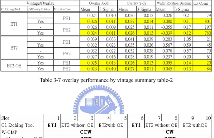
From the cross-section SEM result in Figure 3-8, we prepare two lots of wafers with proper over etching in ET2 etcher to get the same alignment mark depth of ET1, then check the correlation with overlay baseline, yield qualification, and electrical characterization.
both two lots have same total 4 split conditions. The control group is processed in ET1 and the other three experimental groups are processed in ET2 with different etching time. The etching time for all three experimental conditions is designed to get same etching depth as ET1 does. The etching recipe of ET2 is a two step etching process with different gases and pressures. To increase the over-etching time of step 1 etching (Oxide etching) or step 2 etching (SiON etching) can both get deeper alignment mark depth. We prepare three different conditions to get same depth as ET1 does.
Three experimental conditions in ET2 are
Step1:80sec/ Step2:30sec, Step1:85sec/Step2:15sec, and Step1:90sec/Step2:0sec. The original etching condition of ET2 was
Step1:68sec/Step2:30sec.
The overlay baseline result of over-etching experiments are shown in Figure 3-11 and Figure 3-12, it shows that the overlay baseline of all three experimental splits is really closed to that of control spilt. It means that three experimental conditions can make mark depth be similar to that of ET1 wafers. From experimental results we can expect that over-etching can further improve the overlay performance under the same CMP rotary direction.
3.3.3 The Overlay Performance after Implement over etching on
ET2
After this 2 lots pass the yield qualification and electrical characterizations, we set up step 1 etching:80sec ⁄ step 2 etching:30sec as the new condition for ET2 C1 etching and then start release lots to trace M1 overlay performance. Where the CMP rotary direction is fixed. The overlay performance with the new ET2 recipe is shown in Fig 3-13 and Table 3-7. We can get following conclusions:
16
-1. The overlay performance and the variation of wafer rotation baseline for ET2 lots with over etching have been further improved. Where the CMP rotary direction is fixed.
2. The overlay performance and the variation of wafer rotation baseline for ET2 lots with over etching are similar to those of ET1 lot.
3. The overlay performance and the variation of wafer rotation baseline for ET2 lots with a new over etching recipe show no difference on PH1 and PH2 scanner.
After Contact-1 over etching recipe on ET2 etcher is applied, the overlay performance of ET2 lots is as good as ET1 etcher lots.
3.4 CMP v.s. Etching Interaction Experiments and Results
3.4.1 Discussion for CMP v.s. Etching Interaction on ET2 lot
In this study, it was found that the overlay performance of ET2 lots is not as good as ET1 lots. Therefore, we fix the CMP rotary direction and increase the over etching of ET2 etcher to solve ET2 etcher induced problems. It also shows that CMP rotation direction does not affect the overlay performance for ET1 etcher lots,
therefore, it is believed that to make ET2 lots get proper alignment mark depth by over etching is more important than to fix the CMP rotary direction.
3.4.2 Experiments and Results for CMP v.s. Etching Interaction of ET2 lot
In order to prove above assumption, we prepare some wafers with different combination of W-CMP and oxide touch-up CMP rotary direction and then implement Contact-1 etching in
either ET1 or ET2 with over etching recipe or without over-etching recipe to check the effects induced by CMP rotary direction and over etching on overlay control. The detail spilt table is listed in Table 3-8 and the result is shown in Fig 3-14.
The wafer rotation baseline for this experiment is as follows:
1. The wafer rotation baseline for slot 1 and slot 6 are very similar. It means that ET1 wafers is not sensitive to CMP rotary direction. It matches with the previous result that before we implement ET2 etcher for Contact-1 etching in production line.
2. The wafer rotation baseline for slot 4,5,9, and 10 are very close to slot 1 and slot6. It means that ET2 wafers with over etching show deeper alignment mark depth, therefore, not sensitive to CMP rotary direction.
3. ET2 wafers without over etching are very sensitive to CMP rotary direction. The wafer rotation baseline for slot2/3 and slot 7/8 are similar to results from spilt 1 and split 3 in
pervious W-CMP and oxide touch-up CMP rotary direction experiment.
The experimental results have proved the assumption that Contact-1 etching step dominates the poor overlay performance. If the alignment mark is not deep enough, CMP rotary direction will enhance the overlay baseline variation and induce a worse result.
18
-Chapter 4
Conclusion and Discussion
4.1 Conclusion of Experiments:
In this thesis, we discuss the CMP and the etching conditions induced lithography overlay error. Some important conclusions are summarized as follows
(a) Alignment mark depth is the most important factor influencing the overlay error. If the alignment mark depth is too shallow, the scanner alignment system either can not detect enough signal and then induce the alignment fail, or the alignment result can not well correspond to the wafer deformation and then make the overlay baseline variation too big.
(b) CMP process also plays an important role in overlay control. Especially in the condition of alignment mark not deep enough, the CMP rotary direction significantly influences the overlay baseline variation.
(c) In the condition of shallow alignment mark depth, scanner alignment system induced performance difference will become significant.
4.2 The discussion for alignment and overlay strategy:
In general, we separate the factors influence the alignment accuracy and the overlay error performance into 2 parts:
(A) Wafer Process:Including all wafer process that may influence the mark shape. Film deposition thickness, etching time, and CMP polish time, all possibly influence the step height of alignment mark. CMP rotary direction, erosions and dishing effect, etching uniformity, film deposition uniformity all possibly influence the alignment mark deformation and asymmetry. In this study, we increase the etching time and fix the CMP rotary direction to improve the overlay error performance. But in some cases, the optimal process condition for alignment
mark may not be suitable for the features at circuit areas. Most common case is the alignment mark depth being too shallow. Therefore, it is necessary to coat photoresist to protect circuit area and use additional lithography and etching step to increase the alignment mark depth.
(B) Exposure tool alignment system and alignment mark:The hardware of exposure tool alignment system and the algorithm influence the alignment sensitivity of different alignment mark designs, and also the alignment mark step height and the deformation by wafer process affect the alignment sensitivity. The strategies are developed in lithography alignment technology to reduce the effect induced by wafer process and alignment mark in alignment sensitivity.
It includes
--- To use different wavelength for alignment light source. --- To capture more high order alignment signal [2][12].
--- To optimize the algorithm to enhance the signal strength or the signal to noise ratio [9]. --- To optimize the algorithm to correlate the asymmetry signal [10][11].
In addition, the different type and the different dimension of alignment mark have different correlation with alignment algorithm. To evaluate a suitable alignment mark and algorithm combination is very important for better overlay control.
In advanced IC fabrication, lithography is no longer the only factor resulting in the misalignment, Wafer process optimizations and alignment system improvement both important for good overlay control.
20
-Reference
[01] C.P. Alex Chen, Brain Huang, Wilson Lee, W.J. Chung, T.K. Hou, “Chemical Mechanical Planarization Process Induced Within Lot Overlay Variation in 0.2um DRAM: Solution and Simulation Model”, SPIE Vol. 4344, pp 89-97, 2001.
[02] Yuanting Cui, Albert So, Sean Louks, “Fine Tune W-CMP Process with Alignment Mark Selection for Optimal Metal Layer Overlay and Yield Benefits”, SPIE Vol. 5375, pp827-838, 2004.
[03] Igor Jekauc, Bill Roberts, Paul Young, Paul Jowett, Reuben Ferguson, Sean Louks, “Necessary Non-zero Lithography Overlay Correctables for Improved Device Performance for 110nm Generation and Lower Geometries”, SPIE Vol. 5378, pp228-236, 2004.
[04] Christopher J. Gould, Yuanting Cui, Sean Louks ,“Advanced process control applied to metal layer overlay process”, SPIE Vol. 5378, pp28-37, 2004.
[05] Chun-Yen Huang, Boris Habets, Hans-Georg Froehlich, “Alignment improvement for sub 70nm DRAM technology”, 2nd NTC Technical Paper Collection, pp 59-62, 2004. [06] Ai-Yi Lee, Chun-Yen Huang, Chung-Hsin Lin, “Improvement of Overlay Control on
Metal Layer”, 2nd NTC Technical Paper Collection, pp73-76, 2004.
[07] Chi-Long Chung, Hsu-Cheng Fan, “The Investigation of Wafer Bow for sub-0.09um DRAM Technology in 300mm Fab”, 2nd NTC Technical Paper Collection, pp260-264, 2004.
[08] Hong Xiao, “Introduction to Semiconductor Manufacturing Technology”,pp505-544, 2001.
[09] Tadashi Nagayama, Shinichi Nakajima, Ayako Sugaya, Yuho Kanaya, Ayako Sukegawa “New Method to Reduce Alignment Error Caused by Optical System”, SPIE Vol. 5038,
pp849-860, 2003.
[10] Ayako Sugaya, Yuho Kanaya, Shinishi Nakajima, Tadashi Nagayama, Naomasa Shiraishi “Innovative Optical Alignment Technique for CMP Wafers ”, SPIE Vol. 4691, pp959-970, 2002.
[11] Shinishi Nakajima, Yuho Kanaya, Akira Takahashi, Shinishi, Koji Yoshida, Hideo Mizutani, “Improving the Measurement Algorithm for Alignment ”, SPIE Vol. 4344, pp572-582, 2001.
[12] Jeroen Huijbregtes, Richard van Harren, Andre Jeunink, Paul Hinnen, Bart Swinnen, Ramon Navarro, Geert Simons, Frank van Bilsen, Hoite Tolsma, Henry Megens “Overlay Performance with Advanced ATHENA Alignment Strategies”, SPIE Vol. 5038, pp918-928, 2003.
[13] Hideki. Ina, Takahiro Matsumoto, Koichi Sentoku, Katsuhiro Matsuyama, Kazuhiko Katagiri, “New criterion about the topography of W-CMP wafer’s alignment mark”, SPIE Vol. 5038, pp445-452, 2003.
[14] Koichi Sentoku, Takahiro Matsumoto and Hideki Ina, “Novel Strategy for Wafer Induced Shift(WIS)”, SPIE Vol. 4691, pp981-989, 2002.
Process Flow from Contact-1 to Metal-1 lithography 0. Pre Contact-1 process
1. Contact-1 SiON / Oxide Deposition 2. Contact-1 Lithography
3. Contact-1 Etching
4. Contact-1 TiN Deposition 5. Contact-1 W Deposition 6. Contact-1 W-CMP
7. Contact-1 Oxide Touch-up CMP 8. Metal-1 Deposition
9. Metal-1 DARC Deposition 10. Metal-1 Lithography
Table 2-1 Process Flow from Contact-1 to Metal-1 lithography
Table 3-1 W-CMP and oxide touch-up CMP rotary experiment spilt table
-Table 3-2 W-CMP over polish experiment spilt table
Table 3-3 Oxide touch-up CMP over polish experiment spilt table
Lot Count
C1 Etching Tool CMP unify Rotation M1 Litho Tool Mean 3-Sigma Mean 3-Sigma Mean 3-Sigma
- 0.024 0.010 0.026 0.012 0.026 0.21 79 Yes 0.026 0.009 0.026 0.011 0.076 0.11 420 - 0.026 0.009 0.025 0.011 -0.055 0.17 197 Yes 0.025 0.012 0.025 0.014 -0.044 0.11 351 - 0.039 0.033 0.041 0.039 0.203 1.05 21 Yes 0.032 0.023 0.035 0.026 0.567 0.59 45 - 0.032 0.022 0.032 0.028 0.078 0.57 79 Yes 0.027 0.016 0.028 0.019 0.237 0.20 61 ET1 PH1 PH2 ET2 PH1 PH2
Vintage/Overlay Overlay X-3S Overlay Y-3S Wafer Rotation Baseline
24
-C1 etching tool Condition/Slot #1 #2 #3 #4 #5 #6 #7 #8 #9 #10 #11 #12 #13 #14 #15 #16 #17 #18 #19 #20 #21 #22 #23 #24 #25
ET1 POR
Step1:80 Step2:30 Step1:85 Step2:15 ET2
Step1:90 Step2: 0
Table 3-5 C1 over etching experiment spilt table-Lot1
C1 etching tool Condition/Slot #1 #2 #3 #4 #5 #6 #7 #8 #9 #10 #11 #12 #13 #14 #15 #16 #17 #18 #19 #20 #21 #22 #23 #24 #25
ET1 POR
Step1:80 Step2:30 Step1:85 Step2:15 ET2
Step1:90 Step2: 0
Lot Count
C1 Etching Tool CMP unify Rotation M1 Litho Tool Mean 3-Sigma Mean 3-Sigma Mean 3-Sigma
- 0.024 0.010 0.026 0.012 0.026 0.21 79 Yes 0.026 0.011 0.027 0.014 0.080 0.11 801 - 0.026 0.009 0.025 0.011 -0.055 0.17 197 Yes 0.024 0.011 0.026 0.013 -0.039 0.12 780 - 0.039 0.033 0.041 0.039 0.203 1.05 21 Yes 0.032 0.023 0.035 0.026 0.567 0.59 45 - 0.032 0.022 0.032 0.028 0.078 0.57 79 Yes 0.027 0.016 0.028 0.019 0.237 0.20 61 Yes PH1 0.025 0.013 0.026 0.013 0.095 0.14 20 Yes PH2 0.023 0.010 0.027 0.011 0.045 0.13 84 ET1 PH1 PH2 ET2 PH1 PH2 ET2-OE
Vintage/Overlay Overlay X-3S Overlay Y-3S Wafer Rotation Baseline
Table 3-7 overlay performance by vintage summary table-2
Table 3-8 CMP rotary direction v.s. etching interaction on overlay baseline wafer rotation experiment spilt table
Figure 2-1 Schematic of overlay offset linear items
-Figure 2-2 Schematic of a CMP system
Key Components of Nikon Scanner System (1) Illumination System
28
-Figure 2-4 Schematic of Nikon Scanner System (2) Reticle Alignment System (3) Reticle
(4) Reticle Stage (5) Projection Lens
(6) Wafer alignment System ‘FIA’ (7) Wafer
(8) Wafer Stage
Light travels through (a) Lamp Unit (b) Optical Fiber and (c) Illumination Optics, falling on (d) Half Prism. The Half Prism reflects the light onto the wafer through (e) the Objective Lens, illuminating (f) the Alignment Mark on the wafer. The Alignment Mark thus illuminated is captured by (i) the CCD’ Cameras through (g) the FIA Microscope. The CCD’ Camera then transmits electronically this image signal to (j) the Image Processing Unit (IPU). The IPU automatically measured the image position on the CCD which ultimately is the wafer alignment position
Figure 3-1 the wafer rotation baseline result of W-CMP and touch-up CMP experiment
-Figure 3-2 the wafer rotation baseline result summary of W-CMP and touch-up CMP experiment
1
2
Wafer Rotation Baseline vs. W-CMP over plish experiment -0.6 -0.4 -0.2 0 0.2 0.4 0.6 0.8 1 W02 W04 W06 W08 W10 W12 W14 W16 W18 W20 W22 W24 Wafer W af er R o ta tion B as el ine [ ur ar d]
OP 15sec(POR) OP 11sec OP 23sec
Figure 3-4 W-CMP Over-polish experiment result
-W a fe r R ot a t i on B a se l i ne vs. oxi de t ouc h-up C MP ove r pol i sh -0.6 -0.4 -0.2 0 0.2 0.4 0.6 0.8 1 W02 W03 W04 W05 W06 W07 W08 W09 W10 W11 W12 W13 W14 W15 W16 W17 W18 W19 W20 W21 W22 W23 W24 W25 Wafer W af er R ota tio n B as el in e [ ur ad ]
OP 350A(POR) OP 230A OP 480A
W a fe r S c a l ing X B a se l ine vs. Oxide Touc h-up C MP ove r pol ish
-0.6 -0.4 -0.2 0 0.2 0.4 0.6 W02 W03 W04 W05 W06 W07 W08 W09 W10 W11 W12 W13 W14 W15 W16 W17 W18 W19 W20 W21 W22 W23 W24 W25 Wafer W af er S ca li ng X B as el ine [ ppm ]
OP 350A(POR) OP 230A OP 480A
W a fe r S c a ling Y B a se l ine vs. Oxi de Touc h-up C MP ove r pol ish
-0.6 -0.4 -0.2 0 0.2 0.4 0.6 W02 W03 W04 W05 W06 W07 W08 W09 W10 W11 W12 W13 W14 W15 W16 W17 W18 W19 W20 W21 W22 W23 W24 W25 Wafer W afe r S ca li ng Y B as el in e [p pm ]
OP 350A(POR) OP 230A OP 480A
Unify the CMP rotary direction
Unify the CMP rotary direction
Unify the CMP rotary direction
Figure 3-6 overlay X/Y 3 sigma and overlay baseline wafer rotation before and after unify the CMP rotary direction
-Unify the CMP rotary direction
Unify the CMP rotary direction
Unify the CMP rotary direction
Figure 3-7 Overlay X/Y 3 Sigma and Overlay baseline wafer rotation, before and after unify the CMP rotary direction, by tool and condition vintage
(Alignment mark cross section SEM by ET1 etcher)
(Alignment mark cross section SEM by ET2 etcher)
Figure 3-8 Alignment mark cross section SEM comparison on ET1 and ET2 etchers
-FIA alignment signal of alignment mark 1 by ET2
FIA alignment signal of alignment mark 1 by ET1
FIA alignment signal of alignment mark 2 by ET2
FIA alignment signal of alignment mark 1 by ET1
Figure 3-10 FIA alignment signal of alignment mark 2 comparison on ET1 and ET2 etchers
-Overlay Baseline vs. over-etching Experiment [Wafer X Scaling] -0.6 -0.4 -0.2 0 0.2 0.4 W02 W03 W04 W05 W06 W07 W08 W09 W10 W11 W12 W13 W14 W15 W16W17 W18 W19 W20 W21 W22 W23 W24 W25 Wafer W af er S ca li ng X B as el ine [ ppm ] ET1-Control ET2-Experiment 1 ET2-Experiment 2 ET2-Experiment 3
Overlay Baseline vs. over-etching Experiment [Wafer Scaling Y]
-0.6 -0.4 -0.2 0 0.2 0.4 W02 W03 W04 W05 W06 W07 W08 W09 W10 W11 W12 W13 W14 W15 W16 W17 W18 W19 W20 W21 W22 W23 W24 W25 Wafer W af er S ca ling Y B as el ine [ ppm ] ET1-Control ET2-Experiment 1 ET2-Experiment 2 ET2-Experiment 3
Overlay Baseline vs. over-etching Experiment [Wafer Rotation]
-0.6 -0.4 -0.2 0 0.2 0.4 W02 W03 W04 W05 W06 W07 W08 W09 W10 W11 W12 W13 W14 W15 W16 W17 W18 W19 W20 W21 W22 W23 W24 W25 Wafer W af er R ota tio nB as elin e [ ur ad ] ET1-Control ET2-Experiment 1 ET2-Experiment 2 ET2-Experiment 3
Overlay Baseline vs. over-etching Experiment [Wafer Orthogonal]
-0.6 -0.4 -0.2 0 0.2 0.4 W02 W03 W04 W05 W06 W07 W08 W09 W10 W11 W12 W13 W14 W15 W16 W17 W18 W19 W20 W21 W22 W23 W24 W25 Wafer W af er O rt ho gona l B as el in e [ur ad] ET1-Control ET2-Experiment 1 ET2-Experiment 2 ET2-Experiment 3
Overlay Baseline vs. over-etching Experiment [Wafer Scaling X] -0.6 -0.4 -0.2 0 0.2 0.4 W02 W03 W04 W05 W06 W07 W08 W09 W11 W12 W13 W10 W14 W15 W16 W17 W18 W19W20 W21W22 W23 W24 W25 Wafer W af er S ca lin g X B as elin e [p pm ] ET1-Control ET2-Experiment 1 ET2-Experiment 2 ET2-Experiment 3
Overlay Baseline vs. over-etching Experiment [Wafer Scaling Y]
-0.6 -0.4 -0.2 0 0.2 0.4 W02 W03 W04 W05 W06 W07 W08 W09 W11 W12 W13 W10 W14 W15 W16 W17 W18 W19 W20 W21 W22 W23 W24 W25 Wafer W afe r S ca ling Y B as el in e [ppm ] ET1-Control ET2-Experiment 1 ET2-Experiment 2 ET2-Experiment 3
Overlay Baseline vs. over-etching Experiment [Wafer Rotation]
-0.6 -0.4 -0.2 0 0.2 0.4 W02 W03 W04 W05 W06 W07 W08 W09 W11 W12 W13 W10 W14 W15 W16 W17 W18 W19 W20 W21 W22 W23 W24 W25 Wafer W af er R otatio nB as elin e [ ur ad ] ET1-Control ET2-Experiment 1 ET2-Experiment 2 ET2-Experiment 3
Overlay Baseline vs. over-etching Experiment [Wafer Orthogonal]
-0.6 -0.4 -0.2 0 0.2 0.4 W02 W03 W04 W05 W06 W07 W08 W09 W11 W12 W13 W10 W14 W15 W16 W17 W18 W19 W20 W21 W22 W23 W24 W25 Wafer W af er O rt hogon al B as el in e [u ra d] ET1-Control ET2-Experiment 1 ET2-Experiment 2 ET2-Experiment 3
Figure 3-12 The overlay baseline result of over-etching experiment 1ot 2
-Unify the CMP rotary direction Implement ET2 over etching
Unify the CMP rotary direction Implement ET2 over etching
Unify the CMP rotary direction Implement ET2 over etching
Figure 3-13 Overlay X/Y 3 Sigma and Overlay baseline wafer rotation, unify the CMP rotary direction and before/after ET2 over etching implement, by tool and condition vintage
CMP Rotary diection v.s Etching Interaction for Wafer Rotation Baseline -0.4 -0.2 0 0.2 0.4 0.6 Wafer Wa fe r R ota tio n B as elin e [u ra d] 0.071 0.402 0.478 0.033 0.06 0.001 -0.225 -0.269 -0.084 -0.042 1 2 3 4 5 6 7 8 9 10
Figure 3-14 CMP rotary direction v.s. over etching interaction experiment result