國立交通大學
電子工程學系 電子研究所碩士班
碩士論文
元件圖案相依的金屬誘化側向結晶之複晶矽
薄膜電晶體的製作與特性研究
Fabrication and Characterization of Pattern-Depended
Metal Induced Lateral Crystallization Polysilicon Thin
Film Transistors with Nano Wire Channel
研 究 生: 吳元均
指導教授: 羅正忠教授
元件圖案相依的金屬誘化側向結晶之複晶矽薄膜電晶體
的製作與特性研究
研究生: 吳元均
指導教授: 羅正忠教授
國立交通大學
電子工程學系 電子研究所碩士班
中文摘要
在此論文中,我們首先提出一個以標準四道光罩,所製作之元件
圖案相依的金屬誘化側向結晶之複晶矽薄膜電晶體。根據實驗結果顯
示,由於載子遷移率的提昇以及較佳的閘極控制能力,電晶體的電特
性被大幅的改善。研究中發現,載子遷移率是與元件的通道寬度相
依。對同樣閘極長度為 5 um 的元件而言,遷移率隨著通道寬度的縮
減而增加,這是由於窄通道效應提升了複晶矽晶粒的側向尺寸。此
外,實驗結果也顯示出,對相同十條奈米通道的元件,隨著閘極長度
的下降,載子的遷移率亦隨之提升。這是由於閘極所跨的通道內,存
在較少的複晶矽晶粒邊界缺陷所造成的。此外在短通道元件的研究,
藉由比較單一通道與十條奈米通道的元件,我們發現單一通道的元件
展現出接觸碰穿的現象,然而十條奈米通道的元件,依然保持著良好
的開關特性。此現象可被解釋為,十條奈米通道的元件,由於它的環
繞式閘極的結構,使其有較佳的閘極控制能力來降低橫向電場,以抑
制短通道的效應。此元件圖案相依的,金屬誘化側向結晶之複晶矽薄
膜電晶體的製程,完全相容於目前互補式金氧半(CMOS)場效電晶體的
技術,而且不需要額外的光罩製程。此元件可被運用於高效能的複晶
矽薄膜電晶體積體電路,尤其是在主動式薄膜電晶體液晶顯示器
(AMLCD) ,以及三維立體的金氧半場效電晶體積體電路。
關鍵字:金屬誘化側向結晶,元件圖案相依的金屬誘化側向結晶,遷
移率,短通道效應,複晶矽薄膜電晶體,主動式薄膜電晶體
液晶顯示器。
Fabrication and characterization of pattern-depended
metal induced lateral crystallization polysilicon thin film
transistors with nano wire channel
Student: Yuan-Chun Wu
Advisor: Prof. Jen-Chung Lou
Department of Electronics Engineering and Institute of Electronics
National Chiao Tung Unversity, Hsinchu, Taiwan
Abstract
In this thesis, we firstly develop a new pattern-depended MILC thin film transistors (PDM TFTs) with standard four masks process. The experiment results demonstrate that the electrical properties of PDM TFT’s can be significantly improvement by carrier mobility enhancement and superior gate controllability. Experiment results show that the field effect mobility is highly depended on multi-channel width. For the same gate length L=5um, the field effect mobility increasing with channel number, resulting its polysilicon grain size enhanced by channel width limitation effect. In addition, experiment results also show that at the same ten multiple nano-wire channels, the field effect mobility increasing with gate length decreasing from L = 10 um, L = 5 um, L = 2 um to L = 1 um, resulting its
polysilicon grain boundary defects lowering. Moreover, in short channel effect (L = 1um) study, comparing the single channel and ten multiple nano-wire channels devices. The single channel TFT shows punch-through phenomena. It ca be explain that the ten multiple nano-wire channels TFT has the better gate controllability due to its nano-wires structure behavior than single channel TFT. The lateral electrical field of ten multiple nano-wire channels TFT can be effectively reduced by additional two side-gates control. These PDM TFTs process is compatible with CMOS technology, and involves no any extra mask process. Such PDM TFTs are thus highly promising for use in future high-performance polysilicon TFT applications, especially in AMLCD and 3D MOSFET stacked circuits.
Key words: Metal induced lateral crystallization, Pattern-depended metal induced
lateral crystallization, Mobility, Short channel effect, Polysilicon thin film transistor, AMLCD.
致謝
時光飛逝,轉眼間已過了兩個寒暑,在這兩年的碩士生涯中,首
先要感謝我的指導教授羅正忠博士以及張鼎張博士,由於兩位老師在
研究上給予我細心的指導與教誨,讓我在學術及研究上都有莫大的收
穫,在此對兩位老師致上內心最誠摯的敬意與謝意。
此外,由衷感謝行政院國科會國家奈米元件實驗室的劉柏村博
士,在這些日子以來的指導與協助。同時也感謝工研院能源與資源研
究所金光祖博士、鄭曉芬、張佩琳、陳秋美、徐靜怡,與你們的合作
使我獲益良多。另感謝龔正教授與金光祖博士,在百忙之中撥允參加
口試擔任委員。
由於國家奈米元件實驗室以及交通大學奈米中心提供優良的研
究設備與豐富的資源,以及各位工程師的幫忙及協助下,使得實驗得
以順利進行,在此由衷的感謝你們。
論文的完成,感謝吳永俊學長以及涂峻豪學長在實驗上的照顧與
幫助,此外,冉曉雯學姐、蔡宗鳴學長、陳紀文學長、顏碩廷學長、
陳致宏學長、葉炳宏學長、楊政桓學長、陳世璋學長、王敏全學長、
楊富明學長、陳世青學長、張大山學長…等諸位學長,感謝你們的鼓
勵與協助,在我實驗遇到困難的時候 H與我指正與建議
。同時,也感
謝曾經一起努力的同學們,泩宏、泓緯、稚軒、瓊詒、興華、子軒、
育廷、炳麟、世仰、家榮,和你們一塊打拼的情景歷歷在目;還有感
謝實驗室的學弟妹們適時的幫忙。
最後,感謝我的父母家人多年來辛苦的栽培與教誨,使我在求學
的生涯中在各方面給予支持,使我無後顧之憂,在此獻上內心最深的
謝意。
謹以此文獻給我的老師、家人與好友。
元均 2004
Contents
Chinese Abstract
2
English Abstract
4Acknowledgment
6
Contents
8
Table Captions
10
Figure Captions
11
Chapter 1. Introduction
16
1-1. Introduction
16
1-2. Motivation
18
1-3. Thesis outline
19
Chapter 2. Polysilicon conduction mechanism & MILC formation
mechanism
21
2-1. TFT transportation mechanism
21
2-2. Method of Device Parameter Extraction
24
2-2-1. Determination of the threshold voltage
25
2-2-2. Determination of the subthreshold swing
25
2-2-3. Determination of On/Off Current Ratio
25
2-2-4. Determination of the field-effect mobility
26
2-3. TFT non-ideal effect
27
2-3-1. leakage
27
2-3-2. kink effect
28
2-4. MILC formula mechanism
28
Chapter 3. Device fabrication
38
3-1. Metal induced lateral crystallization test pattern fabrication
3-2. Pattern-depended MILC TFT fabrication
39
Chapter 4. Result and Discussion
47
4-1. Analysis of mobility related to multiple channel numbers
and width effect
47
4-2. Analysis of mobility related to gate length with the same
M10 structure
50
Chapter 5. Conclusions
74
Table captions
Chapter 3
Table 3-1 The MILC length with different heat treatments and seeding window width.
Chapter 4
Table 4-1 Summary all devices dimension. All devices are top single-gate structure. Table 4-2 Device a parameters of M10, M5, M2 and S1. All parameters were
extracted at Vd = 5V, except for the field-effect mobility which were
extracted at Vd = 0.1V.
Table 4-3 Device a parameters of L1M10, L2M10, L5M10 and L10M10. All parameters were extracted at Vd = 5V, except for the field-effect mobilities
Figure captions
Chapter 2
Fig. 2-1 Sketch of the band diagram of the polycrystalline silicon films
Fig. 2-2 A schematic MOSFET cross section, showing the axes of coordinates and the bias voltages at the four terminals for the drain-current model.
Fig. 2-3 Three possible mechanisms of leakage current in polysilicon TFTs, including thermionic emission, thermionic field emission and pure tunneling.
Fig. 2-4 The kink effect in the output characteristics of an n-channel SOI MOSFET. Fig. 2-5 MILC polysilicon formation during annealing process. (a) At the beginning
of the annealing process, many nickel atoms are trapped and nickel silicide is formed at the grain boundaries of the MILC polysilicon region. Those nickel silicide grain boundaries at the MIC to a-Si interfaces, which are reactive regions, are responsible for MILC formation. (b) During the annealing process, the nickel silicide RGB absorbs silicon atoms from the a-Si region and rejects them to the MIC polycrystalline silicon region. As a result, the polysilicon grain grows up in lateral direction.
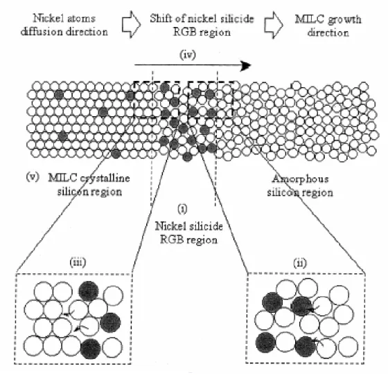
Fig. 2-6 MILC polysilicon formation mechanism. (i) Most of nickel atoms are trapped at the nickel silicide RGB, which is a layer between the amorphous silicon (a-Si) and MILC crystalline silicon regions. (ii) The nickel atoms in the nickel silicide RGB diffuse to the a-Si region and bonds with silicon atoms. The activation energy of the a-Si crystallization is lowered by the nickel impurities. (iii) The silicon atoms are dissociated from the nickel silicide RGB and then bond to the MILC crystalline silicon region. (iv)
Nickel atoms diffuse to the a-Si region and crystallize the a-Si atoms continuously. This leads the shift of nickel silicide RGB and the growth of MILC polysilicon. (v) Only few nickel atoms are left and trapped inside the MILC silicon grain.
Fig. 2-7 Epitaxial silicon growth using nickel silicide, in which, the nickel silicide consumes the a-Si stoms at the leading edge and rejects the Si atoms to the crystalline silicon region.
Chapter 3
Fig. 3-1 MILC Length as a function of heat treatment time.
Fig. 3-2a The optical microscope image of MILC region at 5500C, 48hrs heat treatment.
Fig. 3-2b The SEM image of enlarge area MILC
.
Fig. 3-3a The layout of PDM TFT.
Fig. 3-3b The cross-section view of PDM TFT.
Fig. 3-4a The optical microscope image of finished pattern-depended MILC TFT. Fig. 3-5 The SEM image of active region and MILC window.
Fig. 3-6a The SEM image of MILC region. The average lateral grain size is about 250nm.
Fig. 3-6b The SEM image of multi-channel region. The average lateral grain size is about 250nm.
Chapter 4
Fig. 4-1 (a) Schematic diagram of M10 polysilicon TFT. (b) Cross-section view of Fig. 1a AA’ direction.
(c) One of channel cross-section view of Fig. 1a BB’ direction.
Fig. 4-2 (a) Scanning electron microscopy photography of active pattern with the source, the drain and multiple nano-wire channels of M10 TFT. (b) Magnified area of multiple nano-wire channels. The each nano-wire width is 67 nm.
Fig. 4-3a Device Id-Vg characteristics of L5M10 (L/W = 5um/67nm×10) polysilicon
TFT.
Fig. 4-3b Device Id-Vd characteristics of L5M10 (L/W = 5um/67nm×10) polysilicon
TFT
Fig. 4-4a Device Id-Vg characteristics of L5M5 (L/W = 5um/0.18um×5) polysilicon
TFT.
Fig. 4-4b Device Id-Vd.characteristics of L5M5 (L/W = 5um/0.18um×5) polysilicon
TFT.
Fig. 4-5a Device Id-Vg characteristics of L5M2 (L/W = 5um/0.5um×2) polysilicon
TFT.
Fig. 4-5b Device Id-Vd characteristics of L5M2 (L/W = 5um/0.5um×2) polysilicon
TFT.
Fig. 4-6a Device Id-Vg characteristics of L5S1 (L/W = 5um/1um) polysilicon TFT.
Fig. 4-6b Device Id-Vd characteristics of L5S1 (L/W = 5um/1um) polysilicon TFT.
Fig. 4-7 Field effect mobility (
µ
FE) versus different channel number polysiliconTFTs,with the same gate length L = 5um.
Fig. 4-8 Drain current maximum ON/OFF ratio (R) versus different channel number polysilicon TFTs, with the same gate length L = 5um.
Fig. 4-9 Threshold voltage (Vth) versus different channel number polysilicon TFTs, with the same gate length L = 5um.
Fig. 4-10 Subthreshold slope (SS) versus different channel number polysilicon TFTs, with the same gate length L = 5um.
Fig. 4-11a Schematic plot of PDM M10 TFTs polysilicon grain lateral growth. Fig. 4-11b Schematic plot of PDM S1 TFTs polysilicon grain growth.
Fig. 4-12a Device Id-Vg characteristics of L10M10 (L/W = 10um/0.67um) polysilicon
TFT.
Fig. 4-12b Device Id-Vd characteristics of L10M10 (L/W = 10um/0.67um) polysilicon
TFT.
Fig. 4-13a Device Id-Vg characteristics of L10S1 (L/W = 10um/1um) polysilicon TFT.
Fig. 4-13b Device Id-Vd characteristics of L10S1 (L/W = 10um/1um) polysilicon TFT.
Fig. 4-14a Device Id-Vg characteristics of L2M10 (L/W = 2um/0.67um) polysilicon
TFT.
Fig. 4-14b Device Id-Vd characteristics of L2S1 (L/W = 2um/0.67um) polysilicon
TFT.
Fig. 4-15a Device Id-Vg characteristics of L1S1 (L/W = 2um/1um) polysilicon TFT.
Fig. 4-15b Device Id-Vd characteristics of L1S1 (L/W = 2um/1um) polysilicon TFT.
Fig. 4-16a Device Id-Vg characteristics of L1M10 (L/W = 1um/0.67um) polysilicon
TFT.
Fig. 4-16b Device Id-Vd characteristics of L1M10 (L/W = 1um/0.67um) polysilicon
TFT.
Fig. 4-17a Device Id-Vg characteristics of L1S1 (L/W = 1um/1um) polysilicon TFT.
Fig. 4-17b Device Id-Vd characteristics of L1S1 (L/W = 2um/1um) polysilicon TFT.
Fig. 4-18 Field effect mobility (
µ
FE) versus different channel length polysilicon TFTs.The dots value present average value and error bars present standard deviation.
polysilicon TFTs.
Fig. 4-20 Threshold voltage (Vth) versus different channel number polysilicon TFTs. Fig. 4-21 Subthreshold slope (SS) versus different channel number polysilicon TFTs. Fig. 4-22a Schematic plot of PDM M10 TFTs polysilicon grain lateral growth. Fig. 4-22b Schematic plot of PDM M10 TFTs polysilicon grain lateral growth.
Chapter 1
Introduction
1-1. Overview of polysilicon thin-film transistor technology
In recent years, polycrystalline silicon thin-film transistors (polysilicon TFTs) have drawn much attention because of their widely applications on active matrix liquid crystal displays (AMLCDs) [1], and organic light-emitting displays (OLEDs) [2]. Except large area displays, polysilicon TFTs also have been applied into some memory devices such as dynamic random access memories (DRAMs) [3], static random access memories (SRAMs) [4], electrical programming read only memories (EPROM) [5], electrical erasable programming read only memories (EEPROMs) [6], linear image sensors [7], thermal printer heads [8], photo-detector amplifier [9], scanner [10], neutral networks [10]. Lately, some superior performances of polysilicon TFTs also have been reported by scaling down device dimension or utilizing novel crystallization technologies to enhance polysilicon film quality [11]-[12]. This provides the opportunity of using polysilicon TFTs into three-dimension (3-D) integrated circuit fabrication. Of course, the application in AMLCDs is the primary trend, leading to rapid developing of polysilicon TFT
technology.
The major attraction of applying polycrystalline silicon thin-film transistors (polysilicon TFTs) in active matrix liquid crystal display (AMLCDs) lies in the greatly improved carrier mobility in polysilicon film and the capability of integrating the pixel switching elements and the capability to integrate panel array and peripheral driving circuit on the same substrates [13]-[15]. In polysilicon film, carrier mobility larger than 10 cm2/Vs can be easily achieved, that is enough to used as peripheral driving circuit including n- and p-channel devices. This enables the fabrication of peripheral circuit and TFT array on the same glass substrate, bring the era of system-on-glass (SOG) technology. The process complexity can be greatly simplified to lower the cost. In addition, the mobility of polysilicon TFTs is much better than that of amorphous ones, the dimension of the polysilicon TFTs can be made smaller compared to that of amorphous Si TFTs for high density、high resolution AMLCDs, and the aperture ratio in TFT array can be significantly improved by using polysilicon TFTs as pixel switching elements. This is because that the device channel width can be scaled down while meeting the same pixel driving requirements as in α-Si TFT AMLCDs.
For making high performance poly-crystalline silicon (polysilicon) thin film transistors (TFTs) [16], low-temperature technology is required for the realization of
commercial flat-panel displays (FPD) on inexpensive glass substrate, since the maximum process temperature is limited to less than 6000C. There three major low-temperature amorphous-Si crystallization methods to achieve high performance polysilicon thin film, solid phase crystallization (SPC), excimer laser crystallization (ELC), and Metal-Induced Lateral Crystallization (MILC). MILC technology was initially developed as a low-temperature crystallization technique compared to other low temperature polysilicon technologies such as laser crystallization (LC) [17] or conventional solid-phase crystallization (SPC) [18], MILC is superior because, unlike LC, it is a low-cost batch process and unlike SPC, better quality polysilicon thin film can be obtained [16].
1-2. Motivation
However, most of all previous report of MILC TFTs, additional MILC trench mask process is necessary. In a practical of view, the additional mask will cause the fabrication complexity and decrease the product yield. In addition to this, the application of TFT’s is mainly limited to low-temperature flat-panel display due to its substantially worse performance caused by the grain boundaries in the channel region. It is believed that electrical properties of the TFT’s can be improved if the grain size can be enhanced and the number of grain boundaries in the channel region can be
minimized. It is believed that electrical properties of the TFT’s can be improved if the grain size can be enhanced and the number of grain boundaries in the channel region can be minimized.
To overcome above problems, in this thesis, we firstly develop a new pattern-depended MILC TFTs with standard four masks process. The experiment results demonstrate that the electrical properties of TFT’s can be significantly improvement by carrier mobility enhancement and robust gate controllability.
The crystallization and device fabrication process will be described in chapter 3. And the device characterization will be described in chapter 4. It is found that TFT’s with high mobility and performance can be obtained through the decreasing of the channel width. The influence of grain boundaries on device performance will also be discussed in this chapter. Finally, chapter 5 will give a conclusion on the results obtained.
1-3. Thesis outline
Chapter 1. Introduction
1-4. Overview of polysilicon thin-film transistor technology 1-5. Motivation
Chapter 2. Polysilicon conduction mechanism & MILC formation mechanism 2-1. Transport properties of polycrystalline silicon
2-2. Method of Device Parameter Extraction 2-3. TFT non-ideal effect
2-4. MILC formula mechanism Chapter 3. Experiment
3-1. Metal induced lateral crystallization test pattern fabrication 3-2. Pattern-depended MILC TFT fabrication
Chapter 4. Results and discussion
4-1. Analysis of mobility related to multiple channel numbers and width effect 4-2. Analysis of mobility related to gate length with the same M10 structure 4-3. Analysis of Short channel effect of PDM TFT
Chapter 5. Conclusions References
Chapter 2
Polysilicon conduction mechanism & MILC formation
mechanism
2-1. TFT transportation mechanism
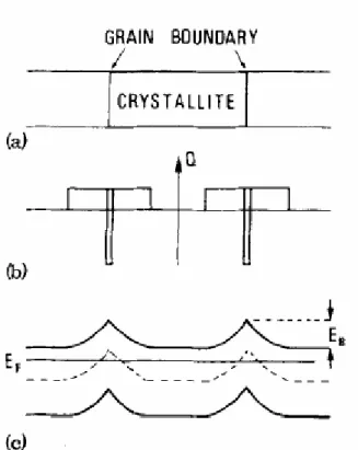
As mentioned in section 1-1 and 1-2, the device characteristics of polysilicon TFTs are strongly influenced by the grain structure in polysilicon film. Even though the inversion channel region is also induced by the gate voltage as in MOSFETs, the existence of grain structure in channel layer bring large differences in carrier transport phenomenon. Many researches studying the electrical properties and the carrier transport in polysilicon TFTs have been reported. A simple grain boundary-trapping model has been described by many authors in details [1]-[3]. In this model, it is assumed that the polysilicon material is composed of a linear chain of identical crystallite having a grain size Lg and the grain boundary trap density Nt. The charge
trapped at grain boundaries is compensated by oppositely charged depletion regions surrounding the grain boundaries. From Poisson’s equation, the charge in the depletion regions causes curvature in the energy bands, leading to potential barriers that impede the movement of any remaining free carriers from one grain to another. When the dopant/carrier density n is small, the polysilicon grains will be fully
depleted. The width of the grain boundary depletion region xd extends to be Lg/2 on
each side of the boundary, and the barrier height VB can be expressed as
s g d s B qnL x qn V ε ε 8 2 2 2 = = (1-1)
As the dopant/carrier concentration is increased, more carriers are trapped at the grain boundary. The curvature of the energy band and the height of potential barrier increase, making carrier transport form one grain to another more difficult. When the dopant/carrier density increases to exceed a critical value N* = Nt / Lg, the polysilicon
grains turn to be partially depleted and excess free carriers start to spear inside the grain region. The depletion width and the barrier height can be expressed as
n N x t d 2 = (1-2) n qN n N qn V s t t s B ε ε (2 ) 8 2 2 2 = = (1-3)
The depletion width and the barrier hight turn to decrease with increasing dopant/carrier density, leading to improved conductivity in carrier transport.
The carrier transport in fully depleted polysilicon film can be described by the thermionic emission over the barrier. Its’ current density can be written as [4]
)] ( exp[ V V kT q qnv J = c − B − (1-4)
where n is the free-carrier density, vc is the collection velocity (vc = kT/2πm∗ ), VB
boundary region. For small applied biases, the applied voltage divided approximately uniformly between the two sides of a grain boundary. Therefore, the barrier in the forward-bias direction decreases by an amount of Vg/2. In the reserve-bias direction,
the barrier increases by the same amount. The current density in these two directions then can be expressed as
1 exp[ ( ] 2 F c B g q J qnv V V kT = − − (1-5) 1 exp[ ( )] 2 R c B g q J qnv V V kT = − + (1-6)
the net current density is then given by ) 2 sinh( ) exp( 2 kT qV kT qV qnv J = c − B g (1-7)
at low applied voltages, the voltage drop across a grain boundary is small compared to the thermal voltage kT/q, Eq. (1.7) then can be simplified as
)] [exp( 2 ) exp( 2 2 kT qV kT V nv q kT qV kT qV qnv J B g c g B c − = − = (1-8) the average conductivity σ = J / Ε = JLg / Vg and the effective mobility µeff = σ / qn
then can be obtained
2 exp( ) c g B q nv L qV kT kT σ = − (1-9) ) exp( ) exp( 0 kT qV kT qV kT L qvc g B B eff = − ≡µ − µ (1-10) where µ0 represents the carrier mobility inside grain regions. It is found that the
conduction in polysilicon is an activated process with activation energy of approximately qVB, which depends on the dopant/carrier concentration and the grain
boundary trap density.
Applying gradual channel approximation to polysilicon TFTs, which assumes that the variation of the electric field in the y-direction (along the channel) is much less than the corresponding variation in the y-direction (perpendicular to the channel), as shown Fig. 2-2. The carrier density n per unit area (cm-2) induced by the gate voltage can be expressed as
( ) ( ) ox G TH y ch C V V V n qt − − = (1.11) . . . y. . D eff dv I J dx dz nq dx dz dy µ =
∫∫
=∫∫
(1.12) 0 0 . . ( ) ch W t y y eff eff ox g th y dV dV dz nqdx W C V V V dy dy µ µ =∫
∫
= − −where tch is the thickness of the inversion layer. Therefore, the drain current ID of
polysilicon TFT then can be given by
)
(
2 0 1 2 L D ff ox g th D D I dy=Wµ C V −V V − V ∫
)
(
1 2 2 D ff ox g th D D W I C V V V V L µ = − − (1-13) Obviously, this I-V characteristic is very similar to that in MOSFETs, except that the mobility is modified.2-2. Methods of device parameter extraction
In this section, we will introduce the methods of typical parameters extraction such as threshold voltage (Vth), subthreshold slope (SS), drain current ON/OFF ratio,
field-effect mobility (µFE).
2-2-1. Determination of the threshold voltage
Many ways are used to determinate the Vth which is the most important parameter of semiconductor devices. In polysilicon TFTs, the method to determinate the threshold voltage is constant drain current method. The gate voltage at a specific drain current IN value is taken as the threshold voltage. This technique is adopted in
most studies of TFTs. Typically, the threshold current IN = ID / (Weff / Leff ) is specified
100 nA for VD = 5V (saturation region) in this thesis.
2-2-2. Determination of the subthreshold slope
Subthreshold slope SS (V/dec.) is a typical parameter to describe the gate control toward channel. The SS should be independent of drain voltage and gate voltage. However, in reality, SS might increase with drain voltage due to short-channel effects such as charge sharing, avalanche multiplication, and punchthrough-like effect. The SS is also related to gate voltage due to undesirable factors such as serial resistance and interface state. In this experiment, the SS is defined as one-half of the gate voltage required to decrease the threshold current by two orders of magnitude (from 10-8A to 10-10A).
2-2-3. Determination of On/Off Current Ratio
represents not only large turn-on current but also small off current (leakage current). It affects gray levels (the bright to dark state number) of TFT AMLCD directly.
There are many methods to specify the on and off current. The practical one is to define the maximum current as on current and the minimum leakage current as off current while drain voltage is applied at 5V.
2-2-4. Determination of the field-effect mobility
The field-effect mobility (µFE) is determined from the transconductance (gm) at
low drain voltage (Vd = 0.1V). The transfer I-V characteristics of polysilicon TFT can be expressed as ] 2 1 ) [( G TH D D2 ox FE D V V V V L W C I =µ − − (3-1) where
Cox is the gate oxide capacitance per unit area,
W is channel width,
L is channel length,
VTH is the threshold voltage.
If VD is much smaller than VG-VTH ( i.e. VD << VG-VTH ) and VG > VTH, the drain
D TH G ox FE D V V V L W C I =µ ( − ) (3-2)
The transconductance is defined as
D FE ox const V G D m V L WC V I g D µ = ∂ ∂ = = . (3-3)
Therefore, the field-effect mobility can be obtained by gm D ox FE WV C L = µ (3-4)
2-3. TFT non-ideal effect
There are two major non-ideal effects will limit the TFTs application, including leakage current, kink-effect. The mechanism of these three non-ideal effects is described briefly as bellow.
2-3-1. Leakage current
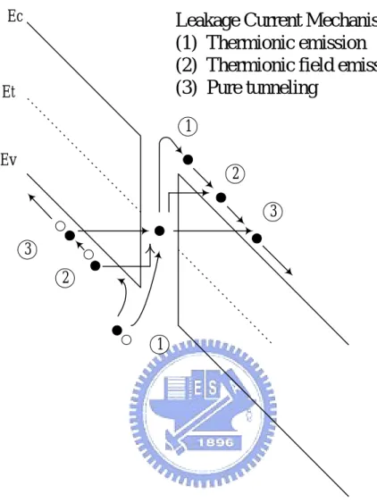
In AMLCD, TFTs play a switching device to turn ON/OFF the current path for charging/discharging the liquid crystal capacitor. Thus, the leakage current should be low enough to remain a pixel gray level before it must be refreshed. The leakage current mechanism in polysilicon has been studied by Olasupe [5]. The leakage current resulted from carrier generation from the polysilicon grain boundary defects. There are three major leakage mechanisms, as shown in Fig. 2-3. The dominant mechanism is a function of the prevailing drain bias. They pointed out carrier
generation from grain boundary defects via thermionic emission and thermionic field emission to be prevalent at a low and medium drain biases, and carrier pure tunneling from polysilicon grain boundary defects to be the dominant mechanism at higher drain bias.
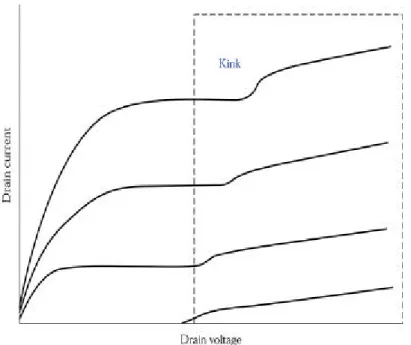
2-3-2. Kink effect [6]
During devices operation, a high field near the drain could induce impact ionization there. Majority carriers, holes in the p-substrate for an n-channel polysilicon TFTs, generated by impact ionization will be stored in the substrate, since there is no substrate contact to drain away these charges. Therefore the substrate potential will be changed and will result in a reduction of the threshold voltage. This, in turn, may cause an increase or a kink in the current-voltage characteristics. The kink phenomenon is shown in Fig. 2-4. This float-body or kink effect is especially dramatic for n-channel devices, because of the higher impact-ionization rate of electrons. The kink effect can be reduced in TFTs by lowering lateral field inside the channel.
2-4. MILC formula mechanism
[7]-[8]In the last few years, several articles have been devoted to study of the growth mechanism of metal-induced-lateral-crystallization (MILC). Earlier observation of Ni
induced crystallization of a-Si revealed that the onset temperature for crystallization of a-Si was significantly reduced in presence of NiSi2 precipitates and crystallization
occurred at around 5000C. The NiSi2 precipitates acts as a good nucleus of Si, which
has similar crystalline structure (the fluorite type, CaF2) and a small lattice mismatch
of 0.4% with Si. In the case of Ni induced crystallization, the growth of crystallites depends strongly on the migration of NiSi2 precipitates, and the driving force for the
migration of NiSi2 precipitates is the reduction in free energy associated with the
transformation of metastable a-Si to stable c-Si.
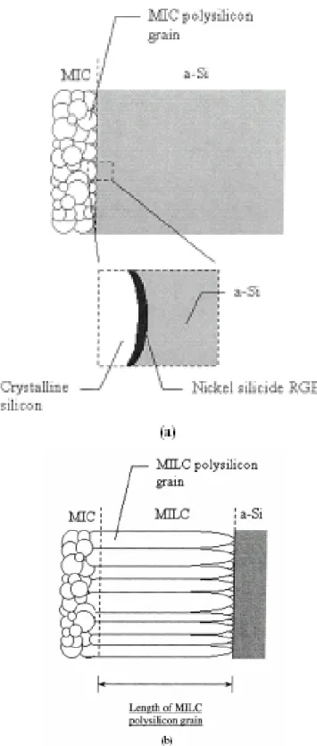
In the MILC process, nickel deposited onto the seed window first reacts with silicon to form a thin nickel silcide film which reduces the activation energy for a-Si crystallization. Thus, a-Si under the silicide is thermally crystallized into polysilicon, and this is called the initial nucleation of crystalline Si on nickel silicide. As this polysilicon is formed by a direct metal induced method, it is also referred as metal-induced-crystallization (MIC) polysilicon. There are many grain boundaries inside the MIC polysilicon layer and these grain boundaries provide good locations for trapping the metal atoms. Due to the fast nickel diffusion in crystalline silicon structure and good nickel trapping property at the crystalline silicon to a-Si interface, most of nickel atoms in the MIC region diffuse to and are trapped at the grain boundaries. The trapped metal atoms react with silicon atoms to form thin layers of
nickel silicide at the grain boundaries. At the MIC to a-Si interface, the nickel silicide at grain boundaries exist as a continuous sandwich layer between MIC polysilicon and a-Si as illustrated in Fig. 2-5a and Fig. 2-5b This continuous nickel silicide layer is a reactive layer, which will be responsible for the grain growth, so it is called nickel silicide reactive grain boundary (RGB). The nickel silicide RGB propagates toward the a-Si region during MILC annealing and a-Si will then be crystallized.
The nickel concentration at the RGB is higher than the neighboring a-Si. Continuous annealing after MIC leads metal atom diffusion to the a-Si layer in lateral directions. Once the nickel atoms are pushed toward the a-Si region, those atoms repair the intrinsic traps and form a new nickel silicide RGB. The nickel atoms lower the activation energy of a-Si crystallization and construct the silicon atoms into a crystalline structure. Since the nickel diffusion in crystalline silicon region is relatively faster, the nickel atoms in the polysilicon region then diffuse to the new silicon grain boundary quickly. This increases the nickel concentration at the RGB and subsequently pushes the nickel atoms to the a-Si again and again. As a result, the a-Si is crystallized to polysilicon in the lateral direction, and this polysilicon is called metal-induced-lateral-crystallization (MILC) polysilicon. As the MILC formation is led by the propagation of the nickel silicide RGB, the MILC polysilicon grains grow along the direction of nickel diffusion. Fig. 2-6 illustrates the silicon crystallization
process during the MILC annealing. The mechanism described does not only explain the polysilicon growth of MILC, but also help to explain the epitaxial silicon growth mechanism by nickel silicide layer propagation from crystalline silicon toward a-Si (refer to Fig. 2-7) proposed by other researches. It tells us why the nickel silicide absorbs silicon atoms from the a-Si region and rejects the excess Si atoms to the crystalline silicon area during epitaxial silicon growth.
Fig. 2-1 Sketch of the band diagram of the polycrystalline silicon films.
W
Chapter 1.0
Gate oxide
Gate
x
y
z
Drain
N+
Source N+
Vd
Vg
t
Fig. 2-2 A schematic MOSFET cross section, showing the axes of coordinates and the bias voltages at the four terminals for the drain-current model.
1 2 3 2 1 3 Ec Ev Et
Leakage Current Mechanism
(1) Thermionic emission
(2) Thermionic field emission
(3) Pure tunneling
Fig. 2-3 Three possible mechanisms of leakage current in polysilicon TFTs, including thermionic emission, thermionic field emission and pure tunneling.
Fig. 2-4 The kink effect in the output characteristics of an n-channel SOI MOSFET.
Fig. 2-5 MILC polysilicon formation during annealing process. (a) At the beginning of the annealing process, many nickel atoms are trapped and nickel silicide is formed at the grain boundaries of the MILC polysilicon region. Those nickel silicide grain boundaries at the MIC to a-Si interfaces, which are reactive regions, are responsible for MILC formation. (b) During the annealing process, the nickel silicide RGB absorbs silicon atoms from the a-Si region and rejects them to the MIC polycrystalline silicon region. As a result, the polysilicon grain grows up in
Fig. 2-6 MILC polysilicon formation mechanism. (i) Most of nickel atoms are trapped at the nickel silicide RGB, which is a layer between the amorphous silicon (a-Si) and MILC crystalline silicon regions. (ii) The nickel atoms in the nickel silicide RGB diffuse to the a-Si region and bonds with silicon atoms. The activation energy of the a-Si crystallization is lowered by the nickel impurities. (iii) The silicon atoms are dissociated from the nickel silicide RGB and then bond to the MILC crystalline silicon region. (iv) Nickel atoms diffuse to the a-Si region and crystallize the a-Si atoms continuously. This leads the shift of nickel silicide RGB and the growth of MILC polysilicon. (v) Only few nickel atoms are left and trapped inside the MILC silicon grain.
Fig. 2-7 Epitaxial silicon growth using nickel silicide, in which, the nickel silicide consumes the a-Si stoms at the leading edge and rejects the Si atoms to the crystalline silicon region.
Chapter 3.
Device fabrication
3-1. Metal induced lateral crystallization test pattern fabrication
6-inch p-type single crystal silicon wafers with (100) orientation were used as the starting materials, and coated with 400-nm-thick thermally grown SiO2. Then,
undoped 50 nm-thick amorphous-Si layer were deposited by low-pressure chemical vapor deposition (LPCVD) on buried oxide. An isolation 100nm-thick TEOS oxide was deposited by LPCVD. The MILC trench was patterned by optical lithography and RIE. Then, a thin 10nm-thick Ni was deposited by PVD. Finally, after 5500C annealing, the MILC was formed.
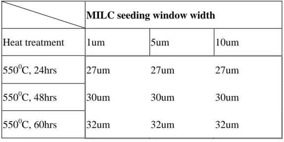
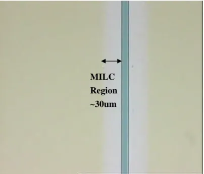
Table3-1 lists the annealing condition of MILC, different heat treatment time and MILC seeding window width. And the results show that MILC length was independent of seeding window width. Figure 3-1 shows that MILC boundary length versus annealing time. From the result, the MILC boundary length is linear depended on annealing time. Figure 3-2a shows optical microscope image of MILC region about 30 um, at 550 0C, 48 hrs. Figure 3-2b shows the SEM image of enlarge area MILC. The a-Si (left) and MILC (right) region are separated clearly, and between them is Ni-rich boundary.
3-2. Pattern-depended MILC TFT fabrication
In this experiment, according previous MILC test sample results, the PDM TFTs device layout with standard four masks is shown in Fig. 3-3a, and the schematic cross sectional view of devices with conventional top-gate structure is shown in Fig. 3-3b.
The fabrication procedure is described as follows.
Step1. Substrate.
6-inch p-type single crystal silicon wafers with (100) orientation were used as the starting materials. After an RCA initial cleaning procedure. Si wafers were coated with 400-nm-thick thermally grown SiO2 in steam oxygen ambient at
1000°C.
Step2. Active region formation (Mask1).
Uundoped 50nm-thick amorphous-Si layer were deposited by low-pressure chemical vapor deposition (LPCVD) on buried oxide by pyrolysis of silane (SiH4)
at 550°C. The active islands (mask1), including source, drain and channel with different dimension were patterned by Electron Beam (Ebeam) lithography and transferred by reactive ion etching (RIE).
Step3. Gate oxide formation
performed to remove the native oxide on the silicon surface. Soon, the gate insulator was deposited in a horizontal furnace using TEOS and O2 gases at
700°C. The thickness of the TEOS oxide thin film is 25nm.
Step4. Gate electrode formation (Mask2)_.
After deposition of gate oxide, 150nm-thick undoped polysilicon films were deposited immediately on the gate oxide by LPCVD at 620°C. The polysilicon layers were patterned by Ebeam lithography and transferred by RIE to define the gate electrode and to be the mask for self-aligned implantation.
Step5. MILC window and contact hole (Mask3) .
After gate formation, a 100nm-thick TEOS oxide layer as passivation layer was deposited by LPCVD. Then, we define the MILC window and contact hole with the same mask (as shown in Fig. 3-3a).
Dopants were activated by rapid thermal annealing (RTA) at 780 ºC for 60 sec.
Step6. Metal induced lateral crystallization
Then, a thin 10nm-thick nickel (Ni) layer was deposited by physical vapor deposition (PVD). The MILC crystallization was carried out at 550°C for 48hrs in an N2 ambient. After long time annealing, the unreacted nickel on passivative
Step7. Self-aligned offset Source/drain formation.
Phosphorus ions at a dose of 5×1015 cm-2 were implanted to form the n+ gate, source/drain regions and the self-aligned offset region were formation in the same process step (as shown in Fig. 3-3b).
Step8. Metallization.
The 300nm-thick aluminum (Al) layer was deposited by physical vapor deposition (PVD) and patterned for source, drain and gate metal pads. Finally, the finished devices were sintered at 400°C for 30 minutes in an N2 ambient.
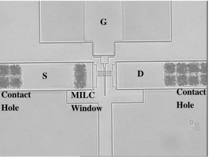
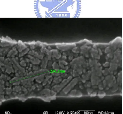
Figure 3-4 shows optical microscope image of finished PDM TFT. Figure 3-5 shows the image of active region and MILC window. Fig. 3-6a shows the SEM image of MILC region. The lateral grain was oriented of initial crystalline structure and the subsequent growth in <111> direction of needlelike crystallites. Fig. 3-6b shows SEM image of multi-channel region. The average lateral grain size is about 250nm.
MILC seeding window width
Heat treatment
1um
5um
10um
550
0C, 24hrs
27um
27um
27um
550
0C, 48hrs
30um
30um
30um
550
0C, 60hrs
32um
32um
32um
Table 3-1. The MILC length with different heat treatments and seeding window width.
20 25 30 35 40 45 50 55 60 65 25 26 27 28 29 30 31 32 33 34 35 Heat treatment:5500C Ni: 10nm
MILC Length (um)
Heat Treatment Time (Hour)
Fig. 3-2a The optical microscope image of MILC region at 5500C, 48hrs heat treatment. MILC Region ~30um
Fig. 3-2b The SEM image of enlarge area MILC
.
Fig. 3-3a The layout of PDM TFT.
Fig. 3-3b The cross-section view of PDM TFT.
CW MILC-W CW Buried oxide
a-Si
Gate
Off-set region ~0.1um 16um MILC window Contact holeSource
Drain
Gate
Fig. 3-4a The optical microscope image of finished pattern-depended MILC TFT.
Fig. 3-5 The SEM image of active region and MILC window.
MILC Window G S D MILC Window Contact Hole Contact Hole S D
Fig. 3-6a The SEM image of MILC region. The average lateral grain size is about 250nm.
Fig. 3-6b The SEM image of multi-channel region. The average lateral grain size is about 250nm.
Chapter 4
Experiment results and discussion
4-1.Analysis of mobility related to multiple channel numbers and
width effect
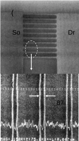
Figure 4-1a shows the device structure of the M10 structure TFT. Fig 4-1b shows the AA’ direction cross-section view of M10 TFT which was a conventional top-gate offset MOSEFET structure. Fig. 4-1c shows the BB’ direction cross-section view of M10 TFT which the channels were surrounded by gate electrode. Table I lists dimension of all proposed PDM polysilicon TFTs. Figure 4-2a presents a after etching investigation (AEI) scanning electron microscopy (SEM) photograph of the polysilicon active region in the TFTs, including the source, the drain and ten multiple nano-wire channels. Figure 4-2b presents a magnified area of multiple nano-wire channels in the TFTs, each width is 67 nm. Figures 4-3 to 4-6 present the electrical characteristics of different channel numbers and width polysilicon TFTs at the same gate length, L = 5um. Each figure (a) of Fig. 4-3 to 4-6 plots a typical transfer curves, and figure (b) plots output curves of polysilicon TFTs. Table 4-2 lists all polysilicon TFT parameters, including field effect mobility (
µ
FE), ON/OFF ratio, threshold (Vth),drain current of Id / (W/L) = 10-7 A at Vd = 5 V. ION is defined of maximum drain turn
on current at Vd = 5V. IOFF is defined drain minimum current at Vd = 5V. Thus,
ON/OFF ratio is defined as ION / IOFF.
For further understanding pattern-depended MILC effect, a serious of device parameters versus different channel width and numbers plot in Fig. 4-7 to Fig. 4-10. Figure 4-7 shows the TFTs
µ
FE versus different channel and width relation. This factindicates that the polysilicon TFTs’ mobility increases from L5S1, L5M5, L5M2 to L5M10. It can be explained that the polysilicon grain size was enhanced by decreasing of channel width. Because that during MILC status, the narrow width will limit the polysilicon grain growth in z-direction. Thus, the polysilicon grain is trend to grow laterally in y-direction. Thus, the polysilicon grain lateral length was enhanced. The mechanism schematic plot of pattern-depended lateral growth is shown in Fig 4-11a. However, for single channel S1 TFT, the polysilicon grains are not entire lateral in y-direction as shown in Fig 4-11b. According to Fig. 3-4a MILC polysilicon grain SEM picture, the lateral grain was oriented of initial crystalline structure and the subsequent growth in <111> direction of needlelike crystallites. Therefore, M10 TFT has lager polysilicon grain size and lower boundaries defects than other TFTs, which is responsible for high
µ
FE. Figure 4-8 shows the TFTs ON/OFF ratio versus differentthe TFTs Vth versus different channel and width relation. All Vth is within 4 to 5. It
should be noted that M10 TFT shows slightly lower other TFTs. It is because that Vth
was extracted by constant value method, and L5M10 TFT has a relatively higher mobility than other TFTs. Figure 10 shows the PDM TFTs subthreshold slope (SS) versus different channel and width relation. SS values are increasing with channel numbers. One may notice that M10 TFT shows smallest SS than others. The steep SS of L5M10 is desirable for the ease of switching the transistor off. The mathematical education of SS could describe as following:
) 1 ( 10 ln ox t C C q kT SS= ⋅ ⋅ + (1) where ox o ox ox t C =ε ⋅ε (2) it Si Si b t qN t qD C = , ⋅ + (3)
Nb,Si is the trap density in the polysilicon layer (cm-3eV-1), Dit is the interface trap
density at the polysilicon/gate oxide dielectirc film (cm-3). Steep SS of M10 can be explained that L5M10 has lower poy-Si grain boundaries to reduce Nb,Si, and achieve
lowest Ct.
On the other hand, in Fig. 3(b) to 6(b), there are showing the light kink-effect for all TFT. It can be explained that the PDM TFTs have self-aligned offset structure (Fig. 3-3b) to reduce the lateral field which is responsible for light kink-effect.
4-2. Analysis of mobility related to gate length with the same M10
structure
In this section, we will discuss the gate length effect of PDM TFTs. Figure 12a presents the Id-Vg transfer curve, and 12b presents the Id-Vd output curve of L10M10
TFT. Figure 13a presents the Id-Vg transfer curve, and 13b presents the Id-Vd output
curve of L10S1 TFT. Figure 14a presents the Id-Vg transfer curve, and 14b presents
the Id-Vd output curve of L2M10 TFT. Figure 15a presents the Id-Vg transfer curve,
and 15b presents the Id-Vd output curve of L2S1 TFT. Figure 16a presents the Id-Vg
transfer curve, and 16b presents the Id-Vd output curve of L1M10 TFT. Figure 17a
presents the Id-Vg transfer curve, and 76b presents the Id-Vd output curve of L1S1 TFT.
For investigating the gate length effect, a serious of device parameters versus different gate length plot in Fig. 4-18 to Fig. 4-21 with the same M10 active region structure. Figure 4-18 shows the TFTs µFE versus different gate length relation. This
fact shows that the polysilicon TFTs’ mobility increases when the gate length decreases. It can be explained that the polysilicon grain boundaries are highly decreasing when gate length is scaling down. For L = 1um, the highest mobility µFE =
72.93 cm2/Vs, results from lowest grain boundaries covered by gate, compared to other TFTs. The schematic plot of gate length L =1 um is shown in Fig 4-22a. However, for L = 10 um TFT, the polysilicon much grain boundaries are covered by long gate length as shown in Fig 4-22b. Figure 4-19 shows the TFTs ON/OFF ratio versus different gate length relation. All TFT has high ON/OFF ratio (>106), except L1M10. Because that the L1M10 has drain induced barrier lowing due to its short gate length. Figure 4-20 shows the TFTs Vth versus different gate length relation. This
subthreshold slope (SS) versus different gate length relation. All SS value is within 0.5 to 0.6.
4-3. Short channel effect of PDM TFT
Considering gate length L = 1 um devices of Fig. 4-16 and Fig. 4-17. For L1S1 TFT, at Vd = 5V, the transfer curve is showing punch-through behavior as shown in Fig. 4-17a. However, in Fig. 4-16a, L1M10 still maintains switch behavior. It can be explained that the thin 50 nm-thick and 67 nm-wide of M10 are fully depleted by tri-gate structure, as shown Fig. 4-1c. It has been reported that the double-gate [1] and gate-all-around SOI MOSFET [2] can reduce the short-channel effects such as DIBL, and subthreshold slope degradation. Therefore, M10 TFT’s tri-gate structure [3] has a better gate controllability, which can resist the lateral field penetration from drain side.
For further understanding the tri-gate effect, the electrical potential and field of TFT (Fig. 4-1a) can be easily explained by the three-dimensional (3D) Poisson equation: 2 V ρ ε ∇ = − (4) y x z A Si eN x y z ξ ξ ξ ε ∂ ∂ + +∂ =− ∂ ∂ ∂ (5)
where is the electrical field in lateral direction. is the depletion charge density.
y A V y eN ξ ρ ∂ = − ∂ = −
y A x y Si eN dy dy y x ξ ξ ξ ε ∂ − ∂ = = − ∂ ∂
∫
∫
(6)For M10 TFT, the lateral electrical field is
y A x z y Si eN dy dy dy y x z ξ ξ ξ ξ ε ∂ − ∂ ∂ = = − − ∂ ∂ ∂
∫
∫
∫
(7)From above equation, the lateral electrical field of M10 TFT is reduced by additional two-side gates control in z-direction (Fig. 4-1c), which is responsible for reduced short channel effect.
Poly
Gate
Gox
Channel
(c).
Fig 4-1. (a) Schematic diagram of M10 polysilicon TFT. (b) Cross-section view of Fig. 1a AA’ direction.
x
z
A
B
B’
A’
x
z
y
(a).
(b).
BOX 4000A
Poly
Gate
Source N
+N
+Drain
Table 4-1 Summary all devices dimension. All devices are top single-gate structure.
Device name Gate length L Channel number Each channel width Effective channel width W L1M10 1um 10 67nm 0.67um
L1S1 1um 1 1um 1um
L2M10 2um 10 67nm 0.67um
L2S1 2um 1 1um 1um
L5M10 5um 10 67nm 0.67um L5M5 5um 5 0.18um 0.9um L5M2 5um 2 0.5um 1um
L5S1 5um 1 1um 1um
L10M10 10um 10 67nm 0.67um L10S1 10um 1 1um 1um
Fig. 4-2 (a) Scanning electron microscopy photography of active pattern with the source, the drain and multiple nano-wire channels of M10 TFT. (b) Magnified area of multiple nano-wire channels. The each nano-wire width is 67 nm.
(
So
Dr
(
Gate voltage (V)
-4 -2 0 2 4 6 8 10
Drain current (A)
10-14 10-13 10-12 10-11 10-10 10-9 10-8 10-7 10-6 10-5 10-4
Field effect mobility ( cm
2 /Vs) 0 20 40 60 80 100 Vd=5V Vd=0.1V L/W=5um/67nm*10 G D S G D S
M10
Fig. 4-3b Device Id-Vd characteristics of L5M10 (L/W = 5um/67nm×10)
polysilicon TFT
Fig. 4-3a Device Id-Vg characteristics of L5M10 (L/W = 5um/67nm×10)
polysilicon TFT.
Drain voltage (V)
0 3 6 9 12 15
Drain current (uA)
0 5 10 15 20 25 Vg=10V Vg=8V Vg=6V L/W=5um/67nm*10
.
Gate voltage (V)
-4 -2 0 2 4 6 8 10
Drain current (A)
10-15 10-14 10-13 10-12 10-11 10-10 10-9 10-8 10-7 10-6 10-5 10-4
Field effect mobility ( cm
2 /Vs) 0 20 40 60 80 100 Vd=5V Vd=0.1V L/W=5um/0.18um*5 G S D G S D
M5
Fig. 4-4b Device Id-Vd.characteristics of L5M5 (L/W = 5um/0.18um×5)
polysilicon TFT.
Fig. 4-4a Device Id-Vg characteristics of L5M5 (L/W = 5um/0.18um×5)
polysilicon TFT.
Drain voltage (V)
0 3 6 9 12 15
Drain current (uA)
0 2 4 6 8 10 12 14 Vg=10V Vg=8V Vg=6V L/W=5um/0.18um*5
Gate voltage (V)
-4 -2 0 2 4 6 8 10
Drain current (A)
10-14 10-13 10-12 10-11 10-10 10-9 10-8 10-7 10-6 10-5 10-4
Field effect mobility ( cm
2 /Vs) 0 20 40 60 80 100 Vd=5V Vd=0.1V L/W=5um/0.5um*2 G S D G S D
M2
Fig. 4-5b Device Id-Vd characteristics of L5M2 (L/W = 5um/0.5um×2)
polysilicon TFT.
Fig. 4-5a Device Id-Vg characteristics of L5M2 (L/W = 5um/0.5um×2)
polysilicon TFT.
Drain voltage (V)
0 3 6 9 12 15
Drain current (uA)
0 2 4 6 8 10 Vg=10V Vg=8V Vg=6V L/W=5um/0.5um*2
Gate voltage (V)
-4 -2 0 2 4 6 8 10
Drain current (A)
10-14 10-13 10-12 10-11 10-10 10-9 10-8 10-7 10-6 10-5 10-4
Field effect mobility ( cm
2 /Vs) 0 20 40 60 80 100 Vd=0.1v Vd=5V L/W=5um/1um G S D G S D
S1
Fig. 4-6a Device Id-Vg characteristics of L5S1 (L/W = 5um/1um)
polysilicon TFT.
Drain voltage (V)
0 3 6 9 12 15
Drain current (uA)
0 2 4 6 8 10 Vg=10V Vg=8V Vg=6V L/W=5um/1um
Fig. 4-6b Device Id-Vd characteristics of L5S1 (L/W = 5um/1um)
Table 4-2 Device a parameters of M10, M5, M2 and S1. All parameters were extracted at Vd = 5V, except for the field-effect mobility which were extracted at Vd =
0.1V.
Device name Mobility (cm2/VS) Vth (V) SS (V/dec.) Ion / Ioff L5M10 42.29 4.05 0.59 2.93 × 10⁶ L5M5 30.62 4.56 0.66 1.87 × 10⁶ L5M2 21.39 4.70 0.78 1.15 × 10⁶ L5S1 18.11 4.79 0.80 2.93 × 10⁶
Fig. 4-7 Field effect mobility (
µ
FE) versus different channel number polysilicon TFTs,with the same gate length L = 5um.
Fig. 4-8 Drain current maximum ON/OFF ratio (R) versus different channel number polysilicon TFTs, with the same gate length L = 5um.
Channel number
M10 M5
M2 S1
Field effect mobility ( cm
2 /Vs) 15 20 25 30 35 40 45 L=5um L=5um Channel number M10 M5 M2 S1 Ion/Ioff (*10 6 ) 0 1 2 3 4 5
Fig. 4-9 Threshold voltage (Vth) versus different channel number polysilicon TFTs, with the same gate length L = 5um.
Fig. 4-10 Subthreshold slope (SS) versus different channel number polysilicon TFTs, with the same gate length L = 5um.
L=5um Channel number M10 M5 M2 S1 Threshold voltage (V) 0 1 2 3 4 5 6 L=5um Channel number M10 M5 M2 S1
Subthreshold swing (V/dec)
0.55 0.60 0.65 0.70 0.75 0.80 0.85
Fig. 4-11a Schematic plot of PDM M10 TFTs polysilicon grain lateral growth. Drain Source MILC window Gate MILC window Drain Source Gate
Gate voltage (V)
-4 -2 0 2 4 6 8 10
Drain current (A)
10-15 10-14 10-13 10-12 10-11 10-10 10-9 10-8 10-7 10-6 10-5 10-4
Field effect mobility ( cm
2 /Vs) 0 20 40 60 80 100 Vd=5V Vd=0.1V L/W=10um/67nm*10
Fig. 4-12a Device Id-Vg characteristics of L10M10 (L/W = 10um/0.67um)
polysilicon TFT.
Drain voltage (V)
0 3 6 9 12 15
Drain current (uA)
0 2 4 6 8 10 12 L/W=10um/67nm*10 Vg=10V Vg=8V Vg=6V
Fig. 4-12b Device Id-Vd characteristics of L10M10 (L/W = 10um/0.67um)
Gate voltage (V)
-4 -2 0 2 4 6 8 10
Drain current (A)
10-14 10-13 10-12 10-11 10-10 10-9 10-8 10-7 10-6 10-5 10-4
Field effect mobility ( cm
2 /Vs) 0 20 40 60 80 100 Vd=0.1V Vd=5V L/W=10um/1um
Fig. 4-13a Device Id-Vg characteristics of L10S1 (L/W = 10um/1um)
polysilicon TFT.
Drain voltage (V)
0 3 6 9 12 15
Drain current (uA)
0.0 0.5 1.0 1.5 2.0 2.5 3.0 Vg=6V Vg=8V Vg=10V L/W=10um/1um
Fig. 4-13b Device Id-Vd characteristics of L10S1 (L/W = 10um/1um)
L/W=2um/67nm*10
Gate voltage (V)
-4 -2 0 2 4 6 8 10
Drain current (A)
10-14 10-13 10-12 10-11 10-10 10-9 10-8 10-7 10-6 10-5 10-4 10-3
Field effect mobility (cm
2 /Vs) 0 20 40 60 80 100 Vd=5V Vd=0.1V
Fig. 4-14a Device Id-Vg characteristics of L2M10 (L/W = 2um/0.67um)
polysilicon TFT.
L/W=2um/67nm*10
Drain voltage (V)
0 3 6 9 12 15
Darin current (uA)
0 20 40 60 80 100 120 140 160 180 Vg=10V Vg=8V Vg=6V
Fig. 4-14b Device Id-Vd characteristics of L2S1 (L/W = 2um/0.67um)
L/W=2um/1um
Gate voltage (V)
-4 -2 0 2 4 6 8 10
Drain current (A)
10-14 10-13 10-12 10-11 10-10 10-9 10-8 10-7 10-6 10-5 10-4 10-3
Field effect mobility (cm
2 /Vs) 0 20 40 60 80 100 Vd=5V Vd=0.1V
Fig. 4-15a Device Id-Vg characteristics of L1S1 (L/W = 2um/1um)
polysilicon TFT.
L/W=2um/1um
Drain voltage (V)
0 3 6 9 12 15
Drain current (uA)
0 20 40 60 80 100 120 Vg=10V Vg=8V Vg=6V
Fig. 4-15b Device Id-Vd characteristics of L1S1 (L/W = 2um/1um)
Gate voltage (V)
-4 -2 0 2 4 6 8 10
Drain current (A)
10-14 10-13 10-12 10-11 10-10 10-9 10-8 10-7 10-6 10-5 10-4 10-3
Field effect mobility ( cm
2 /Vs) 0 20 40 60 80 100 Vg=0.1V Vg=5V L/W=1um/67nm*10
Fig. 4-16a Device Id-Vg characteristics of L1M10 (L/W = 1um/0.67um)
polysilicon TFT.
Drain voltage (V)
0 3 6 9 12 15
Drain current (uA)
0 100 200 300 400 500 Vd=10V Vd=8V Vd=6V L/W=1um/67nm*10
Fig. 4-16b Device Id-Vd characteristics of L1M10 (L/W = 1um/0.67um)
Gate voltage (V)
-4 -2 0 2 4 6 8 10
Drain current (A)
10-11 10-10 10-9 10-8 10-7 10-6 10-5 10-4 10-3
Field effect mobility ( cm
2 /Vs) 0 20 40 60 80 100 Vd=0.1V Vd=5V L/W=1um/1um
Fig. 4-17a Device Id-Vg characteristics of L1S1 (L/W = 1um/1um)
polysilicon TFT.
Fig. 4-17b Device Id-Vd characteristics of L1S1 (L/W = 2um/1um)
polysilicon TFT.
Drain voltage (V)
0 3 6 9 12 15
Drain current (uA)
0 200 400 600 800 Vd=10V Vd=8V Vd=6V L/W=1um/1um
Table 4-3 Device a parameters of L1M10, L2M10, L5M10 and L10M10. All parameters were extracted at Vd = 5V, except for the field-effect mobilities which
were extracted at Vd = 0.1V.
Device name Mobility (cm2/VS) Vth (V) SS (V/dec.) Ion / Ioff L1M10 72.93 1.87 0.60 4.58 × 10⁵ L2M10 64.71 3.16 0.53 4.77 × 10⁶ L5M10 42.29 4.05 0.59 2.93 × 10⁶ L10M10 48.71 3.44 0.55 1.30 × 10⁶
M10
W=67nm*10
Channel length
0 1 2 3 4 5 6 7 8 9 10 11
Field effect mobility ( cm
2 /Vs) 30 40 50 60 70 80 90
Fig. 4-18 Field effect mobility (
µ
FE) versus different channel length polysilicon TFTs.The dots value present average value and error bars present standard deviation.
M10
W=67nm*10
Channel length (um)
0 1 2 3 4 5 6 7 8 9 10 11 Ion/Ioff (X10 6 ) 0 2 4 6 8 10
Fig. 4-19 Drain current maximum ON/OFF ratio (R) versus different channel number polysilicon TFTs.
M10
W=67nm*10
Channel length (um)
0 1 2 3 4 5 6 7 8 9 10 11 Threshold voltage (V) 0 1 2 3 4 5
Fig. 4-20 Threshold voltage (Vth) versus different channel number polysilicon TFTs.
M10
W=67nm*10
Channel length (um)
0 1 2 3 4 5 6 7 8 9 10 11
Subthreshold swing (V/dec)
0.50 0.55 0.60 0.65 0.70
Source Gate Drain MILC window Drain Source MILC window Gate
Fig. 4-22a Schematic plot of PDM M10 TFTs polysilicon grain lateral growth.
Chapter 5
Conclusion
A novel pattern-depended metal induced lateral crystallization thin film transistors (PDM TFT) has been proposed to fabricate and characterization. A serious of multi-channel structure with different number and width have been combined into MILC process to enhance the mobility and improve gate controllability. Experiment results show that the field effect mobility is highly depended on multi-channel width. For the same gate length L=5um, the field effect mobility increasing with channel number from L5S1, L5M2, L5M5 to L5M10, resulting its polysilicon grain lateral size enhanced by channel width limitation effect. In addition, experiment results also show that at the same M10 multi-channel structure, the field effect mobility increasing with gate length decreasing from L = 10 um, L = 5 um, L = 2 um to L = 1 um, resulting its polysilicon grain boundary defects lowering. Moreover, in short channel effect study, comparing the L1S1 to L1M10 devices, the L1S1 shows punch-through phenomena. It ca be explain that the L1M10 TFT has the better gate controllability due to its nano-wires structure behavior than L1S1 TFT. The lateral electrical field of M10 TFT can be effectively reduced by additional two side-gates control. The PDM TFTs process is compatible with CMOS technology, and involves
no any extra mask process. Such PDM TFTs are thus highly promising for use in future high-performance polysilicon TFT applications, especially in AMLCD and 3D MOSFET stacked circuits.
References
Chapter 1
[1.1] H. Oshima and S. Morozumi, “Future trends for TFT integrated circuits on glass substrates,” IEDM Tech. Dig., 157, 1989.
[1.2] M. Stewart, R. S. Howell, L. Pires, and M. K. Hatalis, “Polysilicon TFT technology for active matrix OLED displays ,” IEEE Trans. Electron Devices, vol. 48, pp. 845-851, 2001.
[1.3] H. Kuriyama et al., “An asymmetric memory cell using a C-TFT for ULSI SRAM,” Symp. On VLSI Tech., p.38, 1992.
[1.4] T. Yamanaka, T. Hashimoto, N. Hasegawa, T. Tanala, N. Hashimoto, A. Shimizu, N. Ohki, K. Ishibashi, K. Sasaki, T. Nishida, T. Mine, E. Takeda, and T. Nagano, “Advanced TFT SRAM cell technology using a phase-shift lithography,” IEEE Trans. Electron Devices, Vol. 42, pp.1305-1313,1995.
[1.5] K. Yoshizaki, H. Takaashi, Y. Kamigaki, T.asui, K. Komori, and H. Katto,
ISSCC Digest of Tech., p.166, 1985
[1.6] N. D.Young, G. Harkin, R. M. Bunn, D. J. McCulloch, and I. D. French , “The fabrication and characterization of EEPROM arrays on glass using a low-temperature polysilicon TFT process,” IEEE Trans. Electron Devices, Vol. 43, pp. 1930-1936, 1996.
[1.7] T. Kaneko, U. Hosokawa, N. Tadauchi, Y. Kita, and H. Andoh, “400 dpi integrated contact type linear image sensors with polysilicon TFT's analog readout circuits and dynamic shift registers,” IEEE Trans. Electron Devices, Vol. 38, pp. 1086-1093, 1991.
[1.8] U. Hayashi, H. Hayashi, M. Negishi, T. Matsushita, Proc. of IEEE Solid-State
Circuits Conference (ISSCC), p. 266 , 1998.
[1.9] N.Yamauchi, U. Inava, and M. Okamura, “An integrated photodetector- amplifier using a-Si p-i-n photodiodes and polysilicon thin-film transistors,”
IEEE Photonic Tech. Lett, Vol. 5, pp. 319-321, 1993.
[1.10] M. G. Clark, IEE Proc. Circuits Devices Syst, Vol. 141, 133 , 1994.
[1.11] Noriyoshi Yamauchi, Jean-Jacques J. Hajjar and Rafael Reif, “Polysilicon Thin-Film Transistors with Channel Length and Width Comparable to or Smaller than the Grain Size of the Thin Film,” IEEE Trans. Electron Devices, Vol. 38, pp 55-60, 1991.
[1.12] Singh Jagar, Mansun Chan, M. C. Poon, Hongmei Wang, Ming Qin, Ping K. Ko, Yangyuan Wang, “Single Grain Thin-Film-Transistor (TFT) with SOI CMOS Performance Formed by Metal-Induced-Lateral-Crystallization,” IEDM
Tech. Dig., pp. 293-296, 1999.
[1.13] K. Nakazawa, “Recrystallization of amorphous silicon films deposited by low-pressure chemical vapor deposition from Si2H6 gas,” J. Appl. Phys, Vol. 69,
pp. 1703-1706, 1991.
[1.14] T. J. King and K. C. Saraswat, “Low-temperature fabrication of polysilicon thin-film transistors,” IEEE Electron Device Lett, Vol. 13, pp. 309-311, 1992. [1.15] H. Kuriyama, S. Kiyama, S. Noguchi, T. Kuahara, S. Ishida, T. Nohda, K.
Sano, H. Iwata, S. Tsuda, and S. Nakano, “High mobility polysilicon TFT by a new excimer laser annealing method for large area electronics,” IEDM Tech. Dig, Vol. 91, pp. 563, 1991.
[1.16] S. W. Lee and S. K. Joo, “Low temperature polysilicon thin-film transistor fabricated by metal-induced lateral crystallization,” IEEE Electron Device