高介電常數射頻金屬-絕緣層-金屬電容及其電容值變動之研究
131
0
0
全文
(2) 高介電常數射頻金屬-絕緣層-金屬電容及其電容值變 動之研究 The Investigation of the Variation of the Capacitance of High-κ RF Metal-Insulator-Metal Capacitors Student:Ming-Wen Ma. 研 究 生:馬鳴汶. Advisor:Dr. Albert Chin. 指導教授:荊鳯德 博士. 國立交通大學 電子工程學系. 電子研究所碩士班 碩士論文. A Thesis Submitted to Institute of Electronics College of Electrical Engineering and Computer Science National Chiao Tung University In Partial Fulfillment of the Requirements For the Degree of Master of Science In Electronics Engineering June 2004 HsinChu, Taiwan, Republic of China. 中華民國九十三年六月.
(3) 高介電常數射頻金屬-絕緣層-金屬電容及其電容值變 動之研究. 研究生:馬鳴汶. 指導教授:荊鳳德 博士. 國立交通大學 電子工程學系. 電子研究所碩士班. 摘要 隨著互補式金氧半電晶體元件的特徵尺寸持續地微縮,閘極介電質(目前主 流為二氧化矽)的厚度也隨之減少以保持住電容值,使得電晶體元件的驅動電流 保持在可接受的大小。半導體工會組織所訂定的半導體技術未來指標中指出,在 2003 至 2005 年時,等效閘極介電質的厚度將會減少至將近 1.5 奈米。然而降低 二氧化矽的厚度至如此小的尺寸時,將會導致量子穿遂漏電流的發生,且此漏電 流的大小會隨著厚度的減少而成指數性地增加。因此,高介電常數介電質為一個 解決此問題的適當替代物,除了可避免介電質厚度的降低以減少漏電流外,且可 和互補式金氧半電晶體的製程整合在一起,並可達到與二氧化矽等效的電容值。 在此,我們研究使用高介電質『氧化鋁鉭』於金氧金(MIM)電容且整合 在 400oC 的後段製程上。在高頻時,為了達到高電容密度、微小的電容值下降率 i.
(4) 和低漏電流,所以使用此高介電質『氧化鋁鉭』。此高電容密度的電容可以有效 地減少在射頻積體電路上晶片的大小。除了高電容值密度外,我們還測得了氧化 鋁鉭金氧金電容的電壓係數(VCC)與溫度係數(TCC)隨著頻率的增加而迅速 遞減。而當操作頻率到達 1 GHz 時,與電壓相關的電容值變動率將小於萬分之 二,此一性質可保證於精確的射頻電容電路應用中。 我們同時也解釋了此電壓相關的電容變化值與介電質厚度及頻率的相依 性,並且也說明了氧化鋁鉭金半金電容的電容值與溫度的相關性。以『自由載子 注入模型』為基礎,可通盤地瞭解 (1) 介電質厚度 t 與電容值變動的相依性, 此為電場極化的本質特性所導致的。(2)頻率與溫度對電容值變動的相關,這些 均是由於絕緣層內電荷的遷移率改變造成了偶極的鬆弛時間不同所導致的。 除此之外,我們已量測與分析了從 10 KHz 到 10 GHz 的電容值對於電壓與 頻率的變化率,並且對於鬆弛時間加入了一項與頻率相關的因子來解釋電容值變 動的降低,此模型也可被應用於預測之後的電容值變化率。. ii.
(5) The Investigation of the Variation of the Capacitance of High-κ RF Metal-Insulator-Metal Capacitors. Student:Ming-Wen Ma. Advisor:Dr. Albert Chin. Department Of Electronics Engineering and Institute of Electronics National Chiao Tung University. Abstract As the feature sizes of complementary metal-oxide-semiconductor (CMOS) devices are scaled downward, the gate dielectric thickness must also decrease to maintain a value of capacitance to keep device drive current at an acceptable level. The Semiconductor Industry Association’s (SIA) International Technology Roadmap for Semiconductors (ITRS) indicates that by the year 2003~2005, the equivalent thickness of the gate dielectric will need to be approximately 1.5 nm. Reducing the thickness of SiO2 to these dimensions will result in an exponential increase of direct tunneling leakage current. A suitable replacement dielectric with a high relative permittivity κ (or dielectric constant) must exhibit low leakage current, have the iii.
(6) ability to be integrated into a CMOS process flow, and exhibit at least the same equivalent capacitance of SiO2. We have studied the metal-insulator-metal (MIM) capacitors integrity using high-κ Al doped TaOx dielectrics formed under 400oC backend process. Using high-κ Al doped TaOx dielectric, we have obtained record high MIM capacitance density of 17 fF/µm2 at 100 KHz, small 5% capacitance reduction to radio frequency (RF) range, and low leakage current density of 8.9×10⁻⁷ A/cm2. This very high capacitance density with good MIM capacitor characteristics can significantly reduce the chip size of radio frequency integrated circuits (RF ICs). In additional to the very high capacitor density of 17 fF/µm2 at 100 kHz, the measured voltage-coefficient of capacitor (VCC) and temperature-coefficient of capacitor (TCC) of Al doped TaOx MIM capacitors decrease rapidly with increasing frequency. Excellent normalized voltage-dependent capacitor variation (∆C/C) ≤ 200 ppm is obtained at these capacitors as frequency reaching 1 GHz, which can ensure precision capacitor circuit application at RF regime with drastically reduced capacitor size. We also explain the dependence of normalized voltage-dependent capacitor variation ∆C/C-V on dielectric thickness and frequency, below 1 MHz, as well as temperature dependence of capacitance of Al doped TaOx MIM capacitors. Based on iv.
(7) free carrier injection model, a unified understanding is achieved: (1) the dielectric thickness (t) dependence ∆C/C is an intrinsic property due to electric field polarization, (2) the frequency dependence of ∆C/C and temperature dependence of capacitance are all due to change of relaxation time with different carrier mobility in insulator. We have measured and analyzed the normalized frequency-dependent voltage-dependence of capacitance (∆C/C-V), from 10 KHz to 10 GHz. We modified a free carrier injection model having a frequency dependent [1+(f/f0)2]-1/2 pre-factor for relaxation time (τ), to explain the reduction of ∆C/C in the GHz range. This model is also applied to predict the ∆C/C for future applications.. v.
(8) 誌謝. 在此我要感謝我的指導老師荊鳳德教授,在這兩年中所給我熱心的指導與教 誨,使我在學術研究及待人處事上獲益匪淺,僅在此表達由衷的感謝之意。 另外,我還要感謝于殿聖學長與楊明誼學長,謝謝你們對我在儀器的訓練、 實驗的技術以及平日生活上的照顧與幫忙,讓我可以很順利地完成碩士的學業。 當然也要感謝陪我走過這段過程的全益學長、志翔學長、歸娣學姐、家忠學長、 軍宏學長、彬舫學長們的支持與指教。除此之外,我還要感謝實驗室的同學與學 弟妹們:祺穆、存甫、櫸壇、秋峰、月盈、照民,有了你們,才讓我的研究生活 充滿了歡樂與色彩,使我有動力繼續努力研究下去,感謝大家的支持與鼓勵,謝 謝你們。 此外,也感謝在碩士兩年間陪伴我走過來的菁慧,總是給我正面積極的加油 與照顧,也謝謝她的支持與諒解,謝謝妳。 最後,我要對我的父母馬瑞生先生、詹美玉女士以及家人們獻上最深的謝意 與祝福,由於您們的栽培、支持與鼓勵,我才能有今日的表現。. vi.
(9) Contents. Chinese Abstract……………………………………………………… i English Abstract……………………………………………………… iii Acknowledgement…………………………………………………… vi Contents……………………………………………………………… vii Figure Captions………………………………………………………. x. Chapter 1. Introduction. 1.1 The Choice of High-κ Dielectric to Reduce Device Size and Cost……………….1 1.2 Small Variation of Capacitance for the Precision Capacitor Circuit Application at RF Regime…………………………………………………………2 1.3 The Mechanism of the Variation of the Capacitance………………………………3 1.4 A Modified Model for the Variation of the Capacitance above 1 MHz……….......4. Chapter 2. Research of High-κ Dielectrics. 2.1 The Overview of High-κ Dielectrics Research……………………………………5 2.1.1 Introduction………………………………………………………………...5 2.1.2 Motivation………………………………………………………………….5 2.1.3 Introduction of Metal Gate…………………………………………………7 2.1.4 Effect of Interface…………………………………………………………..8 2.2 The Characteristics of High-κ Dielectrics…………………………………………9 2.2.1 Introduction………………………………………………………………...9 2.2.2 Processing and Thermal Budgets of high-κ material……………………..10. vii.
(10) 2.2.3 Dielectric constant and capacitance………………………………………11 2.2.4 Bandgap and Tunneling Current………………………………………….12 2.3 The Choice of High-κ Dielectrics……………………………………………......14 2.3.1 Introduction……………………………………………………………….14. Chapter 3. Experimental Procedure of High-κ MIM Capacitor with Al doped TaOx Dielectrics. 3.0 Microwave Layout Rules for On-wafer Measurement…………………………...25 3.1 The Fabrication Process Flow of Al doped TaOx MIM Capacitors…………...….26 3.2 The Measurement of Al doped TaOx MIM Capacitors…………………………..28 3.3 De-embedding Theory……………………………………………………………29. Chapter 4. The Characteristics of High-κ MIM Capacitor with Al doped TaOx Dielectrics. 4.1 Capacitor Characteristics…………………………………………………………43 4.2 The Normalized Capacitance Variation ∆C/C and Voltage Coefficient of Capacitance VCC……………………………………………………………….46 4.3 The Temperature Coefficient of Capacitor TCC…………………………………47. Chapter 5. The Theorem of the Variation of Dielectric Constant. 5.1 Introduction of Free-carrier Relaxation…………………………………………..61 5.2 Debye Formula…………………………………………………………………...61 5.3 Polarization by Space Charges…………………………………………………...63 5.4 Calculation of Polarization into Alternative Field…………………………….....65 5.5 Distribution of the Field………………………………………………………….70. viii.
(11) Chapter 6. The Unified Understanding and Prediction of High-κ Al doped TaOx Metal-Insulator-Metal Capacitors. 6.1 Introduction………………………………………………………………………74 6.2 The Free Carrier Injection Model………………………………………………...74 6.3 Thickness Dependence…………………………………………………………...75 6.4 Frequency Dependence…………………………………………………………..75 6.5 Stress Induced Voltage Coefficient of Capacitance……………………………...76. Chapter 7. The Analysis of High-κ MIM Capacitor with Al doped TaOx Dielectrics. 7.1 Reviewing the Work Before……………………………………………………...90 7.2 Analysis of the Variation of Capacitance………………………………………...91. Chapter 8. The Conclusion of High-κ MIM Capacitor with Al doped TaOx Dielectrics. 8.1 Conclusion…………………………………………………………………….100. Reference………………………………………………………………………...102. Vita………………………………………………………………………………...115. ix.
(12) Figure Captions. Chapter 2 Fig. 2-1. Schematic of important regions of a field effect transistor gate stack. Fig. 2-2. Comparison of relevant properties for high-κ candidates. Fig. 2-3. EOT for a stacked dielectric comprised of a high-κ dielectric and SiO2. Fig. 2-4. Gate current density for a film at several measurement temperatures. Fig. 2-5. TEM cross section of 7 nm Ta2O5 on silicon. The 2.0 nm film is a SiTaxOy interfacial region. Fig. 2-6. Reduction of gate capacitance due to formation of SiO2 interfacial layer after 800oC crystallization. Fig. 2-7. Crystallization temperature of Ta-M-O as a function of Al, Si, or Ge content. A very strong increase in Tx with Al content is observed. Fig. 2-8. Current-voltage relations for Ta-Al-O showing the improvement of electrical properties of Ta2O5 with addition of Al. Fig. 2-9. Dielectric constant of Ta-Al-O as a function of Al concentration in the sputtered films.. Chapter 3 Fig. 3-1. Typical layout suitable for coplanar probing with ground-signal-ground (GSG) probe configuration Fig. 3-2. Constant pitch, minimum pad size and minimum parallel-row pad. Fig. 3-3. Mask #1 (bottom electrode) of layout and process flow of the RF MIM capacitor.. x.
(13) Fig. 3-4. Mask #2 (Active Region) of layout and process flow of the RF MIM capacitor. Fig. 3-5. Mask #3 (Via hole) of layout and process flow of the RF MIM capacitor. Fig. 3-6. Mask #4 (upper electrode) of layout and process flow of the RF MIM capacitor. Fig. 3-7. The RF MIM capacitor cross section view. Fig. 3-8. The RF MIM capacitor layout view. Fig. 3-9. Measured and simulated scattering parameters of 2.0 and 2.4 nm EOT Al doped TaOx MIM capacitors. Fig. 3-10. The “OPEN” dummy structure for the device under test (DUT) modeled in the shunt configuration. Fig. 3-11. The equivalent circuit model and numerical values of elements for capacitor simulation at RF regime. Fig. 3-12. The equivalent circuit model of MIM capacitor at RF regime.. Chapter 4 Fig. 4-1. Measured and simulated scattering parameters of 2.0 and 2.4 nm EOT Al doped TaOx MIM capacitors at RF regime. Fig. 4-2. The equivalent circuit model and numerical values of elements for capacitor simulation at RF regime. Fig. 4-3. The ∆C/C of Al doped TaOx MIM capacitors as a function of frequency. It is notice that the ∆C/C decrease with increasing frequency. Fig. 4-4 C-V and ∆C/C-V characteristics of MIM capacitors with 2.0 EOT Al doped TaOx dielectrics at different frequencies from 10 KHz to 10 GHz. The voltage is applied to the bottom Pt electrode. Measured area is 50mm × 50mm. xi.
(14) Fig. 4-5. C-V and ∆C/C-V characteristics of MIM capacitors 2.4 nm EOT Al doped TaOx dielectrics at different frequencies from 10 KHz to 10 GHz. The voltage is applied to the bottom Pt electrode. Measured area is 50mm × 50mm. Fig. 4-6. J-V characteristics of 2.0 and 2.4 nm EOT Al doped TaOx MIM capacitors. The asymmetric J-V and breakdown voltages are due to the different bottom Pt and top Al electrodes. Fig. 4-7. The frequency dependent capacitance and Q-factor of 2.0 and 2.4 nm EOT Al doped TaOx MIM capacitors. Fig. 4-8. The ∆C/C and a of Al doped TaOx MIM capacitors as a function of frequency. It is notice that the ∆C/C and a decrease with increasing frequency. Fig. 4-9. The ∆C/C and α of Al doped TaOx MIM capacitors as a function of 1/C. It is notice that the ∆C/C and αdecrease monotonically with ln(1/C). Fig. 4-10. The ∆C/C as a function of temperature of Al doped TaOx MIM capacitors. Fig. 4-11. The TCC as a function of frequency of Al doped TaOx MIM capacitors. Fig. 4-12. The TCC of Al doped TaOx MIM capacitors as a function of 1/C. TCC decreases monotonically with ln(1/C).. Chapter 5 Fig. 5-1. Switching of the macroscopic dipole by reversal of the applied field.. Chapter 6 Fig. 6-1. Free carrier injection model to analyze the frequency-dependent ∆C/C. Fig. 6-2. The measured and simulated J-V characteristic of high-κ (a) Al doped TaOx and (b) HfO2 MIM capacitors. The experimental data can be fitted by an emission current model. xii.
(15) Fig. 6-3. Measured and simulated normalized capacitance of high-κ (a) Al doped TaOx and (b) HfO2 MIM capacitors as a function of voltage. n0 and µ are extracted by fitting the measured data. Fig. 6-4. Dependence of carrier concentration pre-factor of high-κ (a) Al doped TaOx and (b) HfO2 MIM capacitors on thickness. Fig. 6-5. Simulated normalized capacitance as a function of voltage for different thickness of 20, 30, 40, 50, and 60 nm of high-κ (a) Al doped TaOx and (b) HfO2 MIM capacitors. Fig. 6-6. Quadratic VCC of high-κ (a) Al doped TaOx and (b) HfO2 MIM capacitors as a function thickness. Fig. 6-7. Quadratic VCC of high-κ Al doped TaOx MIM capacitors as a function thickness. Fig. 6-8. Quadratic VCC and fitted carrier mobility of high-κ (a) Al doped TaOx and (b) HfO2 MIM capacitors as a function of frequency. Fig. 6-9. Simulated normalized capacitance as a function of voltage for 30 nm HfO2 MIM capacitors at for different frequencies of 10K, 100K, 500K, and 1MHz. Fig. 6-10. Stress induced leakage current of thick HfO2 MIM capacitor. Fig. 6-11. Stress induced quadratic VCC of thick HfO2 MIM capacitor. Fig. 6-12. Stress induced leakage current of thin HfO2 MIM capacitor. Fig. 6-13. Stress induced quadratic VCC of thin HfO2 film MIM capacitor.. Chapter 7 Fig. 7-1. C-V and ∆C/C-V characteristics of high-k Al doped TaOx MIM capacitors at different frequencies. Fig. 7-2. ∆C/C of Al doped TaOx MIM capacitors at different frequencies. Fig. 7-3. The measured and simulated J-V characteristic of high-k Al doped TaOx xiii.
(16) MIM capacitors. The experimental data can be fitted by an emission current model. Fig. 7-4. Measured and simulated ∆C/C-V data assuming a nearly constant t. Although good agreement is obtained at 10 KHz and 1 MHz, the assumption fails to account for the 1 GHz and 10 GHz data. Fig. 7-5. Modified carrier relaxation time as a function of frequency using a [1+(f/f0)2]-1/2 pre-factor. Fig. 7-6. Measured and simulated ∆C/C using the frequency dependent relaxation time shown in Fig. 7-5.. xiv.
(17) Chapter 1 Introduction 1.1 The Choice of High-κ Dielectric to Reduce Device Size and Cost As continuously scaling down the very large scale integration technology (VLSI Tech.), both the cut-off frequency fT and the device size of radio-frequency metal-oxide-semiconductor field effect transistors (RF MOSFETs) become improved and can be used for wireless communication [1.1]-[1.3]. However, the chip size and cost of RF circuits are not scaled considerably because of the large occupied area of non-scaled. passive. RF. devices.. Among. various. passive. devices,. the. metal-insulator-metal (MIM) capacitors [1.4]-[1.11] are widely used in RF circuits for impedance matching and DC (Direct Current) filtering and occupied a large portion of circuit area. Therefore, a higher capacitor density is required to achieve the small size and cost. Since the capacitor density in MIM device is equal to ε0κ/td, the use of high dielectric-constant (κ) metal-oxide materials [1.12]-[1.18] and reducing the dielectric thickness (td) are the methods to increase the capacitor density. However, the using high-κ dielectric is preferred because the reducing td will increase the capacitor leakage current density and loss tangent exponentially due to electron tunneling. According to the International Technology Roadmap for Semiconductors (ITRS), the choice of high-κ dielectric [1.17]-[1.19] is a key technology in increasing the 1.
(18) capacitor density and in scaling down the chip size of analog and RF ICs. In additional to the higher κ, the dielectric must have good quality with low defect density related leakage current when formed under 400oC for VLSI backend process integration [1.16]. We have increased the capacitance density to 17 fF/µm2 using high-κ Al doped TaOx. Low leakage current density of 8.9×10⁻⁷ A/cm2 is also obtained. This excellent result suggests the developed high-κ MIM capacitor can be used for RF circuit with largely reduced device size.. 1.2 Small Variation of Capacitance for the Precision Capacitor Circuit Application at RF Regime In addition to high capacitor density and Quality (Q)-factors, high-κ MIM capacitors. should. voltage-dependence. have of. good the. low. voltage. coefficient. (VCC). or. small. normalized capacitance variation (∆C/C) from. intermediate- frequency (IF) to radio-frequency (RF). The required low ∆C/C or VCC is listed in the ITRS roadmap because it is important for designing the analog/RF circuits under sweep voltages. The variation, ∆C/C, at RF frequencies is crucial since the operation frequencies of advanced analog circuits are now in the GHz range. However, the commercially available capacitor meters operate at frequencies up to only 1 MHz. To overcome this difficulty, we introduce a new method of calculating. 2.
(19) ∆C/C from the measured scattering-parameters (S-parameters) using RF circuit theorem [1.18]. We use this approach to measure high-κ Al doped TaOx capacitors which have very high capacitance density (17 fF/µm2). The ∆C/C decreases rapidly with increasing frequency to only 196 ppm in the GHz range. We have investigated the normalized voltage-dependent capacitor variation (∆C/C) or voltage-coefficient of capacitance (VCC) and temperature-coefficient of capacitor (TCC) of Al doped TaOx high-κ dielectrics from IF to RF frequencies, which are important factors for precision circuit matching. We have found that the ∆C/C of Al doped TaOx capacitors decreases rapidly to a small value ≤ 200 ppm with increasing frequency into GHz regime. Therefore, these high-κ dielectric capacitors can be used for precision circuits at RF frequencies [1.20].. 1.3 The Mechanism of the Variation of the Capacitance MIM capacitors attract more and more attentions recently in Si analog/RF circuit applications because of its low parasitic capacitance, low voltage coefficient, high quality factor in RF regime [1.21]-[1.23]. In MIM capacitors, one of the great challenges is to achieve small VCC. Though experimental results of VCC variation such as thickness effects have been reported [1.22]-[1.26], the mechanism of VCC dependence remains under study. Here, we present a unified understanding of voltage,. 3.
(20) thickness, and temperature dependence based on the free carrier injection model [1.27]-[1.28]. The model can also be used to understand other high-κ materials.. 1.4 A Modified Model for the Variation of the Capacitance above 1 MHz Although the free carrier injection model [1.27]-[1.28] describes the voltage-dependence of normalized capacitance variation (∆C/C) for high-κ MIM capacitors, the reduction of ∆C/C at GHz frequencies does not agree with the assumption of a constant relaxation time, τ. This may be due to the dipole effects. We propose a modified free-carrier injection model having a frequency dependent [1+(f/f0)2]-1/2 pre-factor for τ , to model the ∆C/C vs. V for high-κ MIM capacitors. The agreement between measured and modeled ∆C/C-V data suggests that the effective relaxation time (which dipole effects were considered) is feasible for modification of the free-carrier injection model. The small ∆C/C variation at RF frequencies is highly desirable for high speed analog and RF circuit, while the high capacitance density for the high-κ MIM capacitors permit further scaling down of chip sizes and reducing the cost.. 4.
(21) Chapter 2 Research of High-κ Dielectrics 2.1 The Overview of High-κ Dielectrics Research 2.1.1 Introduction Research activities in alternative high-κ gate dielectrics for CMOS devices have greatly intensified in the past few years. This is due in large part to the 1997 ITRS document that projected the requirement of gate oxide thicknesses below 1 nm by the year 2012 and for 50nm device gate lengths. While considerable progress has been made, much work still remains in finding a replacement high-κ gate stack. The replacement of SiO2 by alternative dielectrics is a formidable task and we must consider the task as an integrated task involving not only the gate dielectric but the equally important fields of interface between gate dielectric and silicon, the gate contact material and the gate dielectric. Especially important is the dielectric – silicon interface because it has very essential influences on the MOS channel mobility and driving current of MOS devices. The interfaces of the gate dielectric – silicon and gate material - gate dielectric will form interfacial layers as shown in Fig. 2-1. It will degrade the characteristics far away form the expected.. 2.1.2 Motivation 5.
(22) The primary motivation of high-κ gate dielectrics for CMOS is the potential for reducing the gate-to-channel tunneling current while maintaining the same induced channel conductive layer. A high-κ gate dielectric can be made physically thicker than SiO2 for the same gate capacitance. In terms of reducing quantum tunneling current, the important material’s parameter combination is the square root of the procedure of dielectric effective mass and the barrier height and the direct product of the dielectric constant. While the barrier heights of alternative dielectrics tend to be lower than SiO2, this is more than compensated by the increased dielectric constant and thickness. At this time a wide range of alternative dielectrics have been shown to result in reduced tunneling currents for the same “equivalent” oxide thickness (EOT) and several have shown leakage current of below 1A/cm2 at the 1 nm EOT value. The most promising high-κ dielectrics so far evaluated in capacitor form include the Group ⅢB oxides HfO2 and ZrO2 and Group ⅣB oxides La2O3 and Y2O3. The aluminates and silicates of these dielectrics are also of interest, because they have higher crystallization temperature than the pure oxides and it may also be easier to obtain a good dielectric – silicon interface with these compounds. Extensive research on these dielectrics has demonstrated the promising properties of these materials with regard to near ideal C-V characteristics and low gate leakage. Several deposition methods are being pursued and have demonstrated good capacitor results including (a). 6.
(23) reactive ion sputtering [2.1]-[2.2], (b) physical deposition and oxidation [2.3], (c) Molecular Beam Epitaxy (MBE) [2.4], (d) Metal Organic Chemical Vapor Deposition (MOCVD) [2.5]-[2.6], (e) Low Pressure CVD (LPCVD), (f) Plasma Enhanced CVD (PECVD) [2.7]-[2.8], and (g) rapid thermal CVD. Atomic layer deposition (ALD) is also a potential long term manufacturing technique for achieving very uniform films over large areas as will be required in manufacturing.. 2.1.3 Introduction of Metal Gate Improved gate electrode materials are also essential to push to the limits of CMOS technology, because of finite depletion layer width encountered in a poly-silicon gate named poly depletion. Thus a major part of the gate stack research involves compatible gate electrode materials for the various high-κ gate dielectrics. These problems as well as the interface problems must be researched as a combined problem to meet the ITRS CMOS requirements. Metal gate electrodes are highly desirable to eliminate poly depletion problems, however to meet threshold voltage requirements, two metals are required to replace both n+ and p+ polysilicon. While potential metals are available with appropriate work functions, most elemental metals are highly reactive not only on the potential high-κ dielectrics, but also on SiO2 as well. However, potential metal gate materials have been identified and studied and at. 7.
(24) present the most promising have been Ta, TaNx, and TaSixNy for an n+ replacement and Ru and RuO2 for a p+ replacement. These have been studied not only in capacitor structures, but in FET structures.. 2.1.4 Effect of Interface Another field of great importance is the electrical properties of high-κ - silicon interface. The key parameters degrading surface mobility such as interface charges and surface roughness can not be adequately determined from capacitor structures. The amount of interface charge which is needed to significantly degrade the surface mobility will cause a very small shift in flat band voltage as observed on capacitor structures. Now many people have a major effort in fabricating and characterizing n channel and p – channel FETs in order to evaluate these key interface parameters. Several device runs have shown very promising results with mobility vs. field curves approaching the values achieved with good thermal oxides. In other case, however, significant degradation in mobility has been observed due to either interface charges and/or surface roughness. By appropriately modeling the interface mobility, we can determine the major physical effects resulting in the mobility degradation. A final field of great importance in the high-κ gate stack field is the reliability of the gate stack under voltage and temperature stress. Since good stack results have. 8.
(25) only recently begun to be obtained, only preliminary results are available on the potential reliability of complete high-κ gate stacks.. 2.2 The Characteristics of High-κ Dielectrics 2.2.1 Introduction Many materials systems are currently under consideration as potential replacements for SiO2 as the gate dielectric material for sub-0.1 µm CMOS technology. A systematic consideration of the required properties of gate dielectrics indicates that the key guidelines foe selecting an alternative gate dielectric are (a) permittivity, band gap, and band alignment to silicon, (b) thermodynamic stability, (c) film morphology, (d) interface quality, (e) compatibility with the current or expected materials to be used in processing for CMOS devices, (f) process compatibility, and (g) reliability. Many dielectrics appear favorable in some of these fields, but very few materials are promising with respect to all of these guidelines, In general, high-κ dielectrics often exhibit smaller band gap, weaker bond, and higher defect density than SiO2. Fig. 2-2 shows the comparison of relevant properties for high-κ candidates. The high-κ dielectric with the same effective oxide thickness (EOT) with SiO2 still shows lower leakage current than SiO2 by several orders [2.9]. That is why high-κ dielectrics have drawn much attention for future technology.. 9.
(26) Recently, some high-κ dielectrics have been widely studied and the characteristics and issues of those materials have also been reported. The high-κ dielectrics show good performances are always accompanied by another drawbacks. Issues to be discussed include processing, dielectric constant, capacitance, band gap, tunneling current, and reliability. Finding out the most suitable high-κ dielectrics for the use of device and altering the device structure or process to meet the requirement of the high-speed device are significant tasks to implant high k dielectrics to the next VLSI generation.. 2.2.2 Processing and Thermal Budgets of high-κ material An ideal gate dielectric would be formed directly on silicon without reacting with the silicon and metal electrode during deposition or subsequent processing at elevated temperatures in a standard CMOS fabrication process. The reaction of the dielectric with silicon during temperature cycles subsequent to deposition is governed by thermodynamics. Hubbard and Schlom performed an extensive theoretical study of thermodynamic stability of binary oxides in contact with silicon [2.10]. Binary oxides that were shown to be thermodynamically stable on silicon included Y2O3, ZrO2, HfO2 and Al2O3. Dielectrics such as TiO2 and Ta2O5 are not thermodynamically stable on silicon and thus form an interfacial layer [2.10]-[2.11]. Interaction of the dielectric with the polysilicon or metal gate electrode is also a large 10.
(27) concern. Although a dielectric may be thermodynamically stable in contact with silicon, an interfacial layer can still form during its deposition. Many materials that are stable on silicon, such as HfO2 and ZrO2, are efficient diffusers of oxygen so that post-deposition annealing in an oxidizing ambient can also cause the formation of an interfacial layer [2.12]. Such an interfacial layer has been identified as a silicon oxide or a silicate. It has been reported that NH3-based interfacial layer can be effective in suppressing the diffusion of O2 and the subsequent growth of silicon oxide [2.13]. In some studies it has been shown that a silicate interfacial layer can be beneficial in reducing interface trap density and improving reliability [2.14]. The formation of an interfacial oxide layer during deposition is dependent on kinetics and the relative reaction rates between the oxidation of silicon and the deposition of high-κ material, which is extremely dependent on the type of deposition process used. Another issue with high temperature annealing is crystallization. Although polysilicon materials may have undesired effects such as grain boundaries and roughness that impact on properties such as leakage current, it has been suggested that materials deposited in a perfectly crystalline form may be desirable [2.15].. 2.2.3 Dielectric constant and capacitance 11.
(28) Approximate κ values for some representative gate dielectrics are shown in Fig. 2-2. These values of κ are very approximate because of the stacked nature of many of the films and of the close relationship of κ to properties such as crystallite and composition that are difficult to measure accurately. Many times, the κ of a bulk crystal is measured and used for the κ of a thin amorphous film of the material. The capacitance density of a film depends not only on the κ and thickness of the material but also on that of an interfacial oxide layer. Fig. 2-3 shows equivalent oxide thickness for a stacked dielectric comprised of a layer of SiO2 and a layer of a high- κ dielectric. EOT is the equivalent thickness of SiO2 that would produce the same capacitance-voltage curve as that obtained from an alternate dielectric system. Dielectrics having EOTs as small as 1.0 nm have been developed. In order to achieve small EOTs, the interfacial oxide thickness must be controlled. The κ of the interfacial layer present in many dielectrics has been determined to be higher than that of pure SiO2, presumably due to the presence of metal in the interfacial layer [2.11] or silicate formation [2.3].. 2.2.4 Bandgap and Tunneling Current Approximate bandgaps for some of the candidate high-κ gate dielectrics are also shown in Fig.2-2. Although bandgap is sometimes determined using optical. 12.
(29) measurements, the bandgap measured electrically may be different than that measured optically because optical transitions are almost exclusively direct. The electron tunneling current flowing through a dielectric depends not only on bandgap but on barrier height. Although a material may have a large bandgap, the conduction band offset between materials may be small [2.16]. Electrical bandgap tends to decrease with increasing κ resulting in tradeoffs associated with the tunnel current [2.16]. Results also suggest that it is more beneficial to have a material with a lower κ and a barrier height slightly larger than the expected supply voltage, than to have a material with a larger κ and a lower barrier height. This is due to the tunneling current being proportional to the area of the tunnel barrier which depends on the thickness of the material and its barrier height. For gate dielectric stacks, modeling results indicate that the tunnel current depends strongly on injection polarity due to the asymmetry of the band diagram. Also, an interfacial oxide layer can significantly increase the tunneling current if the electrons tunnel through the oxide layer first [2.17]. Although much of the modeling of current through high-κ dielectrics assumed pure tunneling as the mechanism, most dielectrics exhibit some form of trap-assisted current [2.18]. As an example, Fig. 2-4 shows the temperature dependence of leakage current for a PECVD nitride film. The nitride film exhibits the temperature. 13.
(30) dependence stronger than that expected for pure tunneling, but weaker than the expected for Frenkel-Poole transport, which may suggest the trap-assisted phenomena.. 2.3 The Choice of High-κ Dielectrics 2.3.1 Introduction New high-κ materials that have been extensively discussed range from simple metal oxides like TaOx and TiOx that benefit from ease of processing to more complex materials such as (Ba,Sr)TiO3 that have a higher dielectric constant but also present greater processing challenges. Here we extend the scope of materials considered to include new classes of mixed metal oxides that combine the improved dielectric properties of binary and ternary systems with the ease of processing of simple metal oxides. Some of the most exciting materials we have discovered include Ta-Al-O alloys for gate oxides, and we also use it for metal-insulator-metal capacitors. Amorphous TaOx has been used previously [2.19] to extend the scaling of SiO2, but been found to crystallize during the rapid thermal anneals (RTA) used for dopant activation and interface state passivation in Si. The crystallites have lateral dimensions comparable to the gate length which can result in excessive surface roughness and fluctuations in threshold voltage. This crystallization transition also. 14.
(31) results in excessive growth of SiO2 at the a-TaOx/Si (a-TaOx: amorphous TiOx) and the a-TaOx/poly-Si interface (Fig. 2-5) and can lead to deterioration of the gate capacitance (Fig. 2-6). We have found that the crystallization transition can be suppressed by adding Al or Si to the a-TaOx film, as shown in Fig. 2-7. The electrical properties of Ta1-yAlyOx for 0.1 < y < 0.4 are superior to those of undoped TaOx (Fig. 2-8) although the dielectric constant is can be reduced (Fig. 2-9). The concentrations of Al required to improve the thermal stability and electrical properties should not significantly effect the dielectric constant.. 15.
(32) Fig. 2-1. Schematic of important regions of a field effect transistor gate stack [2.20].. 16.
(33) Fig. 2-2. Comparison of relevant properties for high-κ candidates [2.20].. 17.
(34) Fig. 2-3. EOT for a stacked dielectric comprised of a high-κ dielectric and SiO2 [2.21].. 18.
(35) Fig. 2-4. Gate current density for a film at several measurement temperatures [2.21].. 19.
(36) Fig. 2-5. TEM cross section of 7 nm Ta2O5 on silicon. The 2.0 nm film is a SiTaxOy interfacial region [2.22].. 20.
(37) Fig. 2-6. Reduction of gate capacitance due to formation of SiO2 interfacial layer after 800oC crystallization [2.22].. 21.
(38) Fig. 2-7. Crystallization temperature of Ta-M-O as a function of Al, Si, or Ge content. A very strong increase in Tx with Al content is observed [2.22].. 22.
(39) Fig. 2-8. Current-voltage relations for Ta-Al-O showing the improvement of electrical properties of Ta2O5 with addition of Al [2.22].. 23.
(40) Fig. 2-9. Dielectric constant of Ta-Al-O as a function of Al concentration in the sputtered films [2.22].. 24.
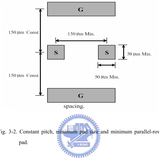
(41) Chapter 3 Experimental Procedure of High-κ MIM Capacitor with Al doped TaOx Dielectrics. 3.0 Microwave Layout Rules for On-wafer Measurement Mechanical 1. GSG Configuration Metal pads must be laid out with ground-signal-ground (GSG) probe configuration as shown in Fig. 3-1. 2. Pad Pitch: All pads contacted by an individual probe must be collinear with a constant center-to-center pad pitch of 150 µm as shown in Fig. 3-2. 3. Pad Size The minimum pad size is 50µm × 50 µm as shown in Fig. 3-2. 4. Passivation Window The minimum passivation window size is 96µm × 96 µm. The passivation window must be larger than the probe contact. If the pad metalization is above the final passivation layer, this rule does not apply. 5. Parallel-Row Pad Spacing. 25.
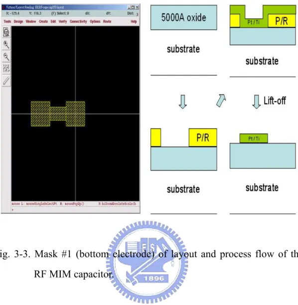
(42) The minimum center-to-center pad spacing between facing probes is 150 µm as shown in Fig. 3-2. Note that this spacing is based on the assumption of 750 µm of probe vertical overtravel. 6. Pad Height Variation The minimum pad height variation in a row of pads contacted by one probe is 0.5 µm. 7. Planarity Requirements The maximum overall planar deviation of a row of pads contacted by one probe, with respect to the backside of the substrate is 2/1000. Electrical Maximum Rated Current The maximum dc current in port 1 is 0.1 ampere while that in port 2 is 0.5 ampere and the maximum dc current per contact is 0.5 ampere.. 3.1 The Fabrication Process Flow of Al doped TaOx MIM Capacitors The MIM capacitors were fabricated using 4-in p-type or n-type Si wafers. To integrate the high-κ capacitors into VLSI backend process, we started with 500 nm isolation oxide deposition on Si wafers by Wet Oxide furnace. The bottom electrode of MIM capacitor was formed by Electron-gun (E-gun) on the isolation oxide using Pt/Ti (Pt/Ti = 90nm/10nm) bi-layer metals as shown in Fig. 3-3. The bottom electrode. 26.
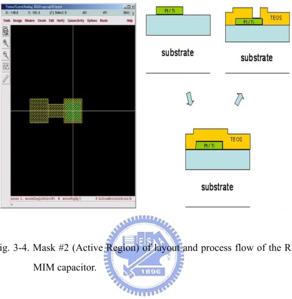
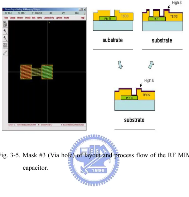
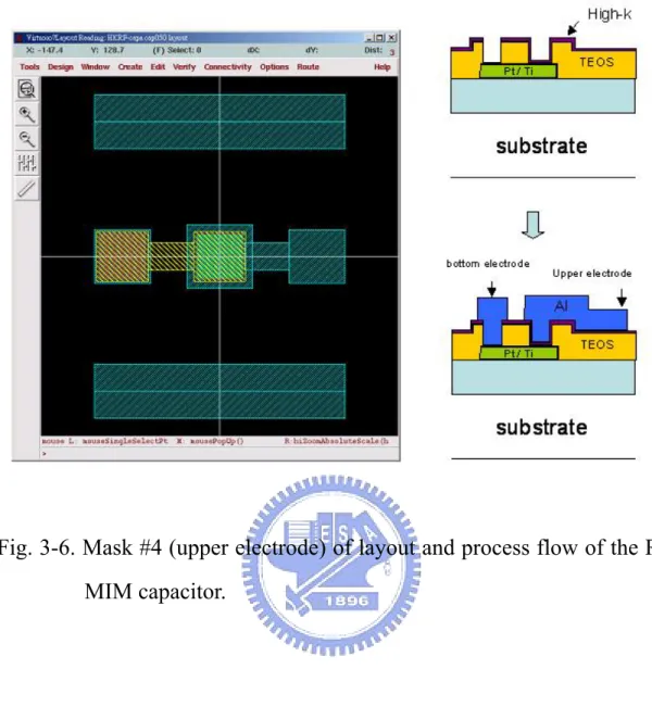
(43) was also patterned using Lift-off technology to form the coplanar transmission line for RF measurement. A plasma-enhanced chemical vapor deposition (PECVD) passivation oxide was deposited for isolation and followed by patterning the active capacitor region as shown in Fig. 3-4. Then high-κ Al doped TaOx was formed by depositing Al and Ta (Al:Ta = 1:8) metals on Pt electrode followed by oxidation at 400 oC [3.1] for 45 min and subsequent annealing for 15 min. The above process fits well the low thermal budget requirement of current VLSI backend integration. Various different thicknesses from 11.5 to 25.5 nm are formed and confirmed by ellipsometer measurement. The reason for doping AlOy into TaOz is to preserve the merit of good MIM capacitor integrity by adding Al2O3 dielectric. Addition of Al2O3 [3.2] to Ta2O5 reduces the leakage current, although this results in a slightly lower κ-value [3.3]-[3.4]. Then via hole was patterned shown in Fig. 3-5. Finally, Al metal was deposited on high-κ dielectrics followed by patterning to form the top electrode of MIM capacitor and coplanar transmission line for RF measurements shown in Fig. 3-6. The typical MIM capacitor area is 50 µm × 50 µm. Fig. 3-7 and Fig. 3-8 show the MIM capacitor cross-section view and layout view, respectively. The detailed fabrication process flow is listed as follows: 1. (100) orientation n-type or p-type Si wafer. 2. Initial cleaning (RCA clean). 27.
(44) 3. Thermal wet oxidation at 1036 oC to grow 500 nm thermal SiO2 in furnace. 4. Depositing Pt/Ti (Pt/Ti = 90nm/10nm) bi-layer metals, Ti first, by E-gun, then employing Lift-off technology. 5. A PECVD passivation oxide 100nm was deposited for isolation and followed by patterning the active capacitor region. 6. Then high-κ Al doped TaOx was formed by depositing Al and Ta (Al:Ta = 1:8) metals on Pt electrode. 7. Following by oxidation at 400 oC for 45 min and subsequent annealing for 15 min in furnace. 8. Then via hole was patterned. 9. Finally, Al metal was deposited on high-κ dielectrics by thermal coater followed by patterning to form the top electrode of MIM capacitor and coplanar transmission line.. 3.2 The Measurement of Al doped TaOx MIM Capacitors The high-κ MIM capacitors were characterized using an HP4284A precision LCR meter from 10 KHz to 1 MHz. Above 1 MHz the S-parameters (Fig. 3-9) were measured using an HP8510C network analyzer (from 200 MHz to 20 GHz). Additional “OPEN” dummy device [3.5] shown in Fig. 3-10 were measured to. 28.
(45) de-embed the parasitic capacitance in the RF layout of the MIM capacitor. A similar method was used for RF noise analysis in 0.18 to 0.13 µm MOSFETs [3.6]. So the measured S-parameters were de-embedded from a dummy device and the RF frequency capacitance plus parasitic parameters were extracted using an equivalent circuit model shown in Fig. 3-11. The parasitic pad, series inductor and resistor in transmission line are de-embedded from a same line length through transmission line [3.7]-[3.8].. 3.3 De-embedding Theory When circuits or devices work at high frequencies, many parasitic effects will happen. For example, a signal applied on one metal line, the potential of this metal line at any point is equal if the wavelength of signal is long enough, compared with metal line. But the potential of the metal line at any potential will be different when the wavelength of signal can compare with the metal line or shorter, i.e. high frequency signal. Hence, a metal line was regarded as a resistor at low frequency or resistor plus parasitic inductance and capacitance parameters at high frequency in an equivalent circuit model. In order to measure this MIM capacitance, we must layout additional probe pads and signal lines for measurement. However, these added potions will generate additional parasitic effects. So we must de-embed these parasitic 29.
(46) parameters to get the intrinsic high frequency capacitance. Fig. 3-12 shows the equivalent circuit of a RF MIM capacitor device at high frequency. As devices were measured approach microwave frequency, we can not directly measure the lump circuit components, like RLC (resistance, inductance and capacitance), because of parasitic effects. Scattering-parameters (S-parameters) were obtained in general [3.9]. According to microwave theorem [3.9], we can transform the S-parameters into an equivalent circuit model to extract the component that we want. Among added portions for measurement, the parasitic capacitance effects dominate in probe pads. We can transform both of the measured S-parameters of MIM capacitors and “OPEN” dummy device into admittance parameters (Y-parameters). Then we de-embed the parasitic capacitance effects form the MIM capacitor by YMIM-YOPEN. So we can get the de-embedded S-parameters from the transformation of de-embedded Y-parameters. We have de-embedded the parasitic shunt capacitance effects due to the probe pads of MIM capacitor. Then, we use an equivalent circuit method to simulate the de-embedded S-parameter shown in Fig. 3-9 to extract each components of the equivalent circuit model shown in Fig. 3-11 by Series Ⅳ. From this, we can obtain the RF capacitance of MIM capacitor.. 30.
(47) Fig.. 3-1.. Typical. layout. suitable. for. coplanar. probing. ground-signal-ground (GSG) probe configuration. 31. with.
(48) Fig. 3-2. Constant pitch, minimum pad size and minimum parallel-row pad.. 32.
(49) Fig. 3-3. Mask #1 (bottom electrode) of layout and process flow of the RF MIM capacitor.. 33.
(50) Fig. 3-4. Mask #2 (Active Region) of layout and process flow of the RF MIM capacitor.. 34.
(51) Fig. 3-5. Mask #3 (Via hole) of layout and process flow of the RF MIM capacitor.. 35.
(52) Fig. 3-6. Mask #4 (upper electrode) of layout and process flow of the RF MIM capacitor.. 36.
(53) Fig. 3-7. The RF MIM capacitor cross section view.. 37.
(54) Fig. 3-8. The RF MIM capacitor layout view.. 38.
(55) 1.0 EOT = 2.0nm 2.4nm Measured simulated. 2.0. 0.5 0 1.0. S21. -0.5 S11 -1.0 -2.0. Fig. 3-9. Measured and simulated scattering parameters of 2.0 and 2.4 nm EOT Al doped TaOx MIM capacitors.. 39.
(56) Fig. 3-10. The “OPEN” dummy structure for the device under test (DUT) modeled in the shunt configuration.. 40.
(57) LS1 = 0.01nH. RS = 10Ω. RP. = 1.5/2.0kΩ. LS2 = 0.01nH. C = 41.0/36.5pF. Fig. 3-11. The equivalent circuit model and numerical values of elements for capacitor simulation at RF regime.. 41.
(58) Fig. 3-12. The equivalent circuit model of MIM capacitor at RF regime.. 42.
(59) Chapter 4 The Characteristics of High-κ MIM Capacitor with Al doped TaOx Dielectrics. 4.1 Capacitor Characteristics For precision analog circuit applications, the MIM capacitors need to be useful over wide range of frequencies. To further study the RF frequency characteristics, we have measured the S-parameters up to 20 GHz. Fig. 4-1 shows the measured (de-embedded) and modeled S-parameters for Al doped TaOx MIM capacitors, where the modeled data is from the equivalent circuit model shown in Fig. 4-2. The RS, LS, RP, and C in the model are the parasitic series resistor, series inductor, parallel resistor, and capacitor, respectively. Good agreement between measured and modeled data is obtained that suggesting the good accuracy of physically based equivalent circuit model for both capacitors with different thickness, which can be used for capacitance extraction. The capacitance values were measured directly using the LCR meter from 10 KHz to 1 MHz and calculated from the measured (de-embedded) S-parameters up to 20 GHz using the equation [4.1]: ∆ C Z 0 ( 2 + Z (C ) / Z 0 ) 2 = jωC 2 ( RP + 1 / jω C ) 2 ∆ ( S 21 ) 2 C 2 RP. 43. (1).
(60) Z (C ) = RS + jω ( LS 1 + LS 2 ) + S 21 =. RP / jω C RP + 1 / jω C. 2 2 + Z (C ) / Z 0. ( 2) (3). We can use the equation (1) to derive the capacitance densities at different frequencies. Z(C) in equation (2) is the total impedance in the equivalent circuit model of Fig. 4-2 and Z0 is the characteristic impedance of transmission line. The RF frequency ∆C/C in equation (1) is obtained by differentiating the measured S21 in equation (3), where shows the relation between the S21 and total impedance Z(C). Fig. 4-3 shows that the derived ∆C/C decreases rapidly with increasing frequency, which is advantageous for high frequency analog/RF circuits. Figs. 4-4 and 4-5 show the C-V characteristics and ∆C/C for Al doped TaOx MIM capacitors with physical thickness of 11.5 and 14.0 nm, respectively. Capacitance densities at RF regime have been extracted in pervious work using equivalent modeling circuit fitting from measured S-parameters [4.2]-[ 4.4] and are also plotted in the figure. At 100 kHz frequency, high capacitor density of 17 and 15 fF/µm2 are measured for 11.5 and 14 nm respectively, and a κ value of 22 is obtained for. Al. doped. TaOx. dielectrics.. The. equivalent-oxide. thickness. (EOT,. teq=κox*thigh-κ/κhigh-κ) values for these high-density capacitors are calculated to be 2.0 and 2.4 nm for 11.5 and 14.0 nm physical dielectric, respectively. Fig. 4-6 shows the J-V characteristics of Al doped TaOx MIM capacitors. The asymmetrical J-V and. 44.
(61) breakdown voltages under positive and negative bias are due to the different work function of top Al and bottom Pt electrodes. The leakage current is increased by trading off the increasing capacitance density, and values of 4.5×10⁻⁷ and 8.9×10⁻⁷ A/cm2 are measured at -2 V for respective EOT of 2.4 and 2.0 nm. The leakage current, 8.9×10⁻⁷ A/cm2, is low enough for circuit applications. This arises because the high capacitor density requires using only a small area. This is shown by the small leakage current of 5.2×10⁻¹² A of a large 10 pF capacitor, which is even smaller than the leakage current of a 0.13-µm MOSFET [4.5]. Note that ∆C/C in Fig. 4-3 decreases with increasing frequency. This is an advantage at the high operational frequencies of analog/RF circuits. Fig. 4-7 shows the frequency dependence of both the capacitance and Q-factor for high-κ Al doped TaOx MIM capacitors. Below 1 MHz, the Q-factor was derived from the measured loss tangent using 1/tanδ. At higher frequencies an equivalent circuit model was used to determine the C value and the Q-factor from the measured S-parameters. Only a small capacitance reduction (5%) occurs from 10 KHz to 10 GHz, which is attractive for RF applications. The Q-factor increase up to ~ 8 GHz is due to the resonance of the MIM capacitor with a parasitic inductor. The relatively low resonant frequency of ~8 GHz arises from the very large capacitance (42.5 pF) and the residual. 45.
(62) inductance, even after de-embedding. A Q-factor of ~ 40 before resonance for the 17 fF/µm2 capacitors is a desirable characteristic. The high capacitance density, low leakage current, small frequency dependence and good Q-factor for these Al doped TaOx MIM capacitors are useful and important for analog and RF circuit applications.. 4.2 The Normalized Capacitance Variation ∆C/C and Voltage Coefficient of Capacitance VCC To further study the frequency dependence of ∆C/C and related quadratic VCC (α), we have plotted ∆C/C and α as a function of frequency in Fig. 4-8. The relation between α and ∆C/C is expressed in the following equation: C (V ) − C (0) ∆C = αV 2 + β V × 10 6 = C C (0) ppm . (4). The β is the linear VCC, which is less important than α by using circuit cancellation method [4.6]. Again, the ∆C/C and α decrease monotonically with increasing frequency. Small ∆C/C ≤ 120 ppm and α ≤ 280 ppm/V2 are obtained with increasing frequency into GHz regime indicating that the high-κ MIM capacitors can be used for precision circuits with GHz operation frequency. Such high frequency is required since the operation speed of MOSFET continuously increases with device scaling down and the commercially available CPU circuit is already several GHz.. 46.
(63) We have also plotted the ∆C/C and α as a function of 1/C (or equivalent to td since 1/C=td/ε0κ) in Fig. 4-9. Both ∆C/C and α decrease with increasing frequency similar to the trend shown in Fig. 4-8. In addition, the ∆C/C and α decrease with increasing ln(1/C) or ln(td) regardless the using different high-κ dielectrics [4.7]. Although the detailed physics to explain such dependence is still under investigation, possible reason may be related to the leakage current through dielectric and/or carrier trapping or de-trapping inside the high-κ dielectric.. 4.3 The Temperature Coefficient of Capacitor TCC In additional to the requirement of small ∆C/C and α dependence on voltage, the small TCC is another important factor for precision analog circuit application. Figs. 4-10 and 4-11 show the respective ∆C/C versus temperature and TCC of the Al doped TaOx capacitors at different frequencies with two different dielectric thicknesses of 3.3 and 4.8nm EOT. The temperature dependent ∆C/C decreases with increasing frequency that is consistent with the decreasing trend in Fig. 4-8. The ∆C/C in both high-κ capacitors increases with increasing temperature that shows the same trend with other dielectric capacitors published in the literature [4.8]. We have further plotted the TCC as a function of 1/C (or equivalent to td) in Fig. 4-12 from the measured temperature dependence on ∆C/C. The TCC is also higher at thinner thickness and decreases monotonically with increasing frequency from 10 kHz. 47.
(64) to 1 MHz. It is noticed that the TCC in both high-κ dielectrics decreases rapidly with increasing ln(1/C), and the extrapolated data is close to previous TCC data of HfO2 [4.7] at the same 1/C. Such exponential dependence of TCC on 1/C or td is similar to the dependence of ∆C/C and α on ln(1/C) in Fig. 4-9. Although the physical meanings are currently under study, possible reason may still be related to the leakage current through dielectric and/or carrier trapping or de-trapping inside the high-κ dielectric due to their temperature dependence in physics.. 48.
(65) 1.0 EOT = 2.0nm 2.4nm Measured simulated. 2.0. 0.5 0 1.0 S21. -0.5 S11 -1.0 -2.0. Fig. 4-1. Measured and simulated scattering parameters of 2.0 and 2.4 nm EOT Al doped TaOx MIM capacitors at RF regime.. 49.
(66) LS1 = 0.01nH. RS = 10Ω. RP. = 1.5/2.0kΩ. LS2 = 0.01nH. C = 41.0/36.5pF. Fig. 4-2. The equivalent circuit model and numerical values of elements for capacitor simulation at RF regime.. 50.
(67) 5. 10. EOT 2.0nm EOT 2.4nm. 4. ∆C/C (ppm). 10. 3. 10. 2. 10. 1. 10 3 10. 4. 10. 5. 10. 6. 10. 7. 10. 8. 10. 9. 10. 10. 10. 11. 10. Frequency (Hz). Fig. 4-3. The ∆C/C of Al doped TaOx MIM capacitors as a function of frequency. It is notice that the ∆C/C decrease with increasing frequency.. 51.
(68) 6. 20. 10. 15 10 KHz 100 KHz 1 MHz 1 GHz 10 GHz. 10. 5. 0 -1.6. 4. 10. 3. 10. ∆C/C (ppm). 2. Capacitance (fF/µm ). 5. 10. 2. 10. 1. -1.2. -0.8. -0.4. 0.0. 0.4. 0.8. 1.2. 10 1.6. Voltage (V). Fig. 4-4 C-V and ∆C/C-V characteristics of MIM capacitors with 2.0 EOT Al doped TaOx dielectrics at different frequencies from 10 KHz to 10 GHz. The voltage is applied to the bottom Pt electrode. Measured area is 50mm × 50mm.. 52.
(69) 6. 10 10 KHz 100 KHz 1 MHz 1 GHz 10 GHz. 12. 5. 10. 4. 10. 8 3. 10 4. 0 -1.6. ∆C/C (ppm). 2. Capacitance (fF/µm ). 16. 2. 10. 1. -1.2. -0.8. -0.4. 0.0. 0.4. 0.8. 1.2. 10 1.6. Voltage (V). Fig. 4-5. C-V and ∆C/C-V characteristics of MIM capacitors 2.4 nm EOT Al doped TaOx dielectrics at different frequencies from 10 KHz to 10 GHz. The voltage is applied to the bottom Pt electrode. Measured area is 50mm × 50mm.. 53.
(70) -3. 2. Leakage Current Density (A/cm ). 10. -4. 10. -5. 10. -6. 10. -7. 10. 2.0nm EOT 2.4nm EOT. -8. 10. area = 50µm x 50µm. -9. 10. -8. -6. -4. -2. 0. 2. 4. 6. Voltage applied on bottom electrode (V). 8. Fig. 4-6. J-V characteristics of 2.0 and 2.4 nm EOT Al doped TaOx MIM capacitors. The asymmetric J-V and breakdown voltages are due to the different bottom Pt and top Al electrodes.. 54.
(71) 20. 700. 15. 10. 500. 2.0nm EOT 2.4nm EOT. 400 300. Quality Factor. 2. Capacitance (fF/µm ). 600. 200. 5. 100. 0 1k. 10k. 100k. 1M 10M 100M Frequency (Hz). 1G. 10G. 0. Fig. 4-7. The frequency dependent capacitance and Q-factor of 2.0 and 2.4 nm EOT Al doped TaOx MIM capacitors.. 55.
(72) 2. Quadratic VCC α (ppm/V ). 7. 8. 10. α. AlTaOx 2.0 nm EOT. 6. 10. 7. 10. AlTaOx 2.4 nm EOT HfO2 [4.7]. 5. 10 ∆C/C (ppm). 10. ∆C/C. 6. 10. 4. 10. 5. 3. 10. 2. 10. 1. 10. 0. 10 100G. 10. 4. 10. 3. 10. 2. 10. 10. 1k. 1. 10k. 100k. 1M. 10M. 100M. 1G. 10G. Frequency (Hz). Fig. 4-8. The ∆C/C and a of Al doped TaOx MIM capacitors as a function of frequency. It is notice that the ∆C/C and a decrease with increasing frequency.. 56.
(73) 2. Quadratic VCC α (ppm/V ). 5. 6. 10. α. ∆C/C. 10 kHz 100 kHz 1 MHz 1 GHz 10 GHz. 4. 10. ∆C/C (ppm). 3. 10. 5. 10. 4. 10. 2. 10. 3. 1. 10. 10. 2. 10. 0. 10. AlTaOx. HfO2 [4.7]. -1. 10. 10. 0.0. 1. 10. 0. 2 0.1 0.2 0.3 1/Capaictance Density (µm /fF). 10 0.4. Fig. 4-9. The ∆C/C and α of Al doped TaOx MIM capacitors as a function of 1/C. It is notice that the ∆C/C and αdecrease monotonically with ln(1/C).. 57.
(74) 80000 AlTaOx. 70000. 3.3 nm 4.8 nm EOT 10 kHz 100 kHz 1 MHz. ∆C/C(ppm). 60000 50000 40000 30000 20000 10000 0 0. 25. 50. 75 100 o Temperature ( C). 125. 150. Fig. 4-10. The ∆C/C as a function of temperature of Al doped TaOx MIM capacitors.. 58.
(75) 4. 10. AlTaOx 3.3 nm EOT AlTaOx 4.8 nm EOT. o. TCC (ppm/ C). 3. 10. 2. 10. 1. 10. 1k. 10k. 100k. 1M. 10M. Frequency (Hz). Fig. 4-11. The TCC as a function of frequency of Al doped TaOx MIM capacitors.. 59.
(76) o. TCC (ppm/ C). 1000. 100 AlTaOx. 10 0.0. 0.1. HfO2[4.7] 10 kHz 100 kHz 1 MHz. 0.2. 0.3. 0.4. 0.5. 2. 1/Capaictance Density (µm /fF). Fig. 4-12. The TCC of Al doped TaOx MIM capacitors as a function of 1/C. TCC decreases monotonically with ln(1/C).. 60.
(77) Chapter 5 The Theorem of the Variation of Dielectric Constant. 5.1 Introduction of Free-carrier Relaxation After recalling the background of Debye’s relation for dipole relaxation, we give a detail presentation for the derivation of the complex dielectric constant due to the contribution of space charges that made of free carriers able to move between blocking electrodes. Then we propose experimental tests of the model to discuss the formal analog between the relaxation of a collection of permanent dipoles and that of space charges.. 5.2 Debye Formula Dipole relaxation within the meaning of Debye is a purely viscous process without elastic forces of recovery. A typical equation for such a phenomenon is, for example, that which describes the speed ν of a particle of mass m after the application of a constant force F in a viscous medium. Exerting a friction force fν on the particle to move:. m. dv = F − fv dt. (1). If the particle, having charge Q, is in a field E, then the force F is qE. The relation. 61.
(78) (1) can be written in the form: dv v s − v = dt τ. ( 2). where τ = m/f and νs is the speed limit (static) νs = F/f taken by the particle. By analogy, we can write for polarization by Por, orientation of whole dipoles in thermal balance: dPor 1 = [ Ps − Pi − Por (t )] dt τ. (3). here, τ indicates the dipolar relaxation time, Ps is the end value (static) of polarization in a continuous-current field and Pi is the initial value which corresponds to quasi-instantaneous polarization due to the dependent electrons and ions (Por → Ps - Pi in a constant field). Let us imagine now that the particles (or, by analogy, dipoles) are in an alternate field of the form: E = E 0 e iωt. (4). In alternative mode, all the variables, and in particular polarization by Por orientation, oscillate sinusoidal with the pulsation ω, so that we can write: Por (t ) = Por e iωt. (5). We can directly obtain (if not rigorously) the formula of Debye while replacing in (3) dPor/dt by his value iωPor drawn from (5): iωτ Por = Ps − Pi − Por. (6). 62.
(79) We derive that: Por (ω ) =. Ps − Pi 1 + iωτ. (7). so that the total polarization P(ω), sum of instantaneous polarization Pi and the polarization of Por, is written: P (ω ) = Pi +. Ps − Pi 1 + iωτ. (8). By admitting that the local field of the dipoles is equal to the field applied. One has, by definition of the permittivities: P * (ω ) = (ε * − ε 0 ) E. (9). Pi (ω ) = (ε ∞ − ε 0 ) E. (10). and Ps (ω ) = (ε s − ε 0 ) E. (11). so that the relation (8) becomes:. ε * (ω ) = ε ∞ +. εs −ε∞ 1 + iωτ. (12). the relation (12) is the famous formula of Debye.. 5.3 Polarization by Space Charges In. the. traditional. treatments. of. the. interfacial. polarization. of. the. Maxwell-Wagner type, one admits that the movement of the instantaneous charges in material does not affect the uniform distribution of the field. In fact, the changes. 63.
(80) accumulate in the electrodes, in which they discharge more or less easily. It results from the gradients of concentration which tend to be opposed to accumulation. Briefly, the model treated initially by Mac Donald [5.1], who makes the following assumptions: 1. The material contains completely ionized fixed centers (for example, energy levels of impurities very close to the conduction band) and, mobility µ of free electrons in equal concentration. 2. The electrodes are completely blocking so that the current of electrons at the balance of the electrodes (x = ± d) are null. In the absence of field applied, the free electrons, uniformly distributed in the sample, compensate for the load of the positive ionized centers everywhere, so that the sample is neutral. In the presence of a continuous-current field applied, the electrons are distributed in the sample under the combined action of the field and the diffusion which tends to be opposed to their accumulation to the electrodes. If ρ(x) is the density of charge to balance with depth x in the sample index, average polarization is written: P=∑p P=. 1 2d. ∫. (13) d. −d. xρ ( x) dx. (14). If the direction of the field applied is then reversed, the electrons are distributed again. 64.
(81) and the situation develops towards a new balance where ρ’(x) = - ρ(x). Therefore, the new macroscopic dipole and polarization are opposed to the precedent. We thus attend a phenomenon similar to a dipolar relieving of Debye type, occurring in a sample that becomes from initially homogeneous (statistically) to heterogeneous under the action of the field. This is represented on figure 5-1.. 5.4 Calculation of Polarization into Alternative Field Following, we will study the dynamic balance of the system when the sample is subjected to an alternate field of pulsation ω and rather low amplitude so that the system remains linear, and consequently that the variables (time and space) are separable. In fact, it is more about a limit on the tension applied (at ordinary temperature). We concern for the uniform concentration n0 and their mobility µ of free electrons (and centers) in the absence of alternating field. Under the terms of the assumptions, the total number of electrons per unit area of the sample, thickness 2d, is equal to 2dn0 in the presence of the alternate field. That is to say: E a = Aa e iωt. (15). the alternate field applied, whose amplitude Aa assumes lower than KT/2. The. 65.
(82) concentration of charge at x-coordinate x is not very different from n0, so that the difference n - n0 oscillates with the pulsation ω and we can write: n( x, t ) = n0 + v( x) e iωt. (16). In the same way, the potential V(x,t) and the field E(x,t) take the respective forms: V ( x, t ) = ϕ ( x) e iωt. (17). and E ( x, t ) = A( x) e iωt. (18). Of course, the factors ν(x), ϕ(x) and A(x) are complex quantities. The complex permittivity ε*(ω) of the sample is by definition:. ε* =ε +. P(ω ) Aa. (19). where polarization P, defined by (14), results from the excess of density ν(x), given by (16). Calculation of ν(x) is the current of particles and the number of charges crossing to x-coordinate x, by unit time, unit area of the x-plane. It is the sum of the drift current nµE and the diffusion current -- D ∇ n: j ( x, t ) = − µn. ∂V ∂n −D ∂x ∂x. (20). so that the conservation equation: ∂n ∂j =− ∂t ∂x 66.
(83) becomes ∂n ∂ ∂V ∂2n = µ (n )+D 2 ∂t ∂x ∂x ∂x. (21). While introducing the values of n and V into (21), given from (16) and (17) respectively, we can obtain: iωv = µn0. d 2ϕ d 2v d dϕ + D + µ (v )e iωt 2 2 dx dx dx dx. (22). Since ν is small compared with n0, the third term of the member of right-hand side of (22) is negligible compared with the first two terms. In addition, the Poisson's equation is written here: d 2ϕ e =− v 2 ε dx. (23). and, while combining (23) with the simplified equation (22), we can obtain: (iω +. µen0 d 2v )v = D 2 ε dx. (24). Then we regard µen0/ε = σ/ε as the reverse of the relaxation time τ of material, (24) is written in the form: d 2 v 1 + iωτ = v Dτ dx 2. (25). By using the variable complexes reduced: X =. Z 1 + iωτ x= x Dτ L. where Z = (1+iωτ)1/2 and L = (Dτ)1/2 is the length of Debye, d 2v =v dX 2. (26). This equation has as a general solution:. 67.
(84) v = v1 e X + v 2 e − X but the conservation of the instantaneous charges implies:. ∫. d. −d. v( x) dx = 0. It indicates ν2 = - ν1, so that the solution physically acceptable for ν(x) is: v( x) = 2 v1 sinh(. Z x) = 2 v1 sinh X L. (27). By integrating (23), we can obtain: 2ev1 L cosh X + A0 ε Z. A( x) =. (28). and the constant A0 results from the boundary condition imposed by the potential applied:. ∫. d. −d. A( x) dx = 2 Aa d. which is written: 2ev1 L 2 ( ) sinh Y + A0 d = Aa d ε Z. (29). where we posed: Y = X (d ) = (d ) Z = L =. δ. 2. [( 1 + ω 2τ 2 + 1). 1. 2. 1. + i ( 1 + ω 2τ 2 − 1) 2 ]. was left that (28) takes the form: A( X ) = Aa +. 2edv1 sinh Y (cosh X − ) Y ε Y. (30). Finally, ν1 can be obtained by writing that the current of particles in x = d (X = Y) is null, since the electrodes are blocking:. 68.
(85) nµA(Y ) − D. Z dv ( )Y = 0 L dX. (31). Taking (27) and (30) into account, (31) is written: Aa +. 2edv1 2 DZv1 sinh Y (cosh Y − )= cosh Y Y nµL ε Y. (32). By remembering that n ~ n0 and using the written accounts above between L, D, µ and n, (32) takes the form: Aa =. 2ev1. ε. [( LZ −. L L sinh Y ) cosh Y + ] Z Z Y. (33). and like LZ – L/Z = iωτL/Z, the relation above gives ν1, and consequently: v( x) = 2v1 sinh X =. εZAa. sinh X eL iωτ cosh Y + sinh Y. (34) Y. Consequently, the polarization given by (14) becomes: P(ω ) =. εAa. ∫. Y. 0. X cosh X dX. Y iωτ cosh Y + sinh Y. (35) Y. After integration of the numerator: P(ω ) = εAa. cosh Y − sinh Y. Y sinh Y iωτ cosh Y +. (36) Y. While returning to the definition of P(ω) (19), we have finally obtained:. ε* =ε. 1 + iωτ iωτ + tanh Y. (37) Y. The relation (37) was extended by Meaudre and Mesnard [5.2]-[5.3] if we take account of the existence of traps in material. Y must be modified.. 69.
數據
![Fig. 2-1. Schematic of important regions of a field effect transistor gate stack [2.20]](https://thumb-ap.123doks.com/thumbv2/9libinfo/8760610.208089/32.892.258.637.111.524/fig-schematic-important-regions-field-effect-transistor-stack.webp)
![Fig. 2-5. TEM cross section of 7 nm Ta 2 O 5 on silicon. The 2.0 nm film is a SiTa x O y interfacial region [2.22]](https://thumb-ap.123doks.com/thumbv2/9libinfo/8760610.208089/36.892.149.744.121.517/fig-tem-cross-section-silicon-sita-interfacial-region.webp)
![Fig. 2-6. Reduction of gate capacitance due to formation of SiO 2 interfacial layer after 800 o C crystallization [2.22]](https://thumb-ap.123doks.com/thumbv2/9libinfo/8760610.208089/37.892.241.650.110.531/fig-reduction-gate-capacitance-formation-interfacial-layer-crystallization.webp)
![Fig. 2-8. Current-voltage relations for Ta-Al-O showing the improvement of electrical properties of Ta 2 O 5 with addition of Al [2.22]](https://thumb-ap.123doks.com/thumbv2/9libinfo/8760610.208089/39.892.143.749.109.730/current-voltage-relations-showing-improvement-electrical-properties-addition.webp)
+7
![Fig. 2-9. Dielectric constant of Ta-Al-O as a function of Al concentration in the sputtered films [2.22]](https://thumb-ap.123doks.com/thumbv2/9libinfo/8760610.208089/40.892.154.745.113.525/fig-dielectric-constant-ta-function-concentration-sputtered-films.webp)
Outline
A Modified Model for the Variation of the Capacitance above 1 MHz
The Characteristics of High-κ Dielectrics
The Choice of High-κ Dielectrics
De-embedding Theory
The Temperature Coefficient of Capacitor TCC
Calculation of Polarization into Alternative Field
Stress Induced Voltage Coefficient of Capacitance
Analysis of the Variation of Capacitance
相關文件
z 圖3-39所示為電感性電 路電流增加率與時間的 關係。在第一個時間常 數的時段裡電流上升到 最大值的63.2%,而在第
C.轄屬各樂齡學習中心 數超過 25 所者,103 年 度於平面媒體(含報 紙、雜誌)刊出達 12 則 以上,並結合廣播電
• 接續之前的例子,若原為 0.288 pF 的液晶 電容 C LC ,再並聯一個亦為 0.288 pF 的電 容C st ,則電位保持的變化值為.
鋼絲軌道: (鋼絲型線燈)利用 金屬線的導電性取代傳統 電線。線燈多採用多面反 射燈泡。.. 特殊燈.
◦ 金屬介電層 (inter-metal dielectric, IMD) 是介於兩 個金屬層中間,就像兩個導電的金屬或是兩條鄰 近的金屬線之間的絕緣薄膜,並以階梯覆蓋 (step
5.電視表現的形式與風格 從電視螢光幕談起,介紹電視如何傳送畫 面,以及電視的節目內容有哪些風格 6.電視科技發展
Ex.3 the threshold value U t ( 150 mJ) required to ignite airborne grains... 5-3 Capacitors
(2) 被動式 RFID Tag(Passive):被動式 RFID Tag 不含電池,其能量是 感應自 RFID Reader 所發射過來的 RF 無線電波能量,當 RFID
