行政院國家科學委員會專題研究計畫 成果報告
費米能階釘札效應,準分子雷射加工與乾蝕刻技術應用於 P
型氮化鎵蕭特基二極體製作之研究
計畫類別: 個別型計畫
計畫編號: NSC93-2215-E-018-005-
執行期間: 93 年 08 月 01 日至 94 年 07 月 31 日
執行單位: 國立彰化師範大學光電工程技術研究所
計畫主持人: 林祐仲
計畫參與人員: 朱宥霖,林文祥,吳國禎
報告類型: 精簡報告
處理方式: 本計畫可公開查詢
中 華 民 國 94 年 7 月 4 日
1
研究計畫中文摘要:
關鍵字﹕ 氮化鎵,蕭特基二極體,表面費米能階釘札,乾蝕刻
目前,氮化鎵族群的藍色發光二極體及雷射的性能提昇上,除必須有良好
的磊晶結構之外,必須有性能良好的 p 型及 n 型歐姆接觸特性。由於目前 p 型氮
化鎵磊晶層之電洞濃度無法有效的提高,因此要達到金屬/p 型氮化鎵的歐姆接觸
較為困難。在 p 型氮化鎵的歐姆接觸研究已有諸多成果被發表,反觀 p 型氮化鎵
的蕭特基接觸的研究並不多,其已發表之文獻報導所觀測的位障高度差異甚大,
並未有明確的機制被建立。此次研究將主持人先前對 p 型氮化鎵的歐姆接觸的研
究成果應用於 p 型氮化鎵蕭特基二極體中歐姆電極製作,因為良好歐姆電極將有
助提昇 p 型氮化鎵蕭特基二極體之電特性,此外,再利用乾蝕刻處理(反應離子
蝕刻或感應耦合電漿蝕刻技術)或準分子雷射加工處理產生 p 型氮化鎵表面施體
型缺陷引發費米能階釘札效應提高 p 型氮化鎵蕭特基二極體之蕭特基電極與 p
型氮化鎵間之障壁,降低漏電流。本次計畫成果將有助於對 p 型氮化鎵之材料特
性有所了解、製作優良之 p 型氮化鎵蕭特基二極體,而且也能改善金屬/p 型氮化
鎵的歐姆接觸進而提高藍光二極體的效能。另一方面,對於發展氮化鎵的光檢測
也有極大的助益。
研究計畫英文摘要:
Keywords: GaN, Schottky diodes, Barrier height, Surface Fermi level pinning,
Dry etching
GaN continues to grow in importance for the high-brightness light emitting
diodes (LEDs) in the visible and ultraviolet wavelength regions. For the case of the
highly efficient LED, several critical problems must be addressed, such as high hole
concentration in p-type GaN (p-GaN) and low-resistance ohmic contact in the
fabrication processes for the devices. High-quality ohmic and Schottky contacts are
required for the improvement of these devices. The ohmic-contact characteristics of
metal contact on p-GaN have been relatively established. Only a few studies of barrier
height on p-GaN have been reported in the literature, likely due to the difficulties in
measuring diodes with large leakage and large series resistance. The contacts tend to
exhibit very leaky Schottky characteristics. Consequently, the mechanism of current
flow through the interface has not been established and the exact value of Schottky
barrier height has not yet been estimated. The p-GaN ohmic-contact technique
reported in our previous published paper shall be applied in this study. Good ohmic
contacts will help to obtain the actual p-GaN Schottky characteristics. In addition, the
applications of the dry etching and an excimer laser treatment in the fabrication of
p-GaN Schottky contacts will induce the formation of the surface defects on the
p-GaN surface, the pinning of the Fermi level on the p-GaN surface and the
enhancement of the Schottky barrier height at the metal/p-GaN interface. So in this
plan, we are devoted to improve the p-GaN Schottky contact.
2
計畫成果自評:
本次計畫研究內容與原計畫相符程度達 80%,並達成預期目標,而且研究
成果五篇論文均已發表於國際知名期刊,獲得國際學者肯定,極具學術與實際應
用之價值。
結案報告內容:
此次專題計畫研究成果已撰寫成五篇論文並發表於美國國際期刊,依序列於
下:
1. Y. J. Lin, 2005, March
“Appl
i
c
a
t
i
on
of
t
he
t
he
r
mi
oni
c
f
i
e
l
d
e
mi
s
s
i
on
mode
l
i
n
t
he
study of a Schottky barrier of Ni on p-GaN from current-v
ol
t
age
mea
s
ur
eme
nt
s
”
,
Appl. Phys. Lett. Vol.86, 122109.
2. Y. J. Lin and Y. L. Chu, 2005, May
“
Effect of reactive ion etching-induced
defects on the surface band bending of heavily Mg-doped p-type GaN”
,
J. Appl.
Phys. Vol.97, 104904.
3. Y. J. Lin, Y. L. Chu, Y. S. Huang, and H. C. Chang, 2005, May “
Optical and
electrical properties of heavily Mg-doped GaN upon (NH
4)
2S
xtreatment”
, Appl.
Phys. Lett. Vol.86, 202107.
4. Y. J. Lin,
2005,
J
a
n.
/
Fe
b.
“
Electrical properties of Ni/Au and Au contacts on
p-type Ga
N”
,
J. Vac. Sci. Technol. B Vol.23, 48.
5. Y. J. Lin
a
nd C.
W.
Hs
u,
2004,
Se
p.
“
Study of Schottky barrier heights of
indium-tin-oxide on p-GaN using x-ray photoelectron spectroscopy and
current-voltage measurements”
,
J
.
El
e
c
t
r
on.
Ma
t
e
r
.
Vol
.33, 1036.
Application of the thermionic field emission model in the study of a
Schottky barrier of Ni on
p
-GaN from current–voltage measurements
Yow-Jon Lina兲
Institute of Photonics, National Changhua University of Education, Changhua 500, Taiwan, Republic of China
共Received 24 May 2004; accepted 7 February 2005; published online 18 March 2005兲
Barrier height values of Ni contacts to Mg-doped p-type GaN共p-GaN兲 were obtained from current–
voltage measurements in this study. The induced deep level defect band through high Mg doping led to a reduction of the depletion layer width in the p-GaN near the interface and an increase in the probability of thermionic field emission. It also resulted in an increase in current flow under forward bias condition, which was not analyzed using the thermionic emission model. Further, the calculated barrier height value of Ni contacts to p-GaN using the thermionic field emission model is in good agreement with the value of 1.9 eV obtained from x-ray photoelectron spectroscopy
measurements. © 2005 American Institute of Physics.关DOI: 10.1063/1.1890476兴
GaN has a 3.4 eV direct gap at room temperature and has attracted a lot of interest because of its application to optical devices in the short-wavelength region. Other devices that have been demonstrated so far include ultraviolet Schottky barrier photodetectors, solar-blind Schottky photo-diodes, metal–semiconductor field effect transistors, and high
electron mobility transistors.1–4 High-quality ohmic and
Schottky contacts are required for the improvement of these devices. Since the sum of the barrier height of the n and
p types equals the band gap 3.4 eV, a high barrier height is
expected after the metals have been deposited on the
p-GaN.5 Recent reviews and studies of Schottky contact
properties on p-GaN have been published.6–11Some reported
values for barrier height for different metals are
0.49– 0.50 eV for Pt,6,80.57 eV for Au,60.65 eV for Ti,6and 1.3 eV for Pd.9For Ni there is a fairly large discrepancy in reported values, ranging from 0.49 to 2.87 eV.6,7,10,11 Conse-quently, the mechanism of current flow through the interface has not been established and the exact value of the barrier height has not yet been estimated using the current–voltage
共I–V兲 measurement. The observed barrier height value
from capacitance–voltage 共C–V兲 measurements has been
reported.7 However, Yu et al.7 did not obtain the barrier
height value from the I – V measurements. In this study, the barrier height value of the Ni/ p-GaN samples was first suc-cessfully obtained from the I – V measurements. Further, the calculated barrier height value of Ni contacts to p-GaN using
the thermionic field emission共TFE兲 model is in good
agree-ment with the value of 1.9 eV obtained from x-ray
photo-electron spectroscopy共XPS兲 measurements.
The epitaxial layers used in the experiments were grown on c-plane sapphire substrates using a metalorganic chemical vapor deposition system. Trimethylgallium, ammonia, and bis-cyclopentadienylmagnesium were used as the Ga, N, and Mg sources, respectively. An undoped GaN buffer layer with a thickness of 650 nm was grown on the sapphire substrate at 520 ° C, followed by the growth of a Mg-doped p-GaN layer
共762 nm兲 at 1100 °C. Mg concentration 共关Mg兴兲 was ⬃6
⫻1019cm−3 for all samples. The grown samples were
an-nealed for the purpose of generating holes at 750 ° C for
30 min in N2ambient. According to the Van der Pauw-Hall
measurements, we calculated the hole concentration to be 3.6⫻1017cm−3. The samples were cleaned in chemical clean
solutions of trichloroethylene, acetone, and methanol. Planar-type Schottky contacts were formed by electron-beam
evaporation. Using the lift-off technique, Ni/ Au
共5 nm/5 nm兲 ohmic contacts were deposited and annealed at
500 ° C in air ambient for 10 min. The fabricated process of ohmic contacts combined with the low specific contact
resis-tance has been previously reported.12 Good ohmic contacts
help to obtain the actual Schottky characteristics from I – V
measurements. Then, Ni共5 nm兲 Schottky contact with
circu-lar patterns 共200m in diameter兲 was directly deposited.
The Schottky diodes were measured by the I – V method us-ing a Keithley Model-4200-SCS/F semiconductor character-ization system at 300, 350 and 400 K, respectively.
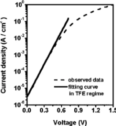
Figure 1 shows the typical semilog current density–
voltage共J–V兲 characteristics of Ni/p-GaN Schottky diodes
at 300 K. The fitting curve using the TFE model is also shown in Fig. 1. Yu et al.7indicated that the slope of ln I – V curves could not be analyzed using the thermionic emission
共TE兲 model, due to the carrier transport with a tunnel
com-ponent. In addition, these reports13,14 provide theoretical analysis of current tunneling through a Schottky barrier
共qB兲. The J–V characteristic in the presence of tunneling
can be described by the relation13,14
a兲
Electronic mail: [email protected]
FIG. 1. J – V curve of Ni/ p-GaN Schottky diodes under forward bias con-dition at 300 K and the fitting curve to the J – V characteristic in the TFE regime.
APPLIED PHYSICS LETTERS 86, 122109共2005兲
0003-6951/2005/86共12兲/122109/3/$22.50 86, 122109-1 © 2005 American Institute of Physics
J = J0exp共qV/E0兲, 共1兲 E0= E00coth共E00/kT兲, 共2兲 J0= A*T关E00q共B− V −兲兴0.5 k cosh共E00/kT兲 exp
冋
− q kT − q E0共B−兲册
, 共3兲 E00=共qh/4兲共N/m*兲0.5, 共4兲where J is the observed current density of Schottky diodes under forward bias condition, m*共m*= 0.6m
0, m0is the mass
of hole at rest兲15is the hole effective mass, 共=9.50,0is the permittivity in vacuum兲16 is the dielectric constant of GaN, A*共A*= 103.8 A / cm2K2兲17is the effective Richardson constant of p-GaN, h is Planck’s constant, V is voltage, q is the electron charge, N is the doping concentration, and is equal to共EF− EV兲/q. EV is the valence band maximum and
EF is the position of the Fermi level. was assumed to be
equal to 0.1 V in this study. According to the fitting J versus
V curve of samples using Eqs.共1兲–共3兲, the value of E0, E00,
and qB can be calculated to be 66 meV, 65 meV, and
1.8 eV, respectively. Then, the calculated value 共⬃7
⫻1019cm−3兲 of N using Eq. 共4兲 is similar to 关Mg兴, which
indicated that the tunneling current under forward bias
con-ditions took place because of the high Mg doping 关or the
deep level defect 共DLD兲 band induced by high Mg
doping兴.18,19 Kwak et al.18 have suggested that the current transport at the metal/high Mg doped p-GaN interface was dominated by a DLD band which was induced by high Mg doping. Kwak et al.19have also suggested that the DLD band had a large density defect, over 1019cm−3 size, existing in the p-GaN films and that the density of the DLDs increased as关Mg兴 increased. In addition, Shiojima et al.20 have found carrier capture and emission from acceptor-like DLDs for Ni/ p-GaN Schottky diodes. Further, it is worth noting that the calculated value of E00/ kT is slightly larger than 1, which
implies the current transport processes a tunnel component.14 On the other hand, the observed current is too small to obtain the fitting parameters for the J – V characteristic in the field
emission共FE兲 regime for Ni/p-GaN. This suggests that the
FE model cannot be used to study the qBof Ni/ p-GaN in
this case. In addition, the E00of 65 meV is not much greater
than kT 共kT=26 meV, at 300 K兲, so the FE will not take
place.13The effective resistance of the Schottky barrier in the FE regime is quite low, so the FE model is often used for ohmic contact.13
Figure 2 shows the typical semilog J – V characteristics of Ni/ p-GaN Schottky diodes at 350 and 400 K, respec-tively. The fitting curves using the TFE model are also shown in Fig. 2. We find that the barrier heights can readily be obtained by fitting the J – V curves using Eqs.共1兲–共3兲. From the TFE theory, a linear fit to the data for the J – V
measure-ments at 350 K yields E0= 67 meV and qB= 1.8 eV,
whereas a linear fit to the data for the J – V measurements at 400 K yields E0= 68 meV and qB= 1.8 eV. Both values for
the Schottky barrier height are in good agreement with the value calculated for J – V measurements at 300 K. These re-sults indicate that a TFE model can quantitatively explain the observed large forward leakage currents due to the existence of the induced high density of the acceptor-type DLDs by
high Mg doping. We conclude that the creation of a large number of DLDs in p-GaN leads to the reduction of the depletion layer width in the p-GaN near the interface, an increase in the probability of the TFE, and gives rise to large forward leakage. Consequently, the forward current transport with a tunnel component is not analyzed using the TE model. In order to further confirm whether the barrier-height value of Ni/ p-GaN Schottky diodes is 1.8 eV or not, XPS is used to study the surface Fermi level position within the band gap for Ni overlayer on p-GaN. XPS measurements
were performed using a monochromatic Al K␣ x-ray source.
The barrier height was determined from the XPS data using the following relation.21,22This equation was previously em-ployed by Tracy et al.23 for the calculation of the barrier heights共qn兲 of metals on n-GaN:
qn= EG− Eiv +共Ecore i − E core m 兲 = E G−共Ecore m − E VC兲 共5兲
EGis the band gap of the semiconductor, Ecore
m
is the binding energy of the semiconductor core-level peak following metal deposition, Ecorei is the initial binding energy of the core-level peak, EVi is the initial binding energy of the EV of the
semi-conductor, and EVCis equal to共Ecore
i − E V
i兲. All binding
ener-gies are measured relative to the EF. For the calculation of
the barrier heights 共qp兲 of Ni/p-GaN, the equation is ex-pressed as
FIG. 2. Forward J – V characteristic of Ni/ p-GaN Schottky diodes as a function of temperature.
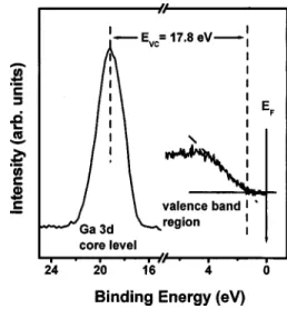
FIG. 3. The left-hand spectrum shows the Ga 3d core-level peak on
p-GaN without a Ni overlayer. The right-hand panel presents the spectrum
of the valence-band region. A linear fit is used to determine the energy of the valence-band edge.
122109-2 Yow-Jon Lin Appl. Phys. Lett. 86, 122109共2005兲
qp= Ecore Ni
− EVC 共6兲
where EcoreNi is the binding energy of the p-GaN core-level peak following Ni deposition.
Figure 3 shows an example of the Ga 3d core level and the valence-band spectrum collected on a p-GaN sample without a Ni overlayer. The EVCis calculated to be 17.8 eV.
This value is in good agreement with the value of 17.8 eV
reported by Hashizume et al.,24 Bermudez,25 Waldrop and
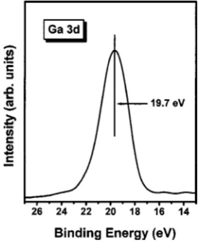
Grant,26and Wu and Kahn.27Figure 4 shows the Ga 3d core
level at the Ni/ p-GaN interface. The spectra determine the Ga 3d binding energy EcoreNi relative to the EF. In Fig. 4, we
can see that the EcoreNi is equal to 19.7 eV. Therefore, the qp
was calculated to be 1.9 eV, according to Eq.共6兲. This value is similar to the value of 1.8 eV obtained from J – V measure-ments. In addition, Rickert et al.28suggested that the barrier height value of the Ni/ p-GaN sample is approximately 1.9 eV, which supported our observed results from the XPS and J – V measurements.
In summary, the barrier height value of Ni/ p-GaN Schottky diodes was obtained from J – V measurements in this study. For Ni/ p-GaN Schottky diodes, the calculated barrier height value using the TFE model is in good agree-ment with the value of 1.9 eV obtained from x-ray photo-electron spectroscopy measurements. The induced DLD band through high Mg doping would lead to the reduction of the depletion layer width in the p-GaN near the interface, an increase in the probability of the TFE, and an increase in
current flow under forward bias conditions, which was not analyzed using the TE model.
This project is supported by National Science Council of Taiwan, Republic of China, under Contract No. NSC 93-2215-E-018-005. The XPS was kindly provided from the NTU Instrumentation Center at Taipei National Taiwan University.
1
O. Katz, V. Garber, B. Meyler, G. Bahir, and J. Salzman, Appl. Phys. Lett.
79, 1417共2001兲.
2
M. A. Khan, J. N. Kuznia, D. T. Olson, M. Blasingame, and A. R. Bhat-tarai, Appl. Phys. Lett. 63, 2455共1993兲.
3
M. A. Khan, J. N. Kuznia, A. R. Bhattarai, and D. T. Olson, Appl. Phys. Lett. 62, 1786共1993兲.
4
N. Biyikli, O. Aytur, I. Kimukin, T. Tut, and E. Ozbay, Appl. Phys. Lett.
81, 3272共2002兲.
5
M. W. Wang, J. O. McCaldin, J. F. Swenberg, T. C. McGill, and R. J. Hauenstein, Appl. Phys. Lett. 66, 1974共1995兲.
6
T. Mori, T. Kozawa, T. Ohwaki, Y. Taga, S. Naagai, S. Yamasaki, S. Asami, N. Shibata, and M. Koike, Appl. Phys. Lett. 69, 3537共1996兲. 7
L. S. Yu, D. Qiao, L. Jia, S. S. Lau, Y. Qi, and K. M. Lau, Appl. Phys. Lett. 79, 4536共2001兲.
8
X. A. Cao, S. J. Pearton, G. Dang, A. P. Zhang, F. Ren, and J. M. Van Hove, Appl. Phys. Lett. 75, 4130共1999兲.
9
P. J. Hartlieb, A. Roskowski, R. F. Davis, W. Platow, and R. J. Nemanich, J. Appl. Phys. 91, 732共2002兲.
10
D. L. Hibbard, R. W. Chuang, Y. S. Zhao, C. L. Jensen, H. P. Lee, Z. J. Dong, R. Shih, and M. Bremser, J. Electron. Mater. 29, 291共2000兲. 11
K. Shiojima, T. Sugahara, and S. Sakai, Appl. Phys. Lett. 74, 1936共1999兲. 12
J. K. Ho, C. S. Jong, C. N. Huang, C. C. Chiu, K. K. Shih, L. C. Chen, F. R. Chen, and J. J. Kai, J. Appl. Phys. 86, 4491共1999兲.
13
Michael Shur, Physics of Semiconductor Devices共Prentice-Hall, Engel-wood Cliffs, NJ, 1990兲.
14
H. Morkoç, Nitride Semiconductors and Devices共Springer, Berlin, 1999兲. 15
C. Merz, M. Kunzer, U. Kaufmann, I. Akasaki, and H. Amano, Semicond. Sci. Technol. 11, 712共1996兲.
16
M. Razeghi and A. Rogalski, J. Appl. Phys. 79, 7433共1996兲. 17
J. I. Pankove, S. Bloom, and G. Harbeke, RCA Rev. 36, 163共1975兲. 18
J. S. Kwak, O. H. Nam, and Y. Park, Appl. Phys. Lett. 80, 3554共2002兲. 19
J. S. Kwak, O. H. Nam, and Y. Park, J. Appl. Phys. 95, 5917共2004兲. 20
K. Shiojima, T. Sugahara, and S. Sakai, Appl. Phys. Lett. 77, 4353共2000兲. 21
J. R. Waldrop and R. W. Grant, Appl. Phys. Lett. 52, 1794共1988兲. 22
J. R. Waldrop and R. W. Grant, Appl. Phys. Lett. 62, 2685共1993兲. 23
K. M. Tracy, P. J. Hartlieb, S. Einfeldt, F. Davis, E. H. Hurt, and R. J. Nemanich, J. Appl. Phys. 94, 3939共2003兲.
24
T. Hashizume, S. Ootomo, S. Oyama, M. Konishi, and H. Hasegawa, J. Vac. Sci. Technol. B 19, 1675共2001兲.
25
V. M. Bermudez, J. Appl. Phys. 80, 1190共1996兲. 26
J. R. Waldrop and R. W. Grant, Appl. Phys. Lett. 68, 2879共1996兲. 27
C. I. Wu and A. Kahn, J. Appl. Phys. 86, 3209共1999兲. 28
K. A. Rickert, A. B. Ellis, J. K. Kim, J. L. Lee, F. J. Himpsel, F. Dwikusuma, and T. F. Kuech, J. Appl. Phys. 92, 6671共2002兲.
FIG. 4. Ga 3d core level at the Ni/ p-GaN interface. The binding energy is referenced to the Fermi level.
122109-3 Yow-Jon Lin Appl. Phys. Lett. 86, 122109共2005兲
Effect of reactive ion etching-induced defects on the surface band bending
of heavily Mg-doped
p
-type GaN
Yow-Jon Lina兲and Yow-Lin Chu
Institute of Photonics, National Changhua University of Education, Changhua 500, Taiwan, Republic of China
共Received 16 August 2004; accepted 25 February 2005; published online 29 April 2005兲
The effect of reactive ion etching-induced defects on the surface band bending of heavily Mg-doped
p-type GaN共p-GaN兲 was investigated in this study. According to the observed results from x-ray
photoelectron spectroscopy and secondary-ion-mass spectroscopy共SIMS兲 measurements, we found
that the formation of more nitrogen-vacancy-related defects created near the surface by reactive ion etching technique would lead to an increase in the surface band bending, a shift of the surface Fermi level toward the conduction-band edge, the reduction of the current flow at the metal/etched p -GaN interface, and an increase in the barrier height at the metal/etched p-GaN interface. In addition, from the SIMS measurements, it is suggested that the depth of the nitrogen-deficient near-surface region resulting from the dry-etch process is about 60 nm. © 2005 American Institute
of Physics.关DOI: 10.1063/1.1894580兴
I. INTRODUCTION
The recent progress in GaN-based optoelectronic
de-vices, such as blue light-emitting diodes 共LEDs兲 and laser
diodes共LDs兲,1–3points to the need of a deeper understanding of the optical and electrical characteristics of Mg-doped
p-type GaN共p-GaN兲. An important area in dry etching is the
characterization of damage which is produced in the semi-conductor through the bombardment of energetic ions. This induced damage, which may exist as vacancy complexes, dislocations, and recombination centers, can degrade the op-tical and electrical performances of devices. However, very little work has been done in investigating dry etch-induced defects in respect to heavily Mg-doped p-GaN. In this ar-ticle, we report the findings from a study of the effect of reactive ion etching-induced defects on the electrical proper-ties of heavily Mg-doped p-GaN. We find that according to the observed result from x-ray photoelectron spectroscopy
共XPS兲 and secondary-ion-mass spectroscopy 共SIMS兲
mea-surements, the nitrogen-vacancy-related defects induced by the reactive ion etching 共RIE兲 technique will lead to an in-crease in surface band bending and a shift of the surface Fermi level toward the conduction-band edge. In addition, from the SIMS measurements, it is suggested that the depth of the nitrogen-deficient near-surface region resulting from a dry-etch process is about 60 nm. Upon p-type doping, the changed donor defect formation energy will decrease in
tan-dem with the Fermi-level 共EF兲 position.
4,5
The nitrogen-vacancy-related defect is easily formed in the p-GaN films and the native defect of p-GaN.4According to the theoretical predictions,6 the only native defect with a relevant concen-tration in p-GaN is the nitrogen-vacancy-related defect.7As a result, we deduce that further nitrogen-vacancy-related de-fects may exist in the p-GaN near-surface region following etching. Another goal of this paper is to show that the RIE
represents a suitable technique choice for the fabrication of heavily Mg-doped p-GaN Schottky diodes with good quali-ties.
II. EXPERIMENTAL PROCEDURE
The epitaxial layers used in the experiments were grown on c-plane sapphire substrates using a metal-organic chemical-vapor deposition system. Trimethylgallium, ammo-nia, and biscyclopentadienylmagnesium were used as the Ga, N, and Mg sources, respectively. An undoped GaN buffer layer with a thickness of 650 nm was grown on the sapphire substrate at 520 ° C, followed by the growth of a Mg-doped
GaN layer共762 nm,3.6⫻1017cm−3兲 at 1100 °C. The grown
samples were annealed for the purpose of generating holes,
at 750 ° C for 30 min in N2 ambient. The Mg concentration
共关Mg兴兲 was 6⫻1019cm−3 for all samples. The关Mg兴 in
Mg-doped GaN was measured using SIMS. The samples were cleaned in chemical clean solutions of trichloroethylene, ac-etone, and methanol共referred to as as-cleaned p-GaN兲. Then, some of the as-cleaned samples were etched using the RIE
technique in BCl3plasma with a rf power of 150 W. During
the etching process, the BCl3flow rate was 5 SCCM
共stan-dard cubic centimeter per minute兲 and the chamber pressure
was 4 Pa. The etched depth is 100 nm. The etched sample was referred to as etched p-GaN. The as-cleaned and etched samples were then inserted into the vacuum chamber of a
ESCA PHI 1600 system. We took a Au 4f7/2peak and a Cu
2p3/2peak for energy reference purposes.
III. EXPERIMENTAL RESULTS AND DISCUSSION
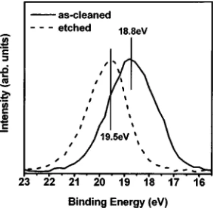
Figure 1 shows the Ga 3d core-level XPS spectra on the as-cleaned and etched p-GaN surfaces. We found that the Ga 3d core-level spectra of the etched sample shift toward the high binding-energy side, compared with that of the as-cleaned one. This indicated that the Ga 3d core-level spectra of the as-cleaned sample after etching treatment underwent a
a兲Author to whom correspondence should be addressed; electronic mail:
JOURNAL OF APPLIED PHYSICS 97, 104904共2005兲
0021-8979/2005/97共10兲/104904/4/$22.50 97, 104904-1 © 2005 American Institute of Physics
shift of 0.7 eV, and that the etching treatment gave rise to a shift of the surface Fermi level toward the conduction-band edge, resulting in an increase in the surface band bending.8,9 In Fig. 1, we also found that the full width at half maximum in the Ga 3d spectra of as-cleaned p-GaN is slightly larger than that of etched p-GaN. This may be due to that the fact that the contaminant and residual oxides on the p-GaN sur-face were removed during the etching process.
Figure 2 shows the XPS spectra of the as-cleaned and etched p-GaN surface near the valence-band edge region.
The valence-band maximum共VBM兲 is defined in a standard
way by the linear extrapolation of the low binding-energy edge of the valence-band spectrum. In Fig. 2, we can see that the VBM of the as-cleaned and etched samples is found at 1.0 and 1.7 eV below the EF, respectively. In addition, for
the as-cleaned or etched samples, the binding energy of the
Ga 3d core level 共18.8 eV for the as-cleaned sample and
19.5 eV for the etched sample, as shown in Fig. 1兲 with
respect to the VBM is 17.8 eV, which is in good agreement with previous results.10,11
To investigate the characteristics of defects induced by RIE technique, the as-cleaned and etched p-GaN surfaces were measured using XPS quantitative analysis. The relative Ga/ N atomic concentration ratio was determined from the integration of Ga 3d and N 1s peaks. In this work, the exact sensitivity factor for p-GaN was not known, so the Ga/ N ratio on the as-cleaned p-GaN surface was taken as 1. Con-sequently, the Ga/ N ratio on the etched p-GaN surface was calculated to be 1.5. XPS surface analysis revealed a lower
nitrogen atomic concentration on the etched sample. This indicates that the RIE technique may create more nitrogen vacancies on the sub-p-GaN surface. The
nitrogen-vacancy-related defect level above the EF, which is near the
conduction-band edge,12,13 will ionize and the
nitrogen-vacancy-related defects will become the dominant positively charged donors in the etched sample. For the preservation of the charge neutrality on the etched p-GaN surface, an in-crease in the positive charge for the extrinsic nitrogen-vacancy defects will lead to an increase in the negative charge in the surface space-charge region, an increase in the surface band bending, and a shift of the surface Fermi level toward the conduction-band edge. On the other hand, it has been shown that reactive ion etching n-type GaN surface improves the contact resistance,14which can be attributed to the formation of extrinsic donor-type nitrogen-vacancy-related defects. The suggestion is consistent with the above result of XPS analysis. Besides, we found that the reduction of the surface state, related to nitrogen-vacancy defects on the p-GaN surface, led to a reduction in the surface band bending by 0.25 eV in a previous study.15 In contrast, more nitrogen-vacancy-related defects created near the surface by the RIE technique will lead to an increase in the surface band bending of p-GaN.
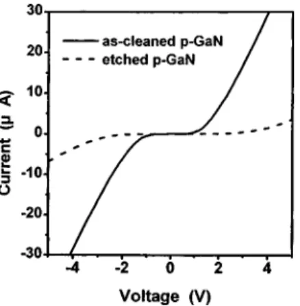
Figure 3 shows the depth profiles of Ga/ N ratios of as-cleaned p-GaN and etched p-GaN, respectively. The inten-sity of Ga SIMS divided by that of N SIMS equals the Ga/ N ratio. In Fig. 3, we find that the Ga/ N ratio of etched samples is larger than that of as-cleaned samples in the near-surface region. This implies that more nitrogen-vacancy-related de-fects were formed in the etched p-GaN films. We also find that the depth of the nitrogen-deficient near-surface region resulting from a dry-etch process is about 60 nm. The value is in good agreement with the value of 40– 60 nm reported by Cao et al.16 and Kent et al.17
Figure 4 shows the current–voltage共I–V兲 characteristics
of Ni/ Au 共20/20 nm, deposition used an electron-beam
evaporator兲 contacts on as-cleaned and etched p-GaN. The
gap spacing of the Ni/ Au metals pads is 25m. These I – V characteristics were observed using the transmission line
method共TLM兲. The fabrication process of the TLM pattern
has been reported previously.18 The I – V characteristics of
FIG. 1. Ga 3d core-level XPS spectra of as-cleaned and etched p-GaN.
FIG. 2. XPS spectra of the as-cleaned and etched p-GaN surface near the valence-band edge region.
FIG. 3. Depth profiles of Ga/ N ratios of the as-cleaned and etched p-GaN samples.
104904-2 Y. Lin and Y. Chu J. Appl. Phys. 97, 104904共2005兲
the TLM patterns were measured using a Keithley Model-4200-SCS/F semiconductor characterization system. Com-paring the I – V curves shown in Fig. 4, the I – V curve for the as-cleaned sample is better than that of the etched sample. In addition, the I – V curve for the as-cleaned sample, with a smaller turn on voltage and larger slope, is superior to that of the etched sample. The worse performance of the etched samples is attributable to the formation of the higher barrier between the Ni/ Au and p-GaN and an increase in the nitrogen-vacancy-related defects, suppressing an effect of the acceptorlike deep level defects19共DLDs兲 on the carrier trans-port at the Ni/heavily Mg-doped GaN interfaces, as well as the reduction of the hole concentration and the probability of the tunneling transmission through the DLD band for holes at the metal/ p-GaN interface.19,20The explanation for this is given later. Besides, in Figs. 1 and 2, we can see that the downward surface band bending of the etched samples in-deed increases. This indirectly implies that an increase in the surface band bending can lead to the degradation in the I – V characteristics of the etched sample. In this regard, the dry etching technique can be applied in the fabrication process of
p-GaN Schottky diodes, because more
nitrogen-vacancy-related defects formed below the p-GaN surface lead to an increased Schottky barrier for the transport of holes.
For Schottky diodes, secure ohmic contacts help to ob-tain the actual Schottky characteristics. Kwak et al. sug-gested that high Mg doping would lead to the formation of secure ohmic contacts of metals/ p-GaN.19In order to obtain the good qualities of p-GaN Schottky diodes, the heavily Mg-doped p-GaN has to be used to form the low-resistivity ohmic contact. Nevertheless, Kwak et al. found that the cur-rent transport at the metal/high Mg-doped p-GaN interface was dominated by a deep level defect band which was
in-duced by high Mg doping.19Kwak et al. suggested that the
DLD band possesses a large defect density over 1019cm−3
existing in the p-GaN films, and that the density of the DLDs
was enlarged as 关Mg兴 increased.20 In addition, Shiojima et
al.21 found carrier capture and emission from acceptorlike
DLDs for Ni/ p-GaN Schottky diodes. According to these results reported by Kwak et al. and Shiojima et al.,19–21 we deduced that the heavily Mg-doped p-GaN used to fabricate the Schottky diodes might lead to the formation of the low barrier height and a larger leakage of current at the Schottky
metals/ p-GaN interface. On the basis of this evidence, we concluded that the regions of Schottky contacts of high Mg-doped p-GaN could be etched by the RIE technique after the formation of good ohmic contacts, and more nitrogen-vacancy-related defects were produced in p-GaN near the surface, suppressing an effect of the acceptorlike DLDs on
p-GaN Schottky diodes. Therefore, following the deposition
of metals on the etched Schottky contacts of heavily Mg-doped p-GaN samples, we expect that the higher barrier height and smaller leakage current will be easily obtained. This will be further investigated in the future. Finally, we predict that the application of the RIE technique in the fab-rication of p-GaN Schottky diodes will result in the forma-tion of a high barrier height and a smaller leakage of current at the interfaces.
IV. CONCLUSIONS
In summary, the effect of defects created by the RIE technique on the electrical properties of heavily Mg-doped
p-GaN has been investigated. We found that the formation of
more nitrogen-vacancy-related defects created near the sur-face by the RIE technique would lead to an increase in the downward band bending. This indicates that the etching treatment gives rise to a shift of the surface Fermi level to-ward the conduction-band edge, which is in good agreement with the observed result from the measurements of the valence-band spectrum. Dry etching could be useful for the formation of the high barrier height and the low leakage of current at the metals/heavily Mg-doped p-GaN interface. This fact offers hope for the application of the RIE technique in the fabrication process of heavily Mg-doped p-GaN Schottky diodes with good qualities. We plan to experimen-tally fabricate such Schottky diodes in the near future.
ACKNOWLEDGMENT
This project is supported by National Science Council of Taiwan, Republic of China, under Contract No. NSC 93-2215-E-018-005.
1
M. Osiński, Gallium-Nitride-based Technologies 共SPIE, Washington, 2002兲.
2
S. J. Pearton, J. C. Zolper, R. J. Shul, and F. Ren, J. Appl. Phys. 86, 1 共1999兲.
3
H. Morkoç, Nitride Semiconductors and Devices共Springer, Berlin, 1999兲. 4
J. Neugebauer and C. G. Van de Walle, Phys. Rev. B 50, 8067共1994兲. 5
S. G. Lee and K. J. Chang, Semicond. Sci. Technol. 14, 138共1999兲. 6
J. Neugebauer and C. G. Van de Walle, Mater. Res. Soc. Symp. Proc. 395, 645共1996兲.
7
U. Kaufmann, M. Kunzer, M. Maier, H. Obloh, A. Ramakrishnan, B. Santic, and P. Schlotter, Appl. Phys. Lett. 72, 1326共1998兲.
8
K. A. Rickert, A. B. Ellis, F. J. Himpsel, J. Sun, and T. F. Kuech, Appl. Phys. Lett. 80, 204共2002兲.
9
G. Landgren, R. Ludeke, Y. Jugnet, J. F. Morar, and F. J. Himpsel, J. Vac. Sci. Technol. B 2, 351共1984兲.
10
C. I. Wu and A. Kahn, J. Appl. Phys. 86, 3209共1999兲. 11
T. Hashizume, S. Ootomo, S. Oyama, M. Konishi, and H. Hasegawa, J. Vac. Sci. Technol. B 19, 1675共2001兲.
12
C. G. Van de Walle, in Properties of Gallium Nitride and Related
Semi-conductors, edited by J. H. Edger, S. Strite, I. Akasaki, H. Amano, and C.
Wetzel共INSPEC, London, 1999兲, p. 275. 13
T. L. Tansley and R. J. Egan, Phys. Rev. B 45, 10942共1992兲. 14
Z. Fan, S. N. Mohammad, W. Kim, O. Aktas, A. E. Botchkarev, and H. Morkoç, Appl. Phys. Lett. 68, 1672共1996兲.
FIG. 4. I – V characteristics of Ni/ Au contacts on as-cleaned and etched
p-GaN.
104904-3 Y. Lin and Y. Chu J. Appl. Phys. 97, 104904共2005兲
15
Y. J. Lin, Z. L. Wang, and H. C. Chang, Appl. Phys. Lett. 81, 5183 共2002兲.
16
X. A. Cao et al., MRS Internet J. Nitride Semicond. Res. 5S1, W10.8 共2000兲.
17
D. G. Kent et al., Solid-State Electron. 45, 467共2001兲.
18
Y. J. Lin, Z. D. Li, C. W. Hsu, F. T. Chien, C. T. Lee, S. T. Shao, and H. C. Chang, Appl. Phys. Lett. 82, 2817共2003兲.
19
J. S. Kwak, O. H. Nam, and Y. Park, Appl. Phys. Lett. 80, 3554共2002兲. 20
J. S. Kwak, O. H. Nam, and Y. Park, J. Appl. Phys. 95, 5917共2004兲. 21
K. Shiojima, T. Sugahara, and S. Sakai, Appl. Phys. Lett. 77, 4353共2000兲.
104904-4 Y. Lin and Y. Chu J. Appl. Phys. 97, 104904共2005兲
Optical and electrical properties of heavily Mg-doped GaN
upon
„
NH
4…
2S
xtreatment
Yow-Jon Lina兲 and Yow-Lin Chu
Institute of Photonics, National Changhua University of Education, Changhua 500, Taiwan, Republic of China
Y. S. Huang
Department of Electronic Engineering, National Taiwan University of Science and Technology, Taipei 106, Taiwan, Republic of China
Hsing-Cheng Chang
Department of Automatic Control Engineering, Feng Chia University, Taichung 407, Taiwan, Republic of China
共Received 12 January 2005; accepted 29 March 2005; published online 10 May 2005兲
We have employed the photoluminescence 共PL兲 and surface photovoltage spectroscopy 共SPS兲
measurements to study the effects of共NH4兲2Sxtreatment on the optical and electrical properties of
p-type GaN共p-GaN兲 in this study. From the PL and SPS measurements, it is suggested that the 共MgGa–VN兲2+ 共MgGa:Ga vacancies occupied by Mg; VN:nitrogen vacancies兲 complexes near the p-GaN surface region were transformed into the 共MgGa-SN兲0 共SN:N vacancies occupied by S兲
complexes after共NH4兲2Sxtreatment, which resulted in the reduction of the ⬃2.8-eV PL intensity
and the increase of the hole concentration near the p-GaN surface region. © 2005 American
Institute of Physics. 关DOI: 10.1063/1.1926404兴
In recent years, GaN-related wide band gap semiconduc-tors have become the materials of choice for the fabrication of light emitting diodes operating in the green, blue, and violet regions of the visible spectrum.1,2The fabrication of high-quality ohmic contacts on n- and p-type GaN is essen-tial for improving the performance of optoelectronic devices.
However, ohmic contact formation to p-type GaN 共p-GaN兲
alloyed has been difficult to realize due to the absence of metals having a work function larger than that of p-GaN and the absence of p-GaN having a higher hole concentration. Recently, several groups have employed共NH4兲2Sxtreatment
which was designed to improve the electrical properties of
ohmic contacts to p-GaN.3–5 Lee et al. suggested that the
reduction of contact resistivity is due to direct contact of Pt on the clean p-GaN surface, via shift of barrier height for holes at the Pt/p-GaN interface.3 Jang and Seong have indi-cated that surface treatment led to an increase in the hole concentration of p-GaN and the occurrence probability of the field emission for holes at the Pt/p-GaN interface.4However, the effect of 共NH4兲2Sx treatment on optical properties of
p-GaN has not been investigated further. To date, the
rela-tionship between the optical and electrical properties of
p-GaN with surface treatment has also not yet been well
understood. For this study, we demonstrate that 共NH4兲2Sx
treatment results in the reduction of⬃2.8-eV
photolumines-cence共PL兲 intensity of the heavily Mg-doped p-GaN sample.
We deduce that the共MgGa–VN兲2+ 共MgGa: Ga vacancies
oc-cupied by Mg, VN: nitrogen vacancies兲 complexes near the
p-GaN surface region were transformed into the 共MgGa
-SN兲0 共SN : N vacancies occupied by S兲 complexes after
共NH4兲2Sxtreatment, which led to the reduction of donor-type
VN-related states near the surface region and an increase in
the hole concentration.4 This can explain why 共NH4兲2Sx
treatment is useful for the improvement of the electrical properties of ohmic contacts to p-GaN.
The epitaxial layers used in the experiments were grown on c-plane sapphire substrates using a metal-organic chemi-cal vapor deposition system. Trimethylgallium, ammonia and bis-cyclopentadienylmagnesium were used as the Ga, N, and Mg sources, respectively. An undoped GaN buffer layer with a thickness of 650 nm was grown on the sapphire substrate at 520 °C, followed by the growth of Mg-doped GaN layer
共762 nm, Mg concentration =6⫻1019cm−3兲 at 1100 °C. The
grown samples were annealed for the purpose of generating holes, at 750 °C for 30 min in N2ambient. The samples were
cleaned in chemical clean solutions of trichloroethylene,
acetone, and methanol 共referred to as as-cleaned p-GaN兲.
Then, some of the as-cleaned samples were dipped into a
共NH4兲2Sx solution 共S=6%兲 at 60 °C for 30 min 关referred
to as 共NH4兲2Sx-treated p-GaN兴. The as-cleaned and
共NH4兲2Sx-treated samples were then measured via PL and
surface photovoltage spectroscopy共SPS兲. The SPS
measure-ments, which used normalized incident light intensity,6were performed at normal incidence using a fixed grid and probe light chopped at 200 Hz. SPS is a powerful tool for the investigation of surface electronic structure, which has proven to be an extensive source of information about opti-cally active surface states at clean and real surfaces of vari-ous semiconductors, as well as surface with monolayer coverage.7–9
Figure 1 shows the room-temperature PL spectrum of the as-cleaned p-GaN and共NH4兲2Sx-treated p-GaN, respectively.
Using a He–Cd laser as an excitation source, the ⬃2.8-eV
PL band was only observed for the all samples due to the
heavily Mg doped.10 According to the reported result by
Kaufmann et al.,11 we find that the generation of the
⬃2.8-eV PL band may be attributed to the MgGa and
MgGa–VNcomplexes. In Fig. 1, we find that the PL intensity
a兲Author to whom correspondence should be addressed; electronic mail:
APPLIED PHYSICS LETTERS 86, 202107共2005兲
0003-6951/2005/86共20兲/202107/3/$22.50 86, 202107-1 © 2005 American Institute of Physics
of the共NH4兲2Sx-treated p-GaN is lower than that of the as-cleaned p-GaN. An explanation for this will be given later.
Figure 2 shows the room-temperature surface photovolt-age 共SPV兲 spectra of the as-cleaned and 共NH4兲2Sx-treated
p-GaN samples, respectively. The slope changes indicated a
one gap state, whose position relative to the conduction band
minimum Ec 共valence band maximum Ev兲 can be deduced
from the position of the downward共upward兲 slope changes
in the spectra.12,13We can see that the upward slope change at⬃3.07 eV indicates population of a donor state, situated at
⬃3.07 eV above the Ev 关Ev+ 3.07 eV, denoted by D1 in
Fig. 2共a兲兴. This state is attributed to the 共MgGa–VN兲2+
complex.11,14 Kaufmann et al. have suggested that the
MgGa–VN complex may exist in the heavily Mg-doped
p-GaN layer.15The MgGa–VNcomplex which is double
do-nors resulted in the reduction of the hole concentration in the heavily Mg-doped p-GaN sample.15,16However, in Fig. 2共b兲, we did not find population of a donor state, situated at Ev + 3.07 eV. This suggests that共NH4兲2Sxtreatment resulted in
the removal of the donor-type共MgGa–VN兲2+complexes near
the p-GaN surface region. We deduce that that the
共MgGa–VN兲2+complexes near the p-GaN surface region were
transformed into the共MgGa–SN兲0 complexes after共NH4兲2Sx
treatment and the共MgGa–SN兲0 complex near the p-GaN
sur-face region prefers a neutrality charged state, which results in
the reduction of the observed ⬃2.8-eV PL intensity. Kim
et al. have suggested that the reduction of MgGa–VNled to
the reduction of the observed⬃2.8-eV PL intensity.16 In a previous report,17 we have demonstrated that the S atoms might occupy nitrogen-related vacancies near the
共NH4兲2Sx-treated p-GaN surface region. In addition, Oh
et al. have suggested that PL is sensitive to material
surface.18 Besides, we predict that the neutral 共MgGa–SN兲0
complex will not play the role of the compensating donor.
According to the reported results by Lee et al.,3 Jang and
Seong,4and Lee et al.,5we find that the current-voltage char-acteristic of the metals/共NH4兲2Sx-treated p-GaN sample is indeed better than that of the metals/as-cleaned p-GaN sample.5This indirectly implies that the formation the neu-tral 共MgGa–SN兲0 complexes near the p-GaN surface region
may lead to an increase in the hole concentration and the improvement in the electrical properties of the metals/
共NH4兲2Sx-treated p-GaN sample. A proof for this will be
given later. On the other hand, we can also see that the downward slope change at 2.9–3.0 eV indicates population of an acceptor state, situated at 0.4–0.5 eV above the Ev,
关denoted by A1 in Fig. 2共a兲兴. The acceptor state is attributed
to the contamination-induced surface state 共i.e., the native oxide or carbon-related contamination兲.19Hartlieb et al.19 in-dicated that the band of surface states may extend as far as 0.6 eV above the Ev, according to the reported results by Wu
and Kahn20and Bermudez.21However, the native oxide and
carbon-related contamination on the p-GaN surface could be effectively removed using共NH4兲2Sxtreatment.
22
As a result, we do not find population of the acceptor state for
共NH4兲2Sx-treated p-GaN关shown in Fig. 2共b兲兴.
Figure 3 shows the room-temperature SPV spectra in the higher photon-energy region. We find that the peak at 3.382 eV represents the band–to–band transition for as-cleaned
p-GaN关shown in Fig. 3共a兲兴. Similarly, we also find that the
peak at 3.396 eV represents the band–to–band transition for
共NH4兲2Sx-treated p-GaN 关shown in Fig. 3共b兲兴. The larger
band gap共Eg兲 of the 共NH4兲2Sx-treated sample than that of the
as-cleaned sample is found 共shown in Fig. 3兲, due to the
reduction of the gap state density during the 共NH4兲2Sx
treatment.23,24This band-gap shift 共⌬Eg兲 is associated with
the Burstein–Moss shift and this shift energy共E兲 can be writ-ten as25
FIG. 1. Room-temperature PL spectra of 共a兲 as-cleaned p-GaN and 共b兲 共NH4兲2Sx-treated p-GaN.
FIG. 2. Room-temperature SPV spectra of 共a兲 as-cleaned and 共b兲 共NH4兲2Sx-treated p-GaN.
FIG. 3. Room-temperature SPV spectra of 共a兲 as-cleaned and 共b兲 共NH4兲2Sx-treated p-GaN in the higher photon-energy region.
202107-2 Linet al. Appl. Phys. Lett. 86, 202107共2005兲
E = Eg− Ego= 2h2 2mr *
冉
3N 冊
2/3 , 共1兲where Eg is the transition energy gap of p-GaN, Ego is the
intrinsic band gap of p-GaN, h is Planck’s constant, N is the carrier concentration of p-GaN, and mr*is the reduced
effec-tive mass of p-GaN. It can be seen from Eq. 共1兲 that an
increases in E will lead to an increase in N. Kim et al. have indicated that the increase in band gap may be attributed to the increased carrier concentration and the increase in carrier concentration can be explained by the Burstein–Moss shift.26 Lo et al. have also suggested that the band-gap shifts were due to the Burstein–Moss shift, which is related to the carrier concentration.27On the basis of the evidence, we deduce that the共MgGa–VN兲2+ complexes near the p-GaN surface region
were transformed into the 共MgGa–SN兲0 complexes after
共NH4兲2Sx treatment, which led to an increase in the hole
concentration near the p-GaN surface region and the reduc-tion of the⬃2.8-eV PL intensity, which is in agreement with the reported results by Kim et al.16
In summary, the effects of 共NH4兲2Sx treatment on the
optical and electrical properties of the heavily Mg-doped
p-GaN sample were investigated. After共NH4兲2Sx treatment, the共MgGa–VN兲2+ complexes near the p-GaN surface region
were transformed into the neutral 共MgGa–SN兲0 complexes,
which led to the reduction of the donor-type states near the surface region, an increase in the hole concentration near the
surface region, and the reduction of the⬃2.8-eV PL
inten-sity. This could explain why共NH4兲2Sxtreatment is useful for
the improvement of the electrical properties of ohmic con-tacts to p-GaN.
This project is supported by National Science Council of Taiwan, Republic of China.
1
H. Morkoç, Nitride Semiconductors and Devices共Springer, Berlin, 1999兲. 2
S. Nakamura and S. F. Chichibu, Introduction to Nitride Semiconductor
Blue Lasers and Light Emitting Diodes共Taylor & Francis, London, 2000兲.
3
J. L. Lee, J. K. Kim, J. W. Lee, Y. J. Park, and T. Kim, Phys. Status Solidi A 176, 763共1999兲.
4
J. S. Jang and T. Y. Seong, Appl. Phys. Lett. 76, 2743共2000兲. 5
C. S. Lee, Y. J. Lin, and C. T. Lee, Appl. Phys. Lett. 79, 3815共2001兲. 6
L. Aigouy, F. H. Pollak, J. Petruzzello, and K. Shahzad, Solid State Com-mun. 102, 887共1997兲.
7
M. Leibovitch, L. Kronik, E. Fefer, and Y. Shapira, Phys. Rev. B 50, 1739 共1994兲.
8
Y. Rosenwaks, L. Burstein, Y. Shapira, and D. Huppert, Appl. Phys. Lett.
57, 458共1990兲.
9
J. Szuber, Appl. Surf. Sci. 55, 143共1992兲. 10
S. M. Jeong, H. W. Shim, H. S. Yoon, M. G. Cheong, R. J. Choi, E. K. Suh, and H. J. Lee, J. Appl. Phys. 91, 9711共2002兲.
11
U. Kaufmann, M. Kunzer, M. Maier, H. Obloh, A. Ramakrishnan, B. Santic, and P. Schlotter, Appl. Phys. Lett. 72, 1326共1998兲.
12
N. Kinrot and Y. Shapira, Phys. Rev. B 65, 245303共2002兲. 13
S. Kuźmiński, Vacuum 54, 189共1999兲. 14
M. A. Reshchikov, G.-C. Yi, and B. W. Wessels, Phys. Rev. B 59, 13176 共1999兲.
15
U. Kaufmann, P. Schlotter, H. Obloh, A. Ramakrishnan, K. Köhler, and M. Maier, Phys. Rev. B 62, 10867共2000兲.
16
S. W. Kim, J. M. Lee, C. Huh, N. M. Park, H. S. Kim, I. H. Lee, and S. J. Park, Appl. Phys. Lett. 76, 3079共2000兲.
17
Y. J. Lin, C. D. Tsai, Y. T. Lyu, and C. T. Lee, Appl. Phys. Lett. 77, 687 共2000兲.
18
E. Oh, B. Kim, H. Park, and Y. Park, Appl. Phys. Lett. 73, 1883共1998兲. 19
P. J. Hartlieb, A. Roskowski, R. F. Davis, W. Platow, and R. J. Nemanich, J. Appl. Phys. 91, 732共2002兲.
20
C. I. Wu and A. Kahn, J. Appl. Phys. 86, 3209共1999兲. 21
V. M. Bermudez, J. Appl. Phys. 80, 1190共1996兲. 22
J. K. Kim, J. L. Lee, J. W. Lee, Y. J. Park, and T. Kim, J. Vac. Sci. Technol. B 17, 497共1999兲.
23
W. Mönch, J. Vac. Sci. Technol. B 4, 1085共1986兲. 24
C. Tejedor, F. Flores, and E. Louis, J. Phys. C 10, 2163共1977兲. 25
S. Ray, R. Banerjee, N. Basu, A. K. Batabyal, and A. K. Barua, J. Appl. Phys. 54, 3497共1983兲.
26
H. Kim, A. Piqué, J. S. Horwitz, H. Mattoussi, H. Murata, Z. H. Kafafi, and D. B. Chrisey, Appl. Phys. Lett. 74, 3444共1999兲.
27
C. Y. Lo, C. L. Hsu, Q. X. Yu, H. Y. Lee, and C. T. Lee, J. Appl. Phys. 92, 274共2002兲.
202107-3 Linet al. Appl. Phys. Lett. 86, 202107共2005兲
Electrical properties of Ni/ Au and Au contacts on
p
-type GaN
Yow-Jon Lina)
Institute of Photonics, National Changhua University of Education, Changhua 500, Taiwan, Republic of China
(Received 3 August 2004; accepted 25 October 2004; published 28 December 2004)
The electrical properties of Ni/ Au and Au contacts on p-type GaN共p-GaN兲 were investigated in
this study. From the experimental result, it is suggested that the current–voltage characteristic of Au/ Ni/ p-GaN is better than that of Au/ p-GaN. The secondary-ion mass spectroscopy measurements revealed that hydrogen is effectively removed from the p-GaN layer by the existence of the Ni film. These results suggest that a Ni film of Au/ Ni/ p-GaN significantly enhances hydrogen desorption from the p-GaN film, which leads to an increase in the hole concentration, the occurrence of the tunneling transmission for holes at the interface, and the improvement of electrical
properties of Au/ Ni/ p-GaN. © 2005 American Vacuum Society. [DOI: 10.1116/1.1835312]
I. INTRODUCTION
GaN has drawn much interest as a promising material for the fabrication of optoelectronic devices because of the suc-cess in commercialization of blue light-emitting diodes.1–3 To date, the contact resistance is not low enough to be ap-plied for blue laser diode because there is no metal with a high work function comparable to that of p-GaN. In order to manufacture low-resistivity ohmic contacts, various contact
schemes have been investigated.4–16 In recent years, the
Au/ Ni/ p-GaN ohmic contacts annealed in air have been studied extensively because they provide low specific contact resistances and high transparency.7–16 Kim et al. concluded that the improvement of oxidized Ni/ Au contact properties is due mainly to the formation of an intermediate NiO layer, rather than to an enhancement in p-type activation.9Qiao et
al. indicated that the presence of oxygen during annealing
appears to increase the conductivity of the p-GaN.10Koide et
al. indicated that the reason for reduction of the contact
re-sistance by the oxygen gas addition was believed to be due to formation of the p-GaN epilayer with high hole concentra-tion, caused by removal of hydrogen atoms that bonded with Mg atoms.11Mistele et al. suggested that the layer structure of the Ni/ Au layers do not seem to be that important than the selection of the annealing gas.16 The previous studies7–16 were focused on the effect of annealing in a partial oxygen ambient on electrical properties of ohmic contacts to
p-GaN. To our knowledge, the formation mechanism of
ohmic contacts of Au/ Ni/ p-GaN annealed under nitrogen ambient and the effects of Ni film on electrical properties of Ni/ Au ohmic contacts to p-GaN have not yet been well un-derstood. In this study, we find that a Ni film plays an im-portant role in the formation of Ni/ Au ohmic contacts to
p-GaN. According to the experimental result, we deduce that
a Ni layer on p-GaN enhances the activation of the acceptor and improves the ohmic performance of Au/ Ni/ p-GaN.
II. EXPERIMENTAL PROCEDURES
The epitaxial layers used in the experiments were grown on c-plane sapphire substrates using a metalorganic chemical
vapor deposition system. Trimethylgallium, ammonia共NH3兲,
and bis-cyclopentadienylmagnesium were used as the Ga, N, and Mg sources, respectively. An undoped GaN buffer layer with a thickness of 650 nm was grown on the sapphire sub-strate at 520° C, followed by the growth of an p-GaN layer
共762 nm兲 at 1100°C. Mg concentration 共关Mg兴兲 was 9
⫻1019cm−3 for all samples. The关Mg兴 in p-GaN was
mea-sured using secondary-ion mass spectroscopy (SIMS). The
grown samples were annealed at 750° C for 30 min in nitro-gen ambient using a thermal annealing furnace for the pur-pose of generating holes.12 The specific contact resistance
was measured using the transmission line method(TLM) for
Ni/ Au or Au contacts to p-GaN. A Ni/ Au 共50/600 nm兲
metal mask was employed to form rectangular mesa regions
with dimensions of 100⫻100m2. A reactive ion etching
system was used with BCl3 gas to etch the p-GaN wafers.
The dimensions of the metal contact pads in the TLM pattern
was 100⫻100m2. The gap spacings between the contact
pads were designed to be 5, 10, 15, 25, 35, 50, and 60m.
After the removal of the metallic mask, the samples were cleaned in chemical cleaning solutions of trichloroethylene,
acetone, and methanol(as-cleaned p-GaN). The surfaces of
the as-cleaned p-GaN samples were treated with aqua regia for 10 min prior to respective deposition of the Ni/ Au
共20/20 nm兲 and Au 共40 nm兲 metals using an electron-beam
evaporator. Next, the contacts were treated in a rapid thermal
annealing furnace at 300° C for 1 min (or 2 min) under
ni-trogen ambient. The current–voltage共I–V兲 characteristics of the TLM patterns, before and after annealing, were measured using a Keithley Model-4200-SCS/F semiconductor param-eter analyzer.
III. EXPERIMENTAL RESULTS AND DISCUSSION
Figure 1 shows the respective I – V characteristics of Au/ Ni/ p-GaN and Au/ p-GaN, measured between metal
pads with a gap spacing of 25m. The Au/ Ni/ p-GaN
sample does not show a linear I – V behavior. The
a)Electronic mail: [email protected]
Au/ p-GaN sample does not also show a linear I – V curve. However, in Fig. 1, we find that the I – V characteristic of the Au/ Ni/ p-GaN sample is better than that of the Au/ p-GaN sample. On the other hand, Qiao et al. suggested that the Au
layer has a larger work function than the Ni layer.10 This
implies that the contact conductivity of the Au/ p-GaN sample may be higher than that of the Ni/p-GaN sample. This cannot explain why the I – V characteristic of the Au/ Ni/ p-GaN sample is better than that of the Au/ p-GaN sample. An explanation for this will be given later.
Figure 2 shows the respective I – V characteristics of the
annealed Au/ Ni/ p-GaN sample and the annealed
Au/ p-GaN sample, measured between metal pads with a gap
spacing of 25m. The Au/ p-GaN samples were annealed at
300° C for 1 min in nitrogen ambient. Some of the Au/ Ni/ p-GaN samples were annealed at 300° C for 1 min in
nitrogen ambient (1-min-annealed Au/Ni/ p-GaN sample).
Some of the Au/ Ni/ p-GaN samples were annealed at 300° C
for 2 min in nitrogen ambient (2-min-annealed Au/Ni/ p
-GaN sample). We find that the 1-min-annealed Au/Ni/ p
-GaN samples show an approximate linear I – V behavior with a specific contact resistance of 7.5⫻10−3⍀ cm2. Simi-larly, the 2-min-annealed Au/ Ni/ p-GaN samples also show an approximate linear I – V behavior with a specific contact resistance of 4.2⫻10−3 ⍀ cm2. On the other hand, we find
that the I – V curve of the annealed Au/ p-GaN sample is similar to that of the unannealed Au/ p-GaN sample. Accord-ing to the experimental result, it is suggested that a Ni film played an important role in the ohmic contact formation of Au/ Ni/ p-GaN.
In order to clarify the effects of the Ni film on electrical properties of the Au/ Ni/ p-GaN sample, we investigated the hydrogen content in the p-GaN film by SIMS measurements
(Cameca IMS-4f system). First, Au and Ni/Au were
depos-ited on all p-GaN surfaces. Next, these samples were
an-nealed at 300° C for 1 min (or 2 min) in nitrogen ambient.
To remove the Au 共Au/Ni兲 film, the annealed Au/p-GaN
共Au/Ni/p-GaN兲 samples were treated in aqua regia solution
for 10 min, rinsed in deionized water for 1 min, and dried by a nitrogen blower. Next, these samples were measured using
SIMS. Figure 3(a) shows the SIMS profile of hydrogen
con-tent for the as-cleaned p-GaN samples. Figure 3(b) shows
the SIMS profiles of hydrogen content of Au/ p-GaN
an-nealed at 300° C for 1 min. Figure 3(c) shows the SIMS
profiles of hydrogen content of Au/ Ni/ p-GaN annealed at
300° C for 1 min. Figure 3(d) shows the SIMS profiles of
hydrogen content of Au/ Ni/ p-GaN annealed at 300° C for 2 min. It is noteworthy that the hydrogen content of the
1-min-annealed(or 2-min-annealed) Au/Ni/ p-GaN samples
is lower than that of the annealed Au/ p-GaN sample or that of the as-cleaned p-GaN samples. This is in good agreement with the previous report17 that the Ni film significantly en-hances hydrogen desorption from the p-GaN film, which leads to an increase in the hole concentration and the im-provement of electrical properties of Au/ Ni/ p-GaN. As a result, the Ni film enhances activation of Mg acceptors as catalysts at low temperature, causing the improvement of the electrical properties of Au/ Ni/ p-GaN, as shown in Figs. 1 and 2. We also find that the I – V characteristic of the 2-min -annealed Au/ Ni/ p-GaN sample is better than that of the 1-min-annealed Au/ Ni/ p-GaN sample, because the hydro-gen content of the 2-min-annealed Au/ Ni/ p-GaN sample is lower than that of the 1-min-annealed Au/ Ni/ p-GaN sample, as shown in Figs. 2 and 3. On the other hand, Rick-ert et al. have indicated that the barrier-height value of
FIG. 1. Typical I – V curves of(a) Au/Ni/ p-GaN and (b) Au/ p-GaN before
annealing. FIG. 2. Typical I – V curves of1 min, (b) Au/ p-GaN annealed at 300°C for 1 min, and (c) Au/Ni/ p(a) Au/Ni/ p-GaN annealed at 300°C for -GaN annealed at 300° C for 2 min.
49 Yow-Jon Lin: Electrical properties of Ni/ Au and Au contacts 49
Au/ p-GaN or Ni/p-GaN is approximately equal to 1.9 eV.18 Yu et al. have indicated that the value of tunneling parameter
共E00兲 of unannealed Ni/p-GaN was calculated to be
0.056 eV.19The deduced value of E00 is likely to contain a
tunneling component.19 This indirectly suggests that the Ni film of Au/ Ni/ p-GaN absorbs hydrogen and enhances acti-vation of Mg acceptors, causing the occurrence of the tun-neling transmission for holes at the Ni/p-GaN interface. Con-sequently, we deduce that the selection of the Ni/ Au layers seems to be an important factor for improving the ohmic contacts of p-GaN.
In Fig. 3, we can also see that the hydrogen content of the annealed Au/ p-GaN sample is close to that of the as-cleaned
p-GaN sample. Nakamura et al. have indicated that the
low-resistivity p-GaN films were obtained by N2-ambient thermal
annealing above 700° C.20 Nakamura et al. also suggested
that almost no change in resistivity was observed when the
p-GaN sample was annealed between room temperature and
400° C.20 This implies that low-temperature activation of
p-GaN and low-temperature hydrogen desorption from the p-GaN film were difficult to achieve by the absence of Ni
film.
IV. SUMMARY
In this study, the I – V characteristics of Au/ Ni/ p-GaN and Au/ p-GaN, and the effects of Ni layer on contact resis-tivity of Au/ Ni/ p-GaN have been investigated. SIMS mea-surements have revealed that the Ni layer on p-GaN en-hances the activation of the acceptor, as well as the occurrence of the tunneling transmission for holes at the Ni/p-GaN interface, and improves the ohmic performance of Au/ Ni/ p-GaN. This is probably due to the catalytic effect of Ni for the hydrogen desorption.
ACKNOWLEDGMENTS
The author would like to thank the National Science Council of the Republic of China for financially supporting this research under Contract No. NSC 93-2215-E-018-005. The SIMS was kindly provided from the NTHU Instrumen-tation Center at Hsinchu National Tsing Hua University.
1
M. Osiński, Gallium-Nitride-Based Technologies (SPIE, Washington, 2002).
2
H. Morkoç, Nitride Semiconductors and Devices(Springer, Berlin, 1999). 3
E. F. Schubert, Light-Emitting Diodes(Cambridge University Press, Cam-bridge, 2003).
4
J. S. Kwak, O. H. Nam, and Y. Park, Appl. Phys. Lett. 80, 3554(2002). 5
H. W. Jong and J. L. Lee, J. Appl. Phys. 93, 5416(2003). 6
J. O. Song, D. S. Leem, J. S. Kwak, O. H. Nam, Y. Park, and T. Y. Seong, Appl. Phys. Lett. 83, 2372(2003).
7
Y. J. Lin, Z. D. Li, C. W. Hsu, F. T. Chien, C. T. Lee, S. T. Shao, and H. C. Chang, Appl. Phys. Lett. 82, 2817(2003).
8
J. S. Kwak, J. Cho, S. Chae, O. H. Nam, C. Sone, and Y. Park, Jpn. J. Appl. Phys., Part 1 40, 6221(2001).
9
H. Kim, D. J. Kim, S. J. Park, and H. Hwang, J. Appl. Phys. 89, 1506 (2001).
10
D. Qiao, L. S. Yu, S. S. Lau, J. Y. Lin, H. X. Jiang, and T. E. Haynes, J. Appl. Phys. 88, 4196(2000).
11
Y. Koide, T. Maeda, T. Kawakami, S. Fujita, T. Uemura, N. Shibata, and M. Murakami, J. Electron. Mater. 28, 341(1999).
12
J. K. Sheu, Y. K. Su, G. C. Chi, P. L. Koh, M. J. Jou, C. M. Chang, C. C. Liu, and W. C. Hung, Appl. Phys. Lett. 74, 2340(1999).
13
J. K. Ho, C. S. Jong, C. N. Huang, C. Y. Chen, C. C. Chiu, and K. K. Shih, Appl. Phys. Lett. 74, 1275(1999).
14
J. K. Ho, C. S. Jong, C. N. Huang, C. C. Chiu, K. K. Shih, L. C. Chen, F. R. Chen, and J. J. Kai, J. Appl. Phys. 86, 4491(1999).
15
S. H. Wang, S. E. Mohney, and R. Birkhahn, J. Appl. Phys. 91, 3711 (2002).
16
D. Mistele, F. Fedler, H. Klausing, T. Rotter, J. Stemmer, O. K. Semchi-nova, and J. Aderhold, J. Cryst. Growth 230, 564(2001).
17
I. Waki, H. Fujioka, M. Oshima, H. Miki, and A. Fukizawa, Appl. Phys. Lett. 78, 2899(2001).
18
K. A. Rickert, A. B. Ellis, J. K. Kim, J. L. Lee, F. J. Himpsel, F. Dwikusuma, and T. F. Kuech, J. Appl. Phys. 92, 6671(2002). 19
L. S. Yu, D. Qiao, L. Jia, S. S. Lau, Y. Qi, and K. M. Lau, Appl. Phys. Lett. 79, 4536(2001).
20
S. Nakamura, T. Mukai, M. Senoh, and N. Iwasa, Jpn. J. Appl. Phys., Part 2 31, L139(1992).
FIG. 3. SIMS profile of hydrogen content of (a) as-cleaned p-GaN, (b) Au/ p-GaN annealed at 300° C for 1 min,(c) Au/Ni/ p-GaN annealed at 300° C for 1 min, and(d) Au/Ni/ p-GaN annealed at 300°C for 2 min.
50 Yow-Jon Lin: Electrical properties of Ni/ Au and Au contacts 50
Reproduced with permission of the copyright owner. Further reproduction prohibited without permission.
Study of Schottky Barrier Heights of Indium-Tin-Oxide on p-GaN Using X-ray Ph...
Yow-Jon Lin; Chou-Wei Hsu
Journal of Electronic Materials; Sep 2004; 33, 9; ProQuest Science Journals pg. 1036