國 立 交 通 大 學
電信工程學系
碩 士 論 文
無線區域網路之 CMOS 鏡像拒斥低雜訊放大器、
超寬頻系統之電流再利用低雜訊放大器、
超寬頻系統之低功率高線性度無電感混頻器
之設計與研究
Design of CMOS Image-Rejection LNA for WLAN,
Current-Reused LNA for UWB, and Low-Power
High-Linearity Inductorless Mixer for UWB
研究生:魏廉昇
指導教授:周復芳 博士
無線區域網路之
CMOS 鏡像拒斥低雜訊放大器、
超寬頻系統之電流再利用低雜訊放大器、
超寬頻系統之低功率高線性度無電感混頻器
之設計與研究
Design of CMOS Image-Rejection LNA for WLAN,
Current-Reused LNA for UWB, and Low-Power High-Linearity
Inductorless Mixer for UWB
研究生:魏廉昇 Student: Lien-Sheng Wei
指導教授:周復芳 博士 Advisor: Dr. Christina F. Jou
國 立 交 通 大 學
電 信 工 程 學 系 碩 士 班
碩 士 論 文
A thesis
Submitted to Department of Communication Engineering College of Electrical and Computer Engineering
National Chiao Tung University In Partial Fulfillment of the Requirements
for the Degree of Master of Science in Communication Engineering
June 2008
無線區域網路之 CMOS 鏡像拒斥低雜訊放大器、
超寬頻系統之電流再利用低雜訊放大器、
超寬頻系統之低功率高線性度無電感混頻器
之設計與研究
研究生:魏廉昇 指導教授:周復芳 博士
國立交通大學電信工程學系碩士班
摘 要
本論文的第一部份探討具有鏡像拒斥功能之低功率低雜訊放大器應用於 IEEE 802.11a,此電路設計一並聯電感電容槽於電流再利用架構的內部級來達成 鏡像拒斥的功能,鏡像拒斥濾波器的原理及品質因數 Q 強化技巧將被分析與介 紹,量測結果顯示此電路擁有令人滿意的效能與-27 dB 的鏡像拒斥能力。 在第二部份中將提出一超寬頻低雜訊放大器,此電路改善電阻並聯回授放大 器,將其電阻負載用 PMOS 替代。藉由堆疊兩顆電晶體並在其閘級與汲級間加 入回授電阻,此超寬頻低雜訊放大器能夠同時達到高增益與輸入端寬頻匹配,量 測結果顯示:優於-10 dB 之輸入與輸出端反射損耗、3.3 dB 之最小雜訊指數、14.1 dB 之平均增益並消耗 14.4 mW 之功率。 最後部份提出一低功率、高線性度、無電感混頻器應用於超寬頻通訊系統, 此混頻器利用共閘級放大器作為轉導級,使之較易達到寬頻輸入端匹配且不需要 電感,一些線性度改善技巧將被利用來增加IIP3,量測結果顯示:在 3.1 到 10.6 GHz 頻段其射頻端反射損耗大於-10 dB,在 100 MHz 中頻端反射損耗為-26 dB, 且達到3 到 8 dBm 之高線性度與 4.68 mW 之低功率消耗。Design of CMOS Image-Rejection LNA for WLAN,
Current-Reused LNA for UWB, and Low-Power
High-Linearity Inductorless Mixer for UWB
Student: Lien-Sheng Wei Advisor: Dr. Christina F. Jou
Department of Communication Engineering
National Chiao Tung University
ABSTRACT
In the first part of this thesis, a low-power low-noise amplifier (LNA) with image-rejection (IR) function is designed for IEEE 802.11a. It exploits a simple parallel LC tank in inter-stage of current-reused configuration to achieve IR function. The principles of IR filter will be analyzed and quality factor Q enhancement technique will be introduced. The measured results show the satisfied performances and IR ability of -27 dB.
In the second part, an ultra-wideband (UWB) LNA is proposed. It improves resistive shunt feedback amplifier to replace load resistor by a PMOS. By stacking two transistors and employing a feedback resistor to connect gate and drain, the proposed LNA can simultaneously achieve high gain and input impedance matching. The measured results reveal better than -10 dB input and output return loss, minimum noise figure of 3.3 dB, and average gain of 14.1 dB from consuming 14.4 mW power.
Finally, a low-power, high-linearity, and inductorless mixer for UWB communication is presented. The mixer adopts common-gate amplifier as
transconductance stage to easily achieve wideband matching without inductors. Some linearity-improvement techniques are exploited to increase the IIP3. The measured results express better than -10 dB RF port return loss in 3.1-10.6 GHz, IF port return loss of -26 dB at 100 MHz, high IIP3 of 3~8 dBm, and low power consumption of 4.68 mW.
誌謝
能夠完成這篇碩士論文,首先我要感謝我的指導老師周復芳教授,在這兩年 的碩士生涯給予我許多關心與指導,讓我在射頻積體電路設計這塊領域上有個好 的起步;也感謝論文口試委員郭建男教授以及胡樹教授的不吝指導,讓這篇論 文內容更清楚完善;另外也謝謝國家晶片中心給予晶片下線與量測的支援與協 助,我才能順利進行研究。 我也要感謝實驗室裡同伴們,實驗室的氣氛很好,我的兩年碩士生活既快樂 又充實。感謝我的同學沛遠、志豪、昱舜、智元,和你們一起做研究很愉快,可 以藉由互相討論問題,激勵出新的靈感想法;感謝學長姊俊緯、智鵬、宜星、匯 儀、哲揚、寶明,以及畢業的子豪、瑞嫻、宇清,在有問題的時候能幫助我討論 解惑,使我更快找出答案;也謝謝學弟子哲、玠瑝、昭維、宗廷、奕霖,有你們 陪伴讓實驗室更加熱鬧歡樂。 最後我要感謝我的父母、姊姊,以及我的女友純靈,謝謝你們在我求學之路 上的支持與鼓勵,使研究的路更為順遂,讓我能夠在這兩年順利完成碩士學位。 廉昇 於 2008 年 風城 夏Contents
Chinese Abstract ... I
English Abstract ... II
Acknowledgment ... IV
Contents ... V
List of Tables ... VII
List of Figures ... VIII
Chapter 1 Introduction ... - 1 -1.1 Background and motivation ... - 1 -
1.2 Thesis organization ... - 3 -
Chapter 2 Design of LNA with Image-Rejection Function for WLAN system ... - 4 -
2.1 Introduction ... - 4 -
2.2 Numerous topology of IR LNA ... - 5 -
2.3 Conventional current-reused amplifier ... - 9 -
2.4 Architecture ... - 10 -
2.5 Design considerations ... - 11 -
2.5.1 Input matching analysis ... - 11 -
2.5.2 Image-rejection filter analysis ... - 12 -
2.6 Chip implementation and measured results ... - 16 -
2.6.1 Measurement considerations ... - 16 -
2.6.2 Measured Results and discussion ... - 19 -
2.6.3 Comparison with other literatures ... - 25 -
Chapter 3 Design of Current-Reused LNA for UWB ... - 27 -
3.1 Introduction ... - 27 -
3.2 Numerous topology of wideband LNA ... - 27 -
3.3 Architecture ... - 30 -
3.4.1 Gain analysis ... - 32 -
3.4.2 Input matching analysis ... - 32 -
3.5 Chip implementation and measured results ... - 35 -
3.5.1 Layout considerations ... - 35 -
3.5.2 Measurement considerations ... - 36 -
3.5.3 Measured and simulated results ... - 40 -
3.5.4 Comparison with other literatures ... - 48 -
Chapter 4 Design of Low-Power High-Linearity Inductorless Mixer for UWB ... - 50 -
4.1 Introduction ... - 50 -
4.2 Architecture ... - 52 -
4.3 Design considerations ... - 53 -
4.3.1 Common-gate transconductance stage with source resistor ... - 53 -
4.3.2 Current-Injection Technique ... - 56 -
4.4 Chip implementation and measured results ... - 57 -
4.4.1 Measured considerations ... - 57 -
4.4.2 Measured Results and discussion ... - 62 -
4.4.3 Comparison with other literatures ... - 69 -
Chapter 5 Conclusion and Future Work ... - 71 -
5.1 Conclusion ... - 71 -
5.1.1 Design of LNA with IR function for WLAN system ... - 71 -
5.1.2 Design of current-reused LNA for UWB system ... - 72 -
5.1.3 Design of low-power high-linarity inductorless mixer for UWB system ... - 72 -
5.2 Future work ... - 73 -
References ... - 74 -
Vita ... ‐ 77 ‐
Publication Remarks ... ‐ 77 ‐
List of Tables
Table 2.1 Performance summary of the proposed IR LNA ... ‐ 25 ‐ Table 2.2 Comparison of the IR LNA performances ... ‐ 26 ‐ Table 3.1 Performance summary of the proposed LNA ... ‐ 48 ‐ Table 3.2 Comparison of Ultra Wide‐band LNA ... ‐ 49 ‐ Table 4.1 Performance summary of the proposed mixer ... ‐ 69 ‐ Table 4.2 Comparison of the UWB mixer ...‐ 70 ‐List of Figures
Fig. 1.1. DS‐UWB spectrum allocation. ... ‐ 2 ‐ Fig. 2.1. The IR LNA with the second‐order active notch filter. ... ‐ 6 ‐ Fig. 2.2. The IR LNA with the third‐order passive notch filter... ‐ 6 ‐ Fig. 2.3. The IR LNA with the third‐order active notch filter. ... ‐ 7 ‐ Fig. 2.4. The IR LNA with the forth‐order T structure filter. ... ‐ 8 ‐ Fig. 2.5. The IR LNA with active filter. ... ‐ 9 ‐ Fig. 2.6. Conventional current‐reused amplifier. ... ‐ 10 ‐ Fig. 2.7. Circuit schematic of the proposed IR LNA. ... ‐ 11 ‐ Fig. 2.8. The small signal equivalent circuit of input stage of the proposed LNA. ... ‐ 12 ‐ Fig. 2.9. Schematic of the IR filter. ... ‐ 13 ‐ Fig. 2.10. The small signal equivalent circuit looking into the gate of M2. ... ‐ 14 ‐ Fig. 2.11. Simulation result of Av =X Y/ in Fig. 2.7. ... ‐ 15 ‐ Fig. 2.12. Simulation result of the inter‐stage matching. ... ‐ 15 ‐ Fig. 2.13. On‐wafer measurement of proposed IR LNA ... ‐ 16 ‐ Fig. 2.14. Layout of the proposed LNA. ... ‐ 17 ‐ Fig. 2.15. Micrograph of the proposed LNA. ... ‐ 17 ‐ Fig. 2.16. Measurement setups for (a) S‐parameter. ... ‐ 18 ‐ Fig. 2.16. Measurement setups for (b) noise figure. ... ‐ 18 ‐ Fig. 2.16. Measurement setups for (c) P1dB. ... ‐ 18 ‐ Fig. 2.16. Measurement setups for (d) IIP3 ... ‐ 19 ‐ Fig. 2.17. Measured and simulated gain (S21). ... ‐ 21 ‐ Fig. 2.18. Measured and simulated input return loss (S11). ... ‐ 21 ‐ Fig. 2.19. Measured and simulated output return loss (S22). ... ‐ 22 ‐ Fig. 2.20. Measured and simulated isolation (S12). ... ‐ 22 ‐ Fig. 2.21. Measured and simulated noise figure (NF). ... ‐ 23 ‐ Fig. 2.22. Measured and simulated P1dB. ... ‐ 23 ‐ Fig. 2.23. Simulated IIP3. ... ‐ 24 ‐ Fig. 2.24. Measured IIP3. ... ‐ 24 ‐Fig. 3.1. Conventional wideband configurations. (a) Resistor‐terminated common‐source amplifier. (b) Common‐gate amplifier. (c) Resistive shunt‐feedback amplifier. ... ‐ 28 ‐
Fig. 3.2. Conventional distributed amplifier. ... ‐ 29 ‐
Fig. 3.3. The small signal equivalent circuit of CS amplifier with inductive source degeneration. .. ‐ 30 ‐
Fig. 3.4. Current‐reused amplifier. ... ‐ 30 ‐
Fig. 3.6. The small signal equivalent circuit of input stage. ... ‐ 33 ‐ Fig. 3.7. Simulated result of input reflection coefficient. ... ‐ 34 ‐ Fig. 3.8. Simulated result of output reflection coefficient ... ‐ 35 ‐ Fig. 3.9. Chip layout of the UWB LNA. ... ‐ 36 ‐ Fig. 3.10. Microphotograph of the UWB LNA with probes. ... ‐ 37 ‐ Fig. 3.11. On‐wafer measurement of UWB LNA test diagram. ... ‐ 37 ‐ Fig. 3.12. Measurement setups for (a) S‐parameter. ... ‐ 38 ‐ Fig. 3.12. Measurement setups for (b) noise figure. ... ‐ 38 ‐ Fig. 3.12. Measurement setups for (c) P1dB. ... ‐ 39 ‐ Fig. 3.12. Measurement setups for (d) IIP3. ... ‐ 39 ‐ Fig. 3.13. Measured and simulated results of S11. ... ‐ 41 ‐ Fig. 3.14. Measured and simulated results of S22. ... ‐ 41 ‐ Fig. 3.15. Measured and simulated results of S21. ... ‐ 42 ‐ Fig. 3.16. Measured and simulated results of S12. ... ‐ 42 ‐ Fig. 3.17. Measured and simulated results of noise figure. ... ‐ 43 ‐ Fig. 3.18. Measured and simulated results of P1dB at (a) 3.1 GHz. ... ‐ 44 ‐ Fig. 3.18. Measured and simulated results of P1dB at (b) 4.9 GHz. ... ‐ 44 ‐ Fig. 3.18. Measured and simulated results of P1dB at (c) 6.8GHz. ... ‐ 44 ‐ Fig. 3.18. Measured and simulated results of P1dB at (d) 8.7 GHz. ... ‐ 45 ‐ Fig. 3.18. Measured and simulated results of P1dB at (e) 10.6 GHz ... ‐ 45 ‐ Fig. 3.19. Measured result of IIP3 at (a) 3.1 GHz. ... ‐ 46 ‐ Fig. 3.19. Measured result of IIP3 at (b) 4.9 GHz. ... ‐ 46 ‐ Fig. 3.19. Measured result of IIP3 at (c) 6.8GHz. ... ‐ 46 ‐ Fig. 3.19. Measured result of IIP3 at (d) 8.7 GHz. ... ‐ 47 ‐ Fig. 3.19. Measured result of IIP3 at (e) 10.6 GHz. ... ‐ 47 ‐ Fig. 4.1 The mixer using the distributed matching network. ... ‐ 51 ‐ Fig. 4.2. The mixer using the LC ladder matching network. ... ‐ 51 ‐ Fig. 4.3. Schematic of the proposed mixer. ... ‐ 53 ‐ Fig. 4.4. CG amplifier. ... ‐ 54 ‐ Fig. 4.5. CS amplifier. ... ‐ 55 ‐ Fig. 4.6. Dynamic current‐injection technique. ... ‐ 57 ‐ Fig. 4.7. Layout of the proposed mixer. ... ‐ 58 ‐ Fig. 4.8. Micrograph of the proposed mixer. ... ‐ 58 ‐ Fig. 4.9. On‐wafer measurement of UWB LNA test diagram. ... ‐ 59 ‐ Fig. 4.10. Measurement setup of the proposed mixer for (a) RF port and IF port return loss. . ‐ 60 ‐ Fig. 4.10. Measurement setup of the proposed mixer for (b) conversion gain and P1dB. .. ‐ 60 ‐ Fig. 4.10. Measurement setup of the proposed mixer for (c) IIP3. ... ‐ 61 ‐ Fig. 4.10. Measurement setup of the proposed mixer for (d) noise figure ... ‐ 61 ‐
Fig. 4.11. Measured conversion gain versus LO power at (a) RF frequency of 3.1 GHz. ... ‐ 63 ‐ Fig. 4.11. Measured conversion gain versus LO power at (b) RF frequency of 6.6 GHz. ... ‐ 63 ‐ Fig. 4.11. Measured conversion gain versus LO power at (c) RF frequency of 10.6 GHz ... ‐ 63 ‐ Fig. 4.12. Measured and Simulated Conversion Gain of the proposed mixer. ... ‐ 64 ‐ Fig. 4.13. Measured and simulated RF port return loss. ... ‐ 64 ‐ Fig. 4.14. Measured and simulated P1dB at (a) RF frequency of 3.1 GHz. ... ‐ 65 ‐ Fig. 4.14. Measured and simulated P1dB at (b) RF frequency of 6.6 GHz. ... ‐ 65 ‐ Fig. 4.14. Measured and simulated P1dB at (c) RF frequency of 10.6 GHz. ... ‐ 65 ‐ Fig. 4.15. Measured IIP3 at (a) RF frequency of 3.1 GHz. (b) RF frequency of 4.9 GHz. ... ‐ 66 ‐ Fig. 4.15. Measured IIP3 at (c) RF frequency of 6.6 GHz. (d) RF frequency of 8.6 GHz. ... ‐ 66 ‐ Fig. 4.15. Measured IIP3 at (e) RF frequency of 10.6 GHz. ... ‐ 66 ‐ Fig. 4.16. Measured and simulated IIP3 with a fixed IF frequency of 100 MHz and LO power of ‐2.5 dBm. ... ‐ 67 ‐ Fig. 4.17. Measured and simulated double sideband noise figure. ... ‐ 67 ‐ Fig. 4.18. RF‐to‐LO isolation. ... ‐ 68 ‐ Fig. 4.19. LO‐to‐RF isolation... ‐ 68 ‐
Chapter 1
Introduction
1.1 Background and motivation
The IEEE 802.11a standard, which is based on orthogonal frequency division multiplexing (OFDM) modulation, provides nearly five times data rate and as much as ten times the overall system capacity as 802.11b wireless local area netwirk (WLAN) systems.
The low-noise amplifier (LNA) is the quite important block of front-end circuit in radio-frequency (RF) communication system, that's because the signal transmitted from antenna and amplified through the LNA immediately. The total noise figure of the receiver is dominated by the LNA. Thus the LNA is usually designed for low noise and high gain to suppress the noise of next stage. Recently, the most used architecture is heterodyne receiver. It has image problem which will cause the interferences to influence intermediate-frequency (IF). The image signal must be cancelled before the mixer. This thesis will discuss the LNA and image issue.
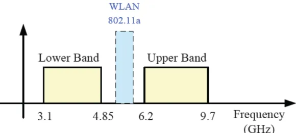
The Federal Communications Commission (FCC) has allocated 7500-MHz bandwidth for ultra-wideband (UWB) applications in the 3.1–10.6 GHz frequency range in 2002. This standard has capable of transmitting data over a wide spectrum of frequency bands with very low power and high data rates. Among the possible applications, UWB technology may be used for imaging systems, vehicular and ground-penetrating radars, and communication systems. In particular, it is envisioned to replace almost every cable at home or in an office with a wireless connection that features hundreds of megabits of data per second. Because UWB transmission spreads the energy of radio signals across an ultra wide bandwidth of up to 7.5GHz, its signal
level can be lower than the noise floor of traditional frequency-domain RF technologies. Hence, the chips for UWB consume lower power compared with other commonly used RF transceivers. Direct sequence code division multiple access (DS-CDMA) and multi-band orthogonal frequency division multiple access (MB-OFDM) are two mainly modulation technologies for UWB communications. Fig. 1.1 shows the reference spectral mask for DS-UWB scheme.
The RF transceiver for UWB system is an attractive research. This thesis will discuss the LNA and the mixer for UWB band. Both proposed circuits are designed for low power operation to satisfy the requirements of UWB standard.
1.2 Thesis
organization
We will discuss three circuits about LNA and mixer in this thesis. The chapter 2, chapter 3, and chapter 4 will introduce the proposed circuits. At first, we will make an introduction, present some previous researches, and indicate the advantages and drawbacks. Then we will propose the architecture and explain the circuit. The principles of the circuit and design considerations will be analyzed. The layout and measurement considerations will also be discussed. We will show the simulated and measured data and discuss the results. Finally, the performances will be listed in a table and compare with other literatures. The chapter 5 will make a conclusion and discuss the future work.
In chapter 2, a LNA with image-rejection (IR) function application for WLAN communication system will be expressed. The new design based on current-reused configuration will be presented. The principles of IR filter will be analyzed.
In chapter 3, a LNA for UWB system will be presented. By improving the resistive shunt feedback amplifier to current-reused amplifier, which stacking PMOS and NMOS, the input impedance can match to 50Ω over wide bandwidth and the gain will not reduce owing to the enhancement of transconductance. The details will be explained in chapter 3.
Chapter 4 will introduce a mixer for UWB system. The mixer adopts some techniques to improve the linearity, and it can achieve wideband input matching without the use of inductor. For UWB application, the mixer is also designed for low power operation.
Chapter 2
Design of LNA with Image-Rejection
Function for WLAN system
2.1 Introduction
The growing WLAN has generated increasing interest in technologies that will enable higher data rates and capacity than initially deployed systems. The 802.11a standard (5-6 GHz), released by IEEE in 1999, is based on OFDM modulation technology with data rates up to 54 Mbps in the 5 GHz band.
For RF integrated circuits wireless receivers, the need for low-power and low-cost systems demands the use of CMOS technology to arrive in a single chip solution. Heterodyne and homodyne are two major widely used receiver architectures in modern handsets. Each of the architectures has its own advantages and drawbacks. Homodyne architecture receiver, for instance, has higher level of integration due to its image-free architecture, but the DC offsets issues are the problems. By contrast, heterodyne architecture translate RF signal to IF through the mixer will deal with problem of image. The RF and image bands symmetrically located above and below the local-frequency (LO) are down-converted to the same center frequency. The most common method to suppress the image is to use IR filter. However, the IR filter usually is an external component, such as surface-acoustic wave filters. These kinds of filters are often expensive and large that increase power consumption and costs, thus not suitable for integration. For this purpose, the researches of LNA with IR technique have developed and improved RF level of integration. The most widely adopted approach in the IR LNA is to exploits the notch filter implemented in the signal path of cascode LNA
circuit, which provides the lowest peak of input impedance at image frequency, thus the image signal will be connected to ground. Some reported analysis will be discussed.
2.2 Numerous topology of IR LNA
The on-chip IR LNA with second-order active filter is first introduced in [1]. The second-order active filter is illustrated in Fig. 2.1. The input impedance of IR filter, Zin is given by 1 1 1 2 1 1 1 1 1 1 1 1 - ω . ω ω ⎞ ⎛ = + + + ⎜⎜ + ⎟⎟ ⎝ ⎠ m in g gs gs g Z r r j L C C j C C (2-1) where Cgs1 is the gate-to-source parasitic capacitance, gm1 is transconductance,
rg1 is the gate parasitic resistance, and r1 is the parasitic resistance of the inductor. The
image frequency is designed at the resonant frequency fimage of the L1 and
(1/Cgs+1/C1).
(
)
1 1 1 1 . 2 1/ 1/ image gs f L C C π = + (2-2) Note that in (1), the third term on the right-hand side is negative, thus the real part can be decreased to enhance the quality factor Q. The drawback is that Zin mightC1
L1
M1
Zin
Fig. 2.1. The IR LNA with the second-order active notch filter.
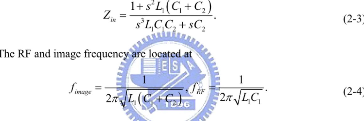
The third-order passive notch filter noted in Fig. 2.2 is introduced in [2]. The input impedance of IR filter Zin is derived as
(
)
2 1 1 2 3 1 1 2 2 1 . + + = + in s L C C Z s L C C sC (2-3)The RF and image frequency are located at
(
)
1 1 1 1 2 1 1 , . 2 2π π = = + image RF f f L C L C C (2-4)The IR filter can provides low impedance and high impedance at image frequency and RF frequency, respectively. Thus the gain will not degrade due to the parasitic capacitance. However the quality factor Q of the on-chip inductor is comparatively low, so that the peak is not sufficient deep.
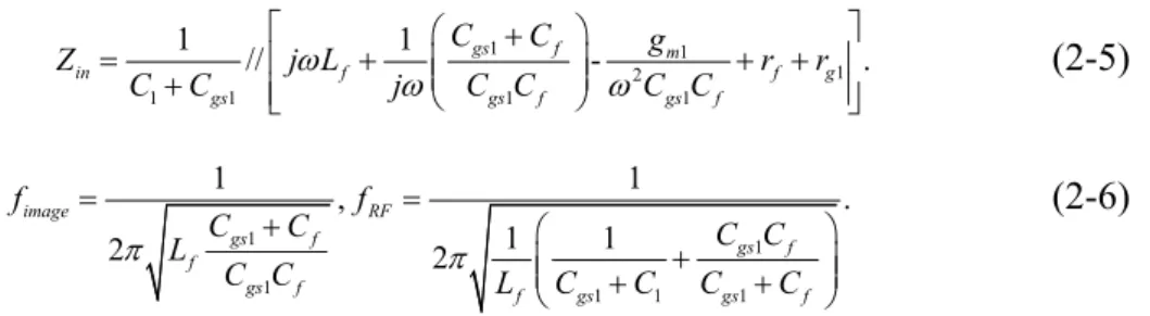
In Fig. 2.3, the improved approach of previous researches is described as followed [3]. It exploits the third-order active notch filter implemented in the signal path of cascode LNA circuit. The input impedance of the IR filter, RF frequency, and image frequency can be expressed as
1 1 1 2 1 1 1 1 1 1 // ω - . ω ω ⎡ ⎛ + ⎞ ⎤ = ⎢ + ⎜⎜ ⎟⎟ + + ⎥ + ⎢⎣ ⎝ ⎠ ⎥⎦ gs f m in f f g gs gs f gs f C C g Z j L r r C C j C C C C (2-5) 1 1 1 1 1 1 1 1 , . 1 1 2π 2π = = + ⎛ ⎞ + ⎟ ⎜⎜ + + ⎟ ⎝ ⎠ image RF gs f gs f f gs f f gs gs f f f C C C C L C C L C C C C (2-6)
where Cgs1 is the gate-to-source parasitic capacitance, gm1 is transconductance,
rg1 is the gate parasitic resistance, and rf is the parasitic resistance of the inductor.
Because Zin has negative resistance, the quality factor is unaffected by relatively low
quality factor of the on-chip inductor. At image frequency fimage, Zin is reduced to zero,
whereas at RF frequency, Zin is maximized. The loss of RF signal can be avoid.
However, the active filter will contribute extra power and noise. In addition, stack of three stages transistors in this design needs higher supply voltage (3V).
Another research like Fig. 2.4 presents the LNA with the 4th-order T structure filter in [4] and Fig. 2.5 shows the LNA with the active filter in [5]. In Fig. 2.4, the current transfer function of the T structure filter and the image frequency can be express as 4 2 1 2 1 1 2 1 2 4 2 1 1 2 2 2 1 1 2 1 2 1 1 1 . 1 1 1 1 out RF s s C C L L L C C i i s s L C L C L C L L C C ⎞ ⎛ + ⎜ ⎟ + + ⎝ ⎠ = ⎞ ⎛ + ⎜ + + ⎟+ ⎝ ⎠ (2-7) 4 1 2 1 2 1 . 2 image f L L C C π = (2-8) The current transfer function has the zero frequency at fimage, which filters out
image signal because iRF can’t pass the filter to M2 stage. But it still have no technique
to increase quality factor and the RF signal will be degraded by the T-structure filter. All approaches of above discussed researches implement IR filter into the inter-stage of a cascode LNA.
Fig. 2.5. The IR LNA with active filter.
This work presents a new design which improves current-reused technique by adding a LC tank in inter-stage to achieve simultaneously IR function and lower power dissipation than [3-5].
2.3 Conventional current-reused amplifier
Fig. 2.6 illustrates an amplifier topology called current-reused. The bias circuits of two NMOS transistors are not shown in the diagram. In this circuit, the source of upper transistor is bypassed to ground, thus both transistors operate as common-source stage, while they share the same bias current. The signal amplified by lower transistor is coupled to the gate of upper transistor by inter-stage capacitor. Two inductors as two loads of transistors have high impedance at RF frequency, so that the signal can be amplified twice. The usage of inductor instead of resistor is because the DC current leads to no voltage drop, the supply voltage can be reduced. This circuit can save power through the reuse of the bias current and obtain high gain performance.
Fig. 2.6. Conventional current-reused amplifier.
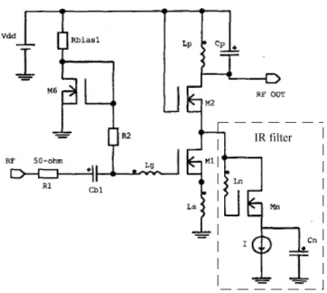
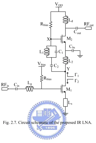
2.4 Architecture
The schematic diagram of the proposed LNA is shown in Fig. 2.7. Cbs is bypass
capacitor like short in AC. The circuit uses supply voltage (VDD) of 1V and bias
voltage (Vbias) of 0.7V. Gate bias resistor, Rbias, is large value (21 kΩ) to isolate
voltage sources from RF signal path and block noise from voltage source. Ls and Lg
are for input matching. Cin is DC blocking capacitor. The inter-stage is composed of
L1, L2, C1, and C2. Ld and Cout are for output matching. Supply voltage VDD connects a
bypass capacitor (10pF) to ground, which ensure VDD working like ground in AC. The
circuit topology uses current-reused technique, that M1 and M2 transistors are stack
like common source and use the same bias current, therefore, the total power consumption is minimized.
Fig. 2.7. Circuit schematic of the proposed IR LNA.
2.5 Design
considerations
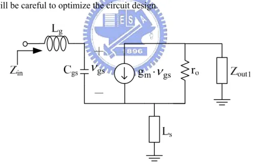
2.5.1 Input matching analysis
The proposed LNA is used to match to 50Ω, its small signal equivalent circuit of input stage is shown in Fig. 2.8, where Ls is effective inductance of M1 source to
ground; Cgs is the gate-to-source parasitic capacitance and the gate-to-drain parasitic
capacitance is ignored to simplify the process; ro is the channel length modulation
resistor of M1. Zout1 is output impedance of M1. To achieve input impedance matching,
only small Ls value is required. This Ls value is done by layout a small transmission
that area and cost can be saved. Note that Ls value is designed and optimized by an
electromagnetic simulation tool. The input impedance can be derive as
1 1 1 1 1 . ⎛ + ⎞ ⎛ ⎞ = ⎜ ⎟+ + + ⎜ ⎟ + + + + ⎝ ⎠ ⎝ ⎠ o out m s o in s g o out s gs gs o s out r Z g L r Z sL sL r Z sL sC C r sL Z (2-9) To obtain more insight on the impact of ro. we may assume
1( )= 1( ). out out
Z w jX w (2-10) For wLs <<Xout1( )w , the equation (2-1) becomes
(
)
1 1 1 . ⎛ ⎞ = + + + ⎜ ⎟ + ⎝ ⎠ m s o in s g gs gs o out g L r Z s L L sC C r Z (2-11)In this design Zout1 will be large enough at its resonance to cause a dip in the
real part of Zin and shift the resonant frequency. Therefore, the choices of device
values will be careful to optimize the circuit design.
gs
ν
m gs
g
⋅
ν
Fig. 2.8. The small signal equivalent circuit of input stage of the proposed LNA.
2.5.2 Image-rejection filter analysis
The IR filter is shown in Fig. 2.9, where Cin2 is gate parasitic capacitance of M2.
The LC tank, including L1 and C1, provides the highest dip of impedance at resonating
Fig. 2.9. Schematic of the IR filter. The voltage ratio of node X to node Y can be derived as
2 1 2 2 1 1 . 1 1 1 // = ⎛ ⎞ + + ⎜ ⎟ ⎝ ⎠ in v in sC A sL sC sC sC (2-12)
For Cin2<<C2 (Cin2≅7 , 158 fF C2 = fF ), the first tern in denominator is negligible.
Equation (2-4) can be re-written as
2 2 1 1 2 1 2 2 1 1 1 1 1 1 . 1 1 1 // 1 + ≅ = ⎛ ⎞ + + ⎜ ⎟ ⎛ ⎞ ⎝ ⎠ ⎜ + ⎟ ⎝ ⎠ in v in in s sC L C A s sL C sC sC L C C (2-13)
From equation (2-5), the image and RF signals can be located at
1 1 1 . 2π = image f L C (2-14) 2 1 1 1 1 . 2π 1 = ⎛ ⎞ + ⎜ ⎟ ⎝ ⎠ RF in f C L C C (2-15)
We can observe that Cin2 is small value contrast to C1, so that fimage can be set
close to fRF. For fimage > fRF, the image frequency must be designed slightly higher
than RF frequency.
the small signal equivalent circuit looking into the gate of M2. Transistor M2 not only
plays an amplified role, but also be exploited to achieve sufficient quality factor. The analysis ignored L2 due to its high impedance at high frequency.
gs2
ν
m2 gs2
g
⋅
ν
Fig. 2.10. The small signal equivalent circuit looking into the gate of M2.
Where Cgs2 is the gate-to-source parasitic capacitance, and rg2 is the series gate
parasitic resistance. The input impedance can be derived as
2 2 2 2 2 1 1 1 - ( ). ω ω = m + + in g gs bs gs bs g Z r C C j C C (10) Because the quality factor usually is dominated by resistance of the filter, we only discuss the real part. In (10) the second term on the right-hand side is negative resistance proportional to gm2, by adjusting M2 size, sufficient negative resistance can
be generated to cancel out rg2 and parasitic resistance of on-chip inductor L1.
Therefore, the quality factor of the IR filter will be increased to high value. Note that the analysis of input impedance has to include L2 at low frequency.
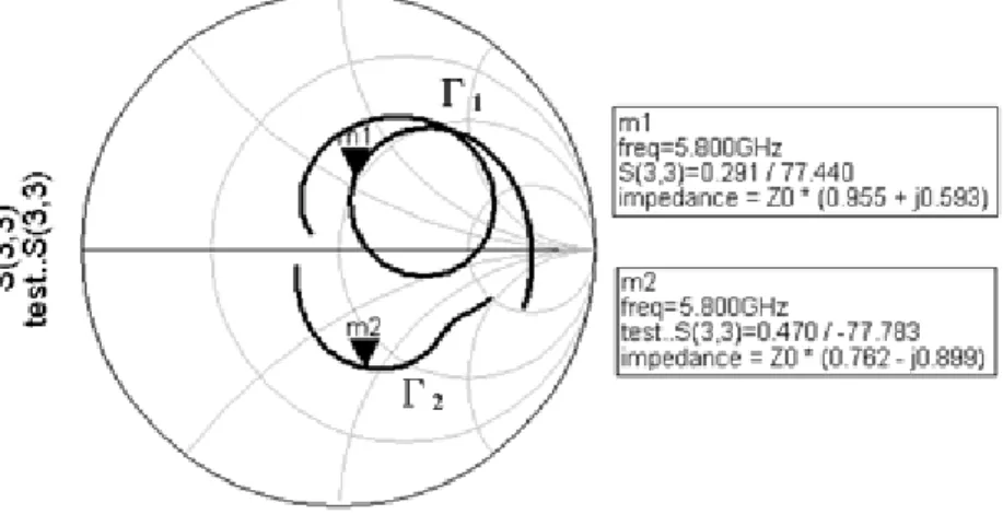
To verify IR ability of the filter, the simulation result of Av is shown in Fig. 2.11.
The RF signal at 5.8 GHz passes through the filter and image signal at 6.9 GHz is filtered out. The passive IR filter, which only requires simple circuit and exploits parasitic capacitance of M2, is implemented at inter-stage and consumes no additional
frequency and low frequency, but the simulated result is not coincident. It is because the parasitic resistances within the transmission line, the signal will be lost from node Y to node X.
In addition, the filter is also used as the inter-stage matching. Fig. 2.12 shows that at node Y, the simulated reflection coefficients Γ1 and Γ2 are approximately
complex conjugate matching from simulation result to achieve maximum power transformation. 1 2 3 4 5 6 7 8 9 10 Frequency (GHz) -30 -25 -20 -15 -10 -5 0 5 Av ( d B)
Fig. 2.11. Simulation result of Av =X Y/ in Fig. 2.7.
2.6 Chip implementation and measured results
2.6.1 Measurement considerations
The proposed LNA for WLAN has been designed based on TSMC 0.18µm mixed-signal/RF CMOS 1P6M technology and for on-wafer measurement by Chip Implementation Center (CIC). The layout follows CIC’s probe station testing rules. This circuit requires two 3-pin DC probes on upper and lower side and two RF GSG probes for RF signal on left and right side as shown in Fig. 2.13.
RFin RFout
DC DC
Fig. 2.13. On-wafer measurement of proposed IR LNA
The layout and chip photo of proposed LNA are shown in Fig. 2.14 and Fig. 2.15, respectively. The chip size is 0.75 mm × 0.93 mm including the probing pads.
Fig. 2.14. Layout of the proposed LNA.
Fig. 2.15. Micrograph of the proposed LNA.
The measurement setups for each parameter are shown in Fig. 2.16(a-d). We needs measured instruments including network analyzer, noise analyzer, spectrum analyzer, two signal generators, and two dc power supplies in CIC radio-frequency measurement environment.
(a)
(b)
(d)
Fig. 2.16. Measurement setups for (a) S-parameter. (b) noise figure. (c) P1dB. (d) IIP3.
2.6.2 Measured Results and discussion
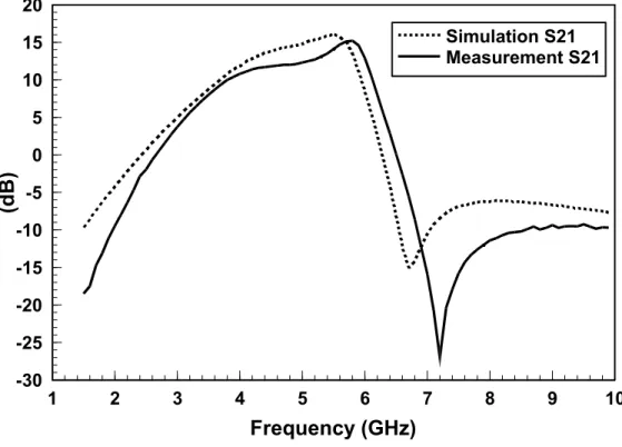
The circuit operates at supply voltage of 1 V, and consumes 6.1mW power. The S-parameter is shown in Fig. 2.17-2.20. The measured results shows that the proposed LNA at 5.9 GHz exhibits 15.2 dB power gain (S21), better than -15 dB input and
output return loss, better than -30 isolation, and -27 IR at 7.3 GHz. The simulated and measured operation frequency are at 5.8 GHz and 5.9 GHz, respectively, thus the operation frequency shifts 0.1 GHz. In addition, image frequency shifts 0.5 GHz from simulated 6.8 GHz to measured 7.3 GHz. This phenomenon is probably because the process variation and the simulated models of inductors are inaccurate. From (2-14) and (2-15), L1 determining the location of fRF and fimage, is comparatively large size so
as to easily be influenced by variation, thus L1 is the most important component and
of measured output return loss is the same as simulated. The output impedance matching is determined by Ld, which is comparatively small to defy variation. Fig.
2.21 shows the simulated and measured noise figure (NF), which both are similar before 5.9 GHz. After 5.9 GHz, simulated and measured NF are different and have the highest peaks located at each image frequency. The measured NF is 3.2 dB at 5.9 GHz. The linearity including input-referred third-order intercept point (IIP3) and input 1 dB compression point (P1dB) are shown in Fig. 2.22-2.24. It shows the measured P1dB of -19.5 dBm and the measured IIP3 of -9.5 dBm similar to the simulated results. The performance summary of the proposed IR LNA is listed in table 2.1.
1 2 3 4 5 6 7 8 9 10 Frequency (GHz) -30 -25 -20 -15 -10 -5 0 5 10 15 20 (d B ) Simulation S21 Measurement S21
Fig. 2.17. Measured and simulated gain (S21).
1 2 3 4 5 6 7 8 9 10 Frequency (GHz) -30 -25 -20 -15 -10 -5 0 (d B ) Simulation S11 Measurement S11
Fig. 2.19. Measured and simulated output return loss (S22). 1 2 3 4 5 6 7 8 9 10 Frequency (GHz) -70 -65 -60 -55 -50 -45 -40 -35 -30 -25 (d B ) Simulation S12 Measurement S12
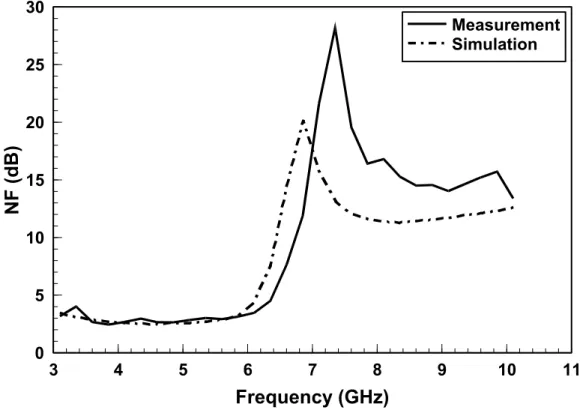
3 4 5 6 7 8 9 10 11 Frequency (GHz) 0 5 10 15 20 25 30 N F ( d B ) Measurement Simulation
Fig. 2.21. Measured and simulated noise figure (NF).
-50 -45 -40 -35 -30 -25 -20 -15 -10
RF Input Power (dBm)
9 10 11 12 13 14 15 16G
ai
n
(
d
B
)
Simulation Measurement-40 -35 -30 -25 -20 -15 -10 -5 0 Input Power (dBm) -90 -80 -70 -60 -50 -40 -30 -20 -10 0 O u tp u t P o w er ( d B m )
Fig. 2.23. Simulated IIP3.
-40 -35 -30 -25 -20 -15 -10 -5 0 Input Power (dBm) -70 -60 -50 -40 -30 -20 -10 0 O u tp u t P o w er ( d B m )
Table 2.1
Performance summary of the proposed IR LNA
Specification Measurement Post Simulation
Operation Frequency
(GHz) 5.9 5.8
Image Frequency 7.3 6.8
Input Return Loss (dB) -16.4 -16.5
Output Return Loss (dB) -15 -27
Gain (dB) 15.2 15.1 Image Rejection (dB) -27 -15 Isolation (dB) -30.3 -35.7 P1dB (dBm) -19.5 -18.9 IIP3 (dBm) -9.5 -9.4 Noise Figure (dB) 3.2 3.1 Vdd (V) 1 V 1 V
Total LNA Power (mW) 6.1 5.9
2.6.3 Comparison with other literatures
The performances of the proposed IR LNA are listed and compared with other works shown in Table 2.2. It reveals that this work has the lowest power comsumption and supply voltage due to the current-reused configuration. The proposed LNA also has good IR capability compared with [3]. Although [4] and [5] shows the better performance of IR, it is only simulated results. It is difficult to filter
out the unwanted signal with a deep peak due to the low quality factor Q of the on-chip component. The performances of the proposed LNA satisfy the system specification and chip size is comparatively small.
Table 2.2
Comparison of the IR LNA performances S11 (dB) S22 (dB) Gain (dB) IR (dB) NF (dB) IIP3 (dBm) VDD (V) Power (mW) This work (meas.) -16.4 -15 15.2 -27 3.2 -9.5 1 6.1 [3] (meas.) -18 -20 20.5 -20 1.5 -5 3 12 [4] (sim.) N/A N/A 11 -35 3 -10 1.5 6.3 [5] (sim.) -21 N/A 10 -65 2.4 -10 1.5 10.3
Chapter 3
Design of Current-Reused LNA for UWB
3.1 Introduction
The requirement for high-speed wireless communication systems has increased significantly during the last few years. The FCC has allocated 7500-MHz bandwidth in the 3.1–10.6 GHz frequency range (low-frequency band: 3.1–5 GHz; 4high-frequency band: 6–10.6 GHz) for UWB application. The UWB technology, including the IEEE 802.15 standard, is considered as an attracted wireless interface because of its potential to provide high data rate, low power consumption, and low cost. The UWB communication is allowed very low average transmit power compared with more conventional systems for short range and high rate connectivity, that can be applied to Wireless Personal Area Network (WPAN).
The design of the front-end LNA is one of the challenges in the RF receivers. LNA’s purpose is to amplify the received signal from the antenna with as weak signal and additional noise as possible. Because it is a first building block in the RF receiver, its performance dominates the sensitivity of the overall system. Hence, for the achievement of high receiver sensitivity, the LNA is required to have a low noise figure with good matching network between the antenna and the LNA as well as sufficient gain with flatness in the wide frequency range of operation.
3.2 Numerous topology of wideband LNA
The amplifiers that can provide 50 Ω input impedance over a wide bandwidth are the challenge. Some researches about wideband amplifier will be discussed as follow.
Fig. 3.1 shows resistor-terminated common-source amplifier, common-gate amplifier, and resistive shunt-feedback amplifier .
Fig. 3.1. Conventional wideband configurations. (a) Resistor-terminated common-source amplifier. (b) Common-gate amplifier. (c) Resistive shunt-feedback amplifier.
The three configurations of amplifiers all can achieve 50 Ω wideband input matching, however, they have some drawbacks. In Fig. 3.1(a), The Resistor-terminated common-source amplifier achieves wideband matching by setting RT equal to 50 Ω, but it loses a lot of voltage due to the loading effect, the voltage
gain will decrease. In Fig. 3.1(b), the CG amplifier has small input resistance of 1/gm
to achieve wideband input matching, however it is noisier than common-source amplifier. The noise figure can be improved by increasing gm, but the input matching
will be difficult to obtain over wide bandwidth. In Fig. 3.1(c), an alternate approach for wideband amplifier is the resistive shunt-feedback amplifier. It exploits negative feedback method to get lower input impedance, more stability, but lower voltage gain, so that noise of next stages won’t be suppressed due to gain degradation.
Fig. 3.2 shows the distributed amplifier that can provide wide band matching by several stages, and relatively flat gain over 3.1-10.6 GHz UWB band can be achieve in recent research [6]. However, the drawback is large power consumption due to multiple transistors stages, and the usage of much inductors occupies large die area, which make them unsuitable for integration. In addition, the research shows the distributed amplifier cannot achieve sufficient gain compared with other configurations.
Fig. 3.2. Conventional distributed amplifier.
In recent research, a wideband input matching approach has been presented. Fig. 3.3 is the simple small signal equivalent circuit of common-source amplifier with inductive source degeneration, and load resistance and capacitance at the drain of transistor are shown in the diagram. The input impedance depends on resistive load and capacitive load at high frequency and low frequency, respectively. The wideband impedance matching and noise matching can be achieved without extra matching network [7].
Fig. 3.3. The small signal equivalent circuit of CS amplifier with inductive source degeneration.
Here, this work is designed based on resistive shunt-feedback amplifier. To improve gain performance, the current-reused technique will be adopted to enhance gm. The traditional current-reused amplifier [8] is expressed in Fig. 3.4.
V
inV
outFig. 3.4. Current-reused amplifier.
3.3 Architecture
The proposed UWB LNA employs three stages as shown in Fig. 3.5. This circuit is designed to require two bias voltage sources of 1.5 V (Vdd) and 0.7 V (Vbias).The
first input stage including M1n and M1p is current-reused configuration. It can achieve
common-source which be used to enhance the gain. The output stage M3 is also
common-source configuration. But its main object is to make output impedance match 50 Ω for measurement purpose. Each inter-stage places an on-chip bypass capacitor (3 pF) to avoid DC bias current flowing into the front stage. A large resistor (17 kΩ) is employed in each bias circuit to isolate noise of voltage source from internal circuit. The function of Cg (1 pF) in input stage is to make the gate voltages of M1p and M1n
can be set different. M1n always operates at saturation region due to Rf feedback,
whereas M1p can change its gate voltage due to Cg for fine tuning.
Fig. 3.5. Schematic of the proposed UWB LNA.
3.4 Design
considerations
For resistive shunt-feedback amplifier in Fig. 3.1(c), because the transfer function has a dominant pole by Miller effect, the -3 dB bandwidth can be given by
(
)
(
)
-3 1 | | . 1 | | V dB F gs gd V A R C C A ω = + + + (3-1)where AV is open-loop gain and Cgs and Cgd are the intrinsic capacitance of the
transistor. From (3-1), wider bandwidth can be obtained by higher |AV| and smaller RF.
However, small RF leads to degradation of noise figure and gain. The better approach
to enlarge bandwidth is increase of |AV|. For this purpose, this work improves resistive
shunt-feedback amplifier to current-reused amplifier for enhancement of transconductance to obtain higher gain. The analysis of current-reused amplifier is similar to resistive shunt-feedback amplifier.
3.4.1 Gain analysis
By stacking NMOS M1n and PMOS M1p transistors, the RF signal will be
amplified by two common-source amplifiers, which share the same bias current so as to lower the power consumption. In other words, the transconductance of input stage will be increased from gm to approximately 2gm. In addition, Rf is designed large
value (6 kΩ) to avoid gain degradation.
3.4.2 Input matching analysis
The proposed LNA is designed to match to 50 Ω, the input small signal equivalent circuit is shown in Fig. 3.6, where Zo is output impedance of
current-reused stage; ro is shunt channel length modulation resistor of both M1n and
M1p;Ls =Ls1// Ls2; gm =gmn+gmp. For simplicity, parasitic capacitances of input
stage transistors are neglected. Because Cg is DC block capacitor, it can also be
Fig. 3.6. The small signal equivalent circuit of input stage.
At first, we assume Ls =0, 0,Lg = the input impedance Zin can be easily
expressed as
(
)
1
.
+
=
+
&
&
f o o in m o oR
Z
r
Z
g
Z
r
(3-2)We can observe that the input impedance of resistive shunt-feedback amplifier is equal to (3-2), except for enhancement of gm in this design. By (3-2),
the common-source amplifier can reduce input resistance by Rf feedback because
of the Miller effect so as to achieve 50 Ω impedance matching. Note that Rf must
be enough large value to maintain gate-to-drain isolation and minimize the noise. If we consider parasitic capacitance of input stage, the input return loss will be degraded at higher frequency due to the large input parasitic capacitance by Miller effect. The current-reused configuration by stacking NMOS and PMOS increases not only transconductance by gm=gmn+gmp, but also parasitic capacitance by
Cgs=Cgsn+Cgsp and Cgd=Cgsn+Cgsp. The effective input capacitance will be
amplified more seriously. For this purpose, Ls and Lg are added for better input
matching at high frequency. Here, the input impedance Zin including Ls and Lg can
(
)
(
)
1 - 1 1 1 1 - 1 1.
+ + + + + = + + + + + + +⎛
⎞
⎜
⎟
⎛
⎞
⎜
⎟
⎜
⎟
⎜
⎟
⎝
⎠
⎜
⎟
⎝
⎠
⎛
⎞
⎜
⎟
⎜
⎟
⎜
⎟
⎜
⎟
⎝
⎠
f o o f m o o o m o s in g o m o m o m o o o m o s R r r R g r r Z g r sL Z sL r g r g r g r r Z g r sL (3-3)The simulated results of input and output reflection coefficients are shown in Fig. 3.7 and Fig. 3.8. We can observe that the curve is around the center of the Smith chart over UWB band from 3.1GHz to 10.6GHz. It shows that this design and analysis can successfully achieve wideband input impedance matching.
Fig. 3.8. Simulated result of output reflection coefficient
3.5 Chip implementation and measured results
3.5.1 Layout considerations
The layout is very important for radio-frequency integrated circuit, because high frequency will make more parasitic and coupling effects occur to influence performances. All pads and important path line use bottom ground metal and guard-rings are added with all components for shielding to prevent noise and interference from substrate. The RF pad size is 50 x 50 um2, which is the smallest accepted size according to CIC testing rule. Because the bottom ground metal is used as shielding, the RF pad has parasitic capacitance which will degrade the RF signal. Thus the smaller pad can lead to a smaller parasitic capacitance. In this design, the pas size of 50 x 50 um2 has capacitance value approximately equal to 22fF, which be contained in simulation. All interconnections between elements are taken as a 45° corner. The bypass capacitors are added between each voltage source node and ground node to ensure voltage source working like ground in AC and filter out noise.
A DC-blocking capacitor is needed in the input of the UWB LNA circuit to isolate DC current between the circuit and instrument. All transmission lines of signal path are simulated by an electromagnetic software to find out the parasitic and coupling effects in order to make the simulated results more accurate.
3.5.2 Measurement considerations
The layout of the proposed LNA is shown in Fig. 3.9. The chip layout must be according to CIC’s probe station testing rules for on-wafer measurement. This circuit requires two RF GSG probes placed on opposite sides of the layout for RF signal input and output, a 3-pin DC probe, and a 6-pin DC probe. The fabricated chip photo with testing probes is shown in Fig. 3.10. All probes are pitch 100 µm for saving area. Fig. 3.11 expresses the arrangement of RF and DC probes.
Fig. 3.10. Microphotograph of the UWB LNA with probes.
RF
inRF
outDC
DC
The chip is measured in CIC RFIC testing environment. The measurement equipments include a network analyzer, a noise analyzer, a spectrum analyzer, two signal generators, and several dc power supplies. The measurement setup for S-parameters, noise figure, input 1dB compression point and input-referred third-order intercept point are shown in Fig. 3.12(a-d).
Network
Analyzer
(a)
(c) Signal Generator 1 Spectrum Analyzer Signal Generator 2 Combiner (d)
Fig. 3.12. Measurement setups for (a) S-parameter. (b) noise figure. (c) P1dB. (d) IIP3.
3.5.3 Measured and simulated results
The proposed LNA for UWB system has been fabricated on TSMC 0.18 µm mixed-signal/RF CMOS 1P6M technology with chip size of 0.949 x 0.912 mm2. The total power consumption is 14.4 mW with bias voltage source 1.5 V and 0.7 V. The S-parameter are shown in Fig. 3.13-3.16. The input return loss (S11) in Fig. 3.13 shows the measured S11 lower than -10 dB, which degrades about maximum 2 dB compared with simulated result at 7 GHz. Fig. 3.14 indicates the measured and simulated output return loss (S22). The measured S22 is lower than -17 dB and the experimental result reveals measured S22 is better than simulated S22. The gain (S21) is an important parameter of a LNA. The measured S21 degrades about 2 dB and 1 dB at low frequency and high frequency than simulated S21, respectively. The measured S21 in 3.1-10.6 frequency band is 11.9 dB to 16.4 dB, which is not flat in UWB band. The noise figure (NF) performance is shown in Fig. 3.17. The measured NF has maximum 5.28 dB and minimum 3.33 dB, which is higher than simulated NF perhaps due to the inaccurate noise model and post-simulation. The input-referred 1dB compression point (P1dB) are shown in Fig. 3.18(a-e). The measured P1dB are -18.3 dBm at 3.1 GHz, -18.5 dBm at 4.9 GHz, -18.5 dBm at 6.8 GHz, -15.6 dBm at 8.7 GHz, and -11.7 dBm at 10.6 GHz. The input-referred third-order intercept point (IIP3) at five frequency points are shown in Fig. 3.19(a-e). The measured IIP3 shows -8.2 dBm at 3.1GHz, -9.5 dBm at 4.9 GHz, -9 Bm at 6.8 GHz, -2.6 dBm at 8.7 GHz, and 0 dBm at 10.6 GHz. The performance summary is listed in table 3.1.
2 3 4 5 6 7 8 9 10 11 12 Frequency (GHz) -25 -23 -21 -19 -17 -15 -13 -11 S 11 ( d B ) Measurement Simulation
Fig. 3.13. Measured and simulated results of S11.
2 3 4 5 6 7 8 9 10 11 12 Frequency (GHz) -60 -55 -50 -45 -40 -35 -30 -25 -20 -15 -10 -5 S 2 2 (d B ) Measurement Simulation
2 3 4 5 6 7 8 9 10 11 12 Frequency (GHz) 4 6 8 10 12 14 16 18 20 S 21 (d B ) Measurement Simulation
Fig. 3.15. Measured and simulated results of S21.
2 4 6 8 10 12 Frequency (GHz) -100 -90 -80 -70 -60 -50 -40 -30 S 12 ( d B ) Measurement Simulation
2 3 4 5 6 7 8 9 10 11 12
Frequency (GHz)
2 3 4 5 6 7N
F
(
d
B
)
Measurement Simulation-30 -25 -20 -15 -10 INPUT_POWER (dBm) 5 6 7 8 9 10 11 12 13 14 15 O U T P U T _P O W E R ( d B m ) Measurement @ 3.1GHz Simulation @ 3.1GHz (a) -30 -25 -20 -15 -10 INPUT_POWER (dBm) 8 9 10 11 12 13 14 15 16 17 O U T P U T _P O W E R ( d B m ) Measurement @ 4.9GHz Simulation @ 4.9GHz (b) -30 -25 -20 -15 -10 INPUT_POWER (dBm) 8 9 10 11 12 13 14 15 16 17 OU T P U T _P OW E R ( d B m ) Measurement @ 6.8GHz Simulation @ 6.8GHz (c)
-30 -25 -20 -15 -10 INPUT_POWER (dBm) 9 10 11 12 13 14 15 16 O U T P U T _ P O W E R ( d B m ) Measurement @ 8.7GHz Simulation @ 8.7GHz (d) -30 -25 -20 -15 -10 -5 INPUT_POWER (dBm) 5 6 7 8 9 10 11 12 13 14 O UT P UT _P O W E R (d B m ) Measurement @ 10.6GHz Simulation @ 10.6GHz (e)
Fig. 3.18. Measured and simulated results of P1dB at (a) 3.1 GHz. (b) 4.9 GHz. (c) 6.8GHz. (d) 8.7 GHz. (e) 10.6 GHz.
-40 -35 -30 -25 -20 -15 -10 -5 INPUT_POWER (dBm) -80 -70 -60 -50 -40 -30 -20 -10 0 O U T P U T _ P O W E R ( d B m) Measured IIP3 @ 3.1GHz (a) -40 -35 -30 -25 -20 -15 -10 -5 INPUT_POWER (dBm) -80 -70 -60 -50 -40 -30 -20 -10 0 O U T P U T _P O W E R ( d B m) Measured IIP3 @ 4.9GHz (b) -40 -35 -30 -25 -20 -15 -10 -5 INPUT_POWER (dBm) -80 -70 -60 -50 -40 -30 -20 -10 0 O U T P U T _P O W E R ( d B m) Measured IIP3 @ 6.8GHz (c)
-40 -35 -30 -25 -20 -15 -10 -5 0 INPUT_POWER (dBm) -90 -80 -70 -60 -50 -40 -30 -20 -10 0 O U T P U T _ P O W E R ( d B m ) Measured IIP3 @ 8.7GHz (d) -40 -35 -30 -25 -20 -15 -10 -5 0 INPUT_POWER (dBm) -90 -80 -70 -60 -50 -40 -30 -20 -10 0 O U T P U T _ P OW E R ( d B m ) Measured IIP3 @ 10.6GHz (e)
Fig. 3.19. Measured result of IIP3 at (a) 3.1 GHz. (b) 4.9 GHz. (c) 6.8GHz. (d) 8.7 GHz. (e) 10.6 GHz.
Table 3.1
Performance summary of the proposed LNA
Specification Measurement Post Simulation
Input Return Loss (dB) -16.8~-10.6 -19.8~-14.1
Output Return Loss (dB) -58~-16.7 -21.4~-13.6
Gain (dB) 14.1± 2.3 14.75 ± 1.85 Isolation (dB) -64.6~-40 -73.8~-36.8 P1dB (dBm) -18.7~-11.7 -20.2~-13.7 IIP3 (dBm) -9.5~0 -12.5~-3.5 Noise Figure (dB) 3.3~5.3 2.7~3.8 Vdd (V) 1.5 V 1.5 V
Total LNA Power (mW) 14.4 11.6
3.5.4 Comparison with other literatures
The performances of the proposed UWB LNA are compared with other works for UWB band listed in Table 3.2. This work has the smallest ratio of average gain to power approximately equal to 1. It reveals that the current-reused configuration can efficiently enhance the gain performance. In 3.1-10.6 GHz, the proposed LNA exhibits average gain of 14.1 dB while consumes 14.4 mW power. The NF of the proposed LNA also has better performance at lower frequency than other works based on CMOS 0.18 um process. In addition, no buffer is required in this design, however, table 3.2 shows that this work has the best output return loss, which is lower than -16.7 dB over UWB band.
Table 3.2
Comparison of Ultra Wide-band LNA
Ref. Process BW (GHz) S11 (dB) S22 (dB) Gain ave.(dB) NF (dB) IIP3 Power (mW) This work (Meas.) 0.18um CMOS 3.1~10.6 <-10.6 <-16.7 14.1 3.3~5.3 -9.5~0 14.4 [9] 2005 (Meas.) 0.18um CMOS 3.1~10.6 <-11 <-14 8.85 4.5~5.1 -6.2* 20 [10] 2004 (Sim.) 0.18um CMOS 3.1~10.6 <-10 <-9 18 5~7 N/A 54 [11] 2007 (Meas.) 0.18um CMOS 3.1~10.6 <-9.7 <-8.4 11.4 4.12~5.16 0.72# 22.7 [12] 2008 (Meas.) 0.13um CMOS 3.1~10.6 <-17.5 <-14.4 7.92 2.5~4.56 -4* 10.68 [13] 2006 (Meas.) 0.13um CMOS 3.1~10.6 <-9.5 N/A 9.4 3.6~4.95 -7.2* 19
*At 6 GHz, #At 6.4 GHz
Chapter 4
Design of Low-Power High-Linearity
Inductorless Mixer for UWB
4.1 Introduction
RF CMOS technology is developed to achieve higher frequency and wider bandwidth application. Large-scale availability of CMOS allows devices to be manufactured at a much lower cost as compared with devices that depend on non-silicon technologies. The UWB communication system over 3.1 GHz to 10.6 GHz frequency band will be widely used in the short distance WPAN, providing high data rates to a large number of users over large area.
In the chain of down-conversion UWB receiver, the mixer plays a key role to shift RF signal to IF. The researches of wideband matching for the mixer have developed. For example, the matching network for the mixer can employ distributed network [14] and LC ladder network [15] as shown in Fig. 4.1 and Fig. 4.2, respectively. However, both methods require inductors that occupy large die area that is unsuitable for integration.
Fig. 4.1 The mixer using the distributed matching network.
Fig. 4.2. The mixer using the LC ladder matching network.
High linearity receiver is essential for high data rate communication system. The second stage should consider the linearity performance because the last stage is a prominent contributor to degrade the linearity. For a cascaded amplifier, the total input-referred third-order intercept point (IIP3total) can be expressed as
2 2 2
1 2 3
1 1
.
3total 3 3 3
IIP IIP IIP IIP
α α β
≅ + + +" (4-1) where α and β are the linear gain for the first and second stages, respectively. From
(4-1), we can observe that the IIP3 of the last stage significantly affects the total IIP3. In addition, because LNA usually designed for high gain to suppress the noise of next stage, it is difficult to maintain comparatively better linearity. In general, the linearity of the receiver is dominated by a mixer. The linearity performance requirement becomes more significant in modern RF mixer for improvement of the receiver dynamic range and immunity to the various interferer signals from other communication standards.
In this work, a low-power, high-linearity wideband down-conversion mixer without the use of inductors is designed and implemented using TSMC 0.18 µm CMOS process. The circuit will be analyzed and discussed.
4.2 Architecture
In Fig. 4.3, the proposed mixer is based on Gilbert-cell topology, which is double balance mixer to suppress LO-to-IF feed though compared to single balance mixer. Three voltage sources (VDD=1.8 V, VB=0.77 V, VS=0.63 V) are used in the circuit. The
bias voltage, VB, at switching stage is not shown in the diagram. The transistors of
switching stage with small W/L are sufficiently fast to steer the RF current from transconductance stage to switching stage. The gate-to-source voltage (Vgs) is set near
threshold voltage (Vt) for completely current commutation. The differential output
employs the buffer to provide 50 Ω output impedance for on-wafer measured requirement. In this work, some techniques will be exploited to improve linearity of the mixer.
Fig. 4.3. Schematic of the proposed mixer.
4.3 Design
considerations
4.3.1 Common-gate transconductance stage with
source resistor
The proposed mixer employs common-gate (CG) amplifier as transconductance stage. The CG configuration adding a source resistor can improve linearity. To observe this phenomenon, we derived the voltage gain (AV) of CG amplifier as
= +In2 1. V S In R A R R (4-2) where 1≅ 1 . In m R g (4-3) and RIn2 is second stage input resistance. From (4-2), additional source resistor RS will
stabilize the voltage gain throughout operation. If the transconductance value gm
varies, the operation point will not vary as much. Therefore, CG amplifier with source resistor can maintain stability of operation point against variation in transistor parameters. However, the trade-off is that the voltage gain will degrade because of source resistor.
The CG configuration also has wide bandwidth to achieve better linearity compared to common-source (CS) configuration. The high-frequency response of CG amplifier is shown in Fig. 4.4, where CIn2 is second stage input capacitance. For
simplicity, channel length modulation is negligible because RIn2 is relatively small. In
such case, there are two poles given by
(
)
ω
1= 1 1 . // P gs In S C R R (4-4)(
)
ω
=
+
2 2 21
.
P gd In InC
C
R
(4-5)The frequency response can be derived as
( )
=(
ω
)(
ω
)
+ + + 2 1 2 1 . 1 1 / 1 / m In V m S P P g R G s g R s s (4-6) Fig. 4.4. CG amplifier.Besides, in Fig. 4.5, CS amplifier also has two poles obtained as
(
) ( )
ω
= ⎡ + + ⎤ ⎣ ⎦ 1 2 1 . 1 P gs gd m In S C C g R R (4-7)(
) (
)
ω
= ⎡ + + ⎤ ⎣ ⎦ 2 2 2 2 1 . 1 1/ P In gd m In In C C g R R (4-8) If CS voltage gain is enough large, ωP1 will dominate the high-frequencyresponse due to Miller effect. Therefore, the voltage gain of CS configuration begins to decay at lower frequency. Here, although RIn2 is relatively small, which reduces the
gain, the CG bandwidth is still better than CS bandwidth.
In general, 50 Ω input matching is difficult for CS stage due to its large input resistance. For this purpose, matching network including inductors is required. However, inductors are usually large so that impedes the level of integration. In this work, CG configuration provides excellent input-matching over wide bandwidth by setting RS+1/gm ≅50 Ω, which is suitable for UWB application.