Structural and Electrical Properties of Conducting Diamond
Nanowires
Kamatchi Jothiramalingam Sankaran,
†Yen-Fu Lin,
‡Wen-Bin Jian,
‡Huang-Chin Chen,
§Kalpataru Panda,
⊥Balakrishnan Sundaravel,
⊥Chung-Li Dong,
#Nyan-Hwa Tai,*
,†and I-Nan Lin*
,§ †Department of Materials Science and Engineering, National Tsing Hua University, Hsinchu 30013, Taiwan, ROC‡Department of Electrophysics, National Chiao Tung University, Hsinchu 30010, Taiwan, ROC §Department of Physics, Tamkang University, Tamsui 251, Taiwan, ROC
⊥Materials Science Group, Indira Gandhi Centre for Atomic Research, Kalpakkam 603 102, India
#Scientific Research Division, National Synchrotron Radiation Research Center, Hsinchu 30076, Taiwan, ROC
ABSTRACT: Conducting diamond nanowires (DNWs)films have been synthesized by N2-based microwave plasma
enhanced chemical vapor deposition. The incorporation of nitrogen into DNWs films is examined by C 1s X-ray photoemission spectroscopy and morphology of DNWs is discerned using field-emission scanning electron microscopy and transmission electron microscopy (TEM). The electron diffraction pattern, the visible-Raman spectroscopy, and the near-edge X-ray absorptionfine structure spectroscopy display the coexistence of sp3 diamond and sp2 graphitic phases in
DNWsfilms. In addition, the microstructure investigation, carried out by high-resolution TEM with Fourier transformed pattern, indicates diamond grains and graphitic grain boundaries on surface of DNWs. The same result is confirmed by scanning tunneling microscopy and scanning tunneling spectroscopy (STS). Furthermore, the STS spectra of current−voltage curves discover a high tunneling current at the position near the graphitic grain boundaries. These highly conducting regimes of grain boundaries form effective electron paths and its transport mechanism is explained by the three-dimensional (3D) Mott’s variable range hopping in a wide temperature from 300 to 20 K. Interestingly, this specific feature of high conducting grain boundaries of DNWs demonstrates a high efficiency in field emission and pave a way to the next generation of high-definition flat panel displays or plasma devices.
KEYWORDS: diamond nanowire films, graphitic grain boundary, high resolution transmission electron microscopy, scanning tunneling spectroscopy, hopping transport, electron field emission
1. INTRODUCTION
Field-emission displays (FEDs) have received interest as the next-generation flat panel displays, substitute to the presently dominant liquid crystal, because of their potential low cost and high performance. One of the major concerns in FEDs has been the improvement of consistent, efficient cold cathode materials for electron field emitters.1−4 Materials like semi-conductor nanowires or nanotubes, carbon nanotubes (CNTs), and diamondfilms have been demonstrated to show low turn-on voltages and high current densities, making them suitable for cold cathode emitter applications. Among them, diamondfilms have been reported to exhibit negative electron affinity, which makes diamond a more promising material for applications in FED devices.5−8 On the other hand, one-dimensional (1D) materials showing distinct chemical and physical properties have attracted a tremendous amount of attention and have been used in many technological applications such as pH sensors,9 ultraviolet nanolasers,10 and nanoelectronics.11−13 Since the discovery of CNTs in 1991,14a variety of 1D materials were successfully synthesized.10,15 Among those 1D materials,
diamond nanowires (DNWs) were of great interest because theoretical studies and simulations explain their structural stabilities and inspire several potential applications.16−18 Especially, through their intrinsic dependence on size and crystallographic directions, DNWs were found to be energeti-cally favored and structurally stable at diameters ranging from 2.7 to 9.0 nm.16,17 Recently, novel properties including high thermal conductivity and zero strain stiffness of DNWs and related carbon materials have been theoretically predicted and experimentally demonstrated, foreseeing their feasible use in cross-link facilitated heat transfer and thermal management systems.19,20
The synthesis of DNWs is always an interesting subject since new approaches pave the way to nanoscale and atomic precision of material growth and to the search of new forms of carbon. The DNW precursor of porous diamondfilms was
Received: October 22, 2012
Accepted: January 17, 2013
Published: January 17, 2013
(EFE) properties attainable for UNCD films. Incorporation of N2 (about 20%) in Ar/CH4 plasma generated a nanowire
morphology and rendered the UNCD films a high electrical conductivity. Through microscopy and other physical in-spections, it was further argued that the notable increase in conductivity was in relation to the fact of nanowires encased by a sheath of sp2-bonded carbon.23,27−29 Additionally, the
incorporation of N2 was preferentially in the diamond grain
boundary30 that enhances the electron transport in UNCD films and demonstrates a prominent potential for an application as an electronfield emitter.26,31Nevertheless, the mechanisms of a high conductivity in DNWs and their superior EFE behavior are not well understood yet.
To solve the issue of conducting mechanism in DNWs, the temperature behavior of resistivity that unveils the electron transport in DNWs need to be explored in detail. In a previous report, temperature-dependent resistivity of N2-doped UNCD films was obtained and thermally activated conduction mechanisms with different activation energies were noticed.27 Besides, it was proposed that the enhanced conductivity exists in diamond grain boundaries. Moreover, latter studies show that Mott’s three-dimensional variable range hopping (3D VRH) theory, Efros-Shklovoskii’s hopping conduction, or other new integrated model of hopping conduction were adopted to analyze data of lightly or heavily N2-doped UNCDfilms.32−34 The heavily doped UNCD films were like a special kind of disordered metal, showing a negative magnetoresistance of weak localization35 or a logarithmic temperature-dependent conductivity of electron−electron interaction.36 However, it was theoretically argued that the negative magnetoresistance originates from strong rather than weak localization.37On the other hand, in the temperature range from 300 to 700 K the high conductivity of UNCD films can be explained by a transition from Mott’s 3D VRH to defect-band conduction transport.38 Until now, the conduction mechanism in DNWs has not been studied from both microscopically and macro-scopically electrical measurements.
In this paper, we reported the electrical mechanism of the enhanced conductivity and EFE characteristics of DNWsfilms from a microscopic viewpoint by using scanning tunneling microscope (STM) and scanning tunneling spectroscopy (STS). The conducting regimes at both grains and grain boundaries were examined in detail. Moreover, the microscopic picture of conducting mechanism can be integrated with a macroscopic (or mesoscopic) viewpoint of electron transport obtained from the temperature dependent resistivity with a careful analysis.
2. EXPERIMENTAL SECTION
2.1. Growth of DNWs Films. DNWs films with a thickness of ∼800 nm were grown on mirror polished Si (100) substrates by using
spectroscopy (Lab Raman HR800, Jobin Yvon,λ: 632.8 nm), X-ray photoemission spectroscopy (XPS; PHI 1600), secondary ion mass spectroscopy (SIMS; Cameca IMS-4f) and near-edge X-ray absorption fine structure (NEXAFS) spectroscopy. Hall measurements were carried out in a van der Pauw configuration (ECOPIA HMS-3000) to measure the electrical conductivity of thefilms.
2.3. Electrical Measurements. Conducting paths in DNWsfilms at either grains or grain boundaries were investigated elaborately by STM (150 Aarhus, SPECS GmbH) in an ultrahigh vacuum of 10−10 Torr at room temperature (RT). STM tips were prepared by electrochemical etching of tungsten wires with a diameter of 0.3 mm. STM images were taken in a constant current mode with a set current of 0.59 nA and a bias voltage of−3.75 V. Current image tunneling spectra (CITS) with voltages ramping from−5 to 5 V were measured simultaneously during the STM image scanning. A STS spectrum was calculated from an average of many CITS data.
To address electron transport mechanism of the DNWsfilms from macroscopic viewpoint, the DNWsfilms were put on a prepatterned device substrate with pairing electrodes separated by a∼200-nm wide gap for temperature dependence of electrical measurements. Si wafers capped with a 300-nm SiO2 layer were used as device substrates for
deposition of patterned, pairing Ti/Au (10/50 nm in thickness) electrodes. By etching in HF:HNO3(1:1) solution, DNWsfilms were
detached from growth substrates and formed free-standingfilms in the solution. The free-standing DNWsfilms were dispersed in acetone. A prepatterned device substrate containing pairing electrodes was then immersed into this solution and was moved up slowly such that the DNWs deposited onto the device randomly when the acetone dried. No special effort was needed to immobilize the DNWs. The DNWs films were checked to make an Ohmic contact on top of Ti/Au electrodes.39 The pairing electrodes were taken as source and drain electrodes for probing electrical properties of DNWs sitting in∼200 nm wide nanogap. The as-fabricated DNWs devices were mounted in a closed-cycle refrigerator (CRYO Industries of America Inc.) with a background pressure of 1 × 10⁻⁶ Torr for temperature dependent studies. Current−voltage (I−V) data were measured by Keithley 6430 source meter. Electrical conductance was calculated in the linear I−V regime near zero-bias voltage. Conductivities were evaluated from the conductance and the dimensions of DNWs between pairing electrodes.
On the other hand, EFE characteristics of the DNWs were measured using a molybdenum rod with a diameter of 2 mm as anode and I−V curves were acquired using Keithley 237 electrometer. The EFE behavior of materials was explained using Fowler-Nordheim (F− N) theory.40The turn-onfield was estimated from the interception of the straight lines extrapolated from the low- and high-field segments of the F−N (viz. ln(J/E2)− 1/E) plots.
3. RESULTS AND DISCUSSION
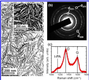
3.1. Material Characterizations. Figure 1a shows a typical low-magnification TEM image of DNWs films, revealing highly dense and uniformly distributed nanowire morphology. These randomly oriented DNWs have a length of 50−200 nm with a few nanometers in diameter. Its FESEM image which reveals the last-minute growth of surface structure is displayed in the
inset of Figure 1a. The TEM-corresponding selective area electron diffraction (SAED) pattern of the DNWs film is shown in Figure 1b, which exhibits ring-shaped patterns, implying random orientation of DNWs that are observed in the TEM image (Figure 1a). According to the SAED pattern, the lattice-plane spacings of (311), (220), and (111) are estimated to be 0.11, 0.12, and 0.21 nm, respectively, which are in line with the crystalline diamond structure. The result confirms that DNWs films are mainly constituted of diamond nanocrystals with nanowire morphology. On the other hand, there is a prominent diffusing ring in the center of the SAED pattern, signifying the existence of graphitic phase (or a-C) in DNWsfilms.
Figure 1c shows a visible-Raman spectrum having an excitation wavelength of 632.8 nm. The spectrum of DNWs shows a predomination of the sp2-bonded carbon phase
(D-band41 around 1335 cm−1 and G-band around 1590 cm−1). Additionally, a peak at 1140 cm−1is observed. It corresponds to the trans-polyacetylene (t-PA) and marks an alternate chain of sp2carbon atoms with single hydrogen bonded to each carbon
atom.42−44Notably, the characteristic diamond resonance peak at 1332 cm−1 is not clearly observable, due to the over-whelmingly high sensitivity of visible-Raman to the sp2-bonded structure over that of the sp3-bonded one. All these features in
both of the visible-Raman scattering and the TEM SAED indicate that the overall structure of DNWs is dominated by the sp2-sites in the presence of sp3-bonded carbon as well as t-PA chains.
Figure 2 shows a NEXAFS C-K edge of DNWs. Except for a typical sp2-bonded carbon characteristic peak at 285.0 eV,
NEXAFS of DNWs is very similar to that of a single crystalline diamond. It demonstrates unambiguously one specific feature of a diamond exciton sharp peak at 289.0 eV and the other specific feature of a large dip at 302.5 eV which represents a second absolute gap in the diamond band structure.28,45,46This corroborates again the coexistence of sp3 diamond and sp2
graphitic phases in DNWsfilms that is in line with the
visible-Raman and TEM results. To understand how nitrogen doping results in the chemical bonding of DNWs more precisely, XPS measurements were carried out. The C 1s photoemission spectrum of DNWs is shown in the inset of Figure 2. The data arefitted with Lorentzian functions to identify peaks at binding energies of 284.5, 285.1, 285.6, and 286.2 corresponding to CC; sp2, C−C; sp3, CN, and C−N bonds, respectively.
The background was subtracted using Shirley’s method.47The sp2CC bonding is predominant with a peak intensity of 35%
and sp3C−C intensity is 34%. The presence of CN (26%) and C−N (5%) signifies the existence of nitrogen in the sample. The depth profile in SIMS spectra (figure not shown) also reveals the presence of nitrogen species uniformly along the thickness of DNWfilms, but the intensity is too low to be counted, and it cannot be differentiated whether the nitrogen species are locating in diamond grains or along the grain boundaries.
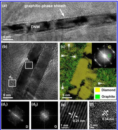
To unravel the structure of the DNW, we have completed high-resolution TEM (HRTEM) studies. Figure 3a displays an HRTEM image of a DNW, exhibiting a clear core−shell microstructure. Each DNW is found to be encased by the graphite phase, which probably forms during the growth of DNWs. The thickness of the graphitic layer varies from a few atomic layers to more than 5 nm. To analyze the two crystalline carbon phases of diamond and graphite structures in detail, another HRTEM image (Figure 3b) is taken and its corresponding Fourier transformed (FT) pattern is displayed in the inset. Moreover, the yellow and green spots on the FT diffraction pattern are inversely transformed to address the diamond (area in yellow) and graphite (area in green) phases on the HRTEM image (see Figure 3c). Such a colored HRTEM image in Figure 3c clearly indicates again that the graphitic layer (green region) encases the surface of the DNWs (yellow region). In addition to the graphitic sheath, there are a few nanometer-sized diamond grains randomly oriented near the DNW (marked as X in Figure 3c). The diamond and graphitic structures are further analyzed by FT on selected areas. Figure 3d1shows the FT pattern on d1area (marked in
Figure 3b) giving the ordering of the (111) planes of the diamond structure whereas Figure 3d2shows the FT pattern on
d2 area pointing to the ordering of the (111) planes of the graphitic structure. High-magnification HRTEM image of the d1area is offered in Figure 3e, which reflects considerably the crystalline nature with a lattice spacing of 0.21 nm. These results confirm that the DNW is encapsulated by a sheath of graphitic phase. The microstructural studies of DNW films
Figure 1.(a) Low-magnification TEM image of DNW films. The inset shows FESEM image for comparison. (b) TEM-corresponding SAED pattern, where different lattice-plane spacings of diamond are indicated. (c) visible−Raman spectrum of DNWs films. The characteristic peaks of trans-polyacetylene, diamond, and graphite bands are marked as t-PA, D, and G, respectively.
Figure 2.NEXAFS C−K edge spectrum of DNWs films. The inset shows C 1s XPS spectrum with fourfitting curves to identify carbon binding states.
confirmed that this graphitic content is formed during the growth offilms. The presence of abundant CN species in the N2/CH4 plasma, which was observable in optical emission spectra (figure not shown), may preferentially induce the formation of nanorod, along with the graphitic phase encasing the nanorods.48,49
3.2. Electrical Properties. Hall measurements in van der Pauw configuration were taken on DNWs films at the millimeter scale at RT so as to measure their electrical conductivities. The negative value of the Hall coefficients indicates that the majority of carriers are electrons in DNWs films. The carrier concentrations, electrical conductivity and mobility of the DNWs films are evaluated to be about 1.0 × 1020 cm−3, 186 S cm−1, and 11.6 cm2/V s. To scrutinize the main conducting paths for electrons from the microscopic viewpoint, CITS and STS spectra measurements were performed to obtain tunneling I−V curves on DNWs films. Figure 4a shows a typical STM image of a DNW with a length of about 200 nm. The dark area representing a valley place between DNWs is marked as DNWs interval which is the space between DNWs and is about several tens to hundreds of nanometer away from DNWs. Figure 4b presents a CITS image at a sample bias voltage of −3.75 V that corresponds to the STM image in Figure 4a. The bright and high-current region is
close to the DNWs whereas the dark and low-current region is close to the DNWs interval. Additionally, STS spectra of tunneling I−V curves at the marked position in images a and b in Figure 4 are offered in Figure 4c. The position at the DNWs interval reveals a lower current of an insulating feature while the position on DNWs exposes much higher current to indicate the effective conducting path. The feature can be observed, for example, at a given bias voltage of about 1.4 V the current difference is larger than 2 orders of magnitude. Consequently, the conducting paths are on surface of the DNWs rather than in the interval between DNWs.
The conducting paths on the surface of DNWs are inspected carefully. The zoom-in, high-resolution STM image of the surface of a single DNW is shown in Figure 4d. To examine the microstructure on the surface of the DNW, the STM image in a highly contrast mode is presented in Figure 4e for an easy identification of diamond grains and graphitic grain boundaries. The DNW is made of smaller diamond clusters of equiaxed geometry. The cluster size varies between 2.0 and 5.0 nm which is consistent with that of the diamond grains, incorporated in the conventional UNCD films grown by Ar/CH4 plasma. Apparently, the grains in the STM image (Figure 4e) are diamond grains which are adhered to get elongation of DNWs (see Figure 3c for the similar feature). In addition, Figure 4f
Figure 3.(a) HRTEM image of a single DNW disclosing the core−shell microstructure. (b) HRTEM image with its corresponding FT pattern displayed in the inset. (c) Inverse FT image from the inset of b to mark the diamond and graphite regimes. FT patterns of d1and d2areas in TEM
image b are shown infigures d1and d2, respectively. (e) Crystalline structure of the d1area in b presenting a clear (111) planes of the diamond
presents the STS spectra of tunneling I−V curves at the diamond grain (Grain) and graphitic grain boundary (GB) which are marked in Figure 4e. Very excitingly, the tunneling current at the graphitic GB position is much larger than that at the diamond Grain position. From such a microscopic inspection, this result confirms again that the electron conducting path is along the graphitic GB rather than the diamond Grain on the surface of DNWs. It is noted that the average of the two−-V curves in Figure 4f is very close to the I−V curve (marked as DNWs) manifested in Figure 4c, corroborating the rationalization of the CITS measurements. Moreover, the GB regimes surrounding the isolated Grains assist to establish conducting channels covering on the whole surface of DNWs. The size of GBs is roughly equal to the Grain size of ∼3 nm. These DNWs are randomly distributed and electrically contacted in the film to form 3D conducting channels; likewise the tunneling I−V curve at GB demonstrates a very low threshold voltage lower than 0.5 V and a tunneling current higher than 50 nA. Such a special property at GB on surface of DNWs may give superior EFE properties.
On the other hand, DNWs devices were fabricated to probe their electron transport at the hundred-nanometer scale. I−V characteristics of the DNWs device (DNW1) were obtained (Figure 5a) by sweeping currents and acquiring voltages at various temperatures. At a given voltage, the current of the
DNW1 device increases with a decrease of temperature. I−V curves are linear up to a large current of± 1 μA, indicating an Ohmic contact between the DNWs film and the Ti/Au electrode. The Ohmic contact ensures the measurement of intrinsic conductivities or resistivity of DNWs. The RT conductivity of the DNW1 device is estimated to be about 175 S cm−1which is in excellent line with that obtained by the Hall measurement. A schematic diagram of the DNWs device is depicted in the inset of Figure 5a. It is noted that the separation distance between the pairing electrodes was kept a constant for all devices. Temperature dependent behaviors of three DNWs devices (DNW1−3) are displayed in Figure 5b. The conductivity decreases with decreasing temperature which implies either a thermal activation of semiconductor or a strong localization of a disordered system. In a strong disorder system such as the graphitic phase randomly oriented in grain boundaries and encasing DNWs, electrons are localized in the fluctuated random potential. Therefore, temperature dependent conductivity can be described by the Mott’s variable range hopping (VRH) model in accordance with the expression of σ=σ0exp(−T0/T)−1/p,50 where σ and T are conductivity and
temperature,σ0is a weak temperature-dependent constant, and T0is a constant of a characteristic temperature. The exponent p
is 2, 3, or 4 for a one-, two-, or three-dimensional (3D) disordered system, respectively. Figure 5b presents the normalized conductivity of the DNWs devices in a logarithm scale showing a linear dependence on T−1/4 at temperature ranges from 300 to 20 K and complying with the Mott’s 3D VRH model. The experimental average values of σ0 and T0
derived from the bestfits to data in Figure 5b are about 20 S cm−1and 1.9× 10⁵K, respectively.
To verify the correctness of using the Mott’s 3D VRH model, we analyzed the parameters derived from thefits to our data as
Figure 4. (a) STM image DNWs films with (b) its corresponding current image at−3.75 V. The positions of the DNWs and the DNWs interval are marked. (c) The STS spectra (tunneling I−V curves) at the marked position in a and b. (d) STM image of a single DNW. (e) Its high contrast image, to discern diamond grains and grain boundaries on DNWs. (f) STS spectra of tunneling I−V curves at the marked position in e.
Figure 5. (a) I−V curves of the DNWs device (DNW1) at various temperatures. A schematic diagram of the DNWs device is drawn in the inset. (b) Temperature-dependent conductivities of three different DNWs devices (DNW1−3). The solid lines present the best fits to our data. The conductivities are normalized by dividing with its RT value for comparison with ease. (c) Hopping energy, WVRH, as a function of
temperature (red curve). The dashed line portrays the thermal energy for comparison. (d) Hopping distance, RVRH, as a function of
(3/8)ξ(T0/T) , where ξ is the localization length of electrons in DNWs films. Assuming that ξ as the size of grain boundary on surface of DNWs (about 3 nm), the hopping distance can be estimated to be in the range between 5.6 and 11 nm from 300 to 20 K (Figure 5d). Finally, the last supporting point is that the carrier density evaluated from the T0parameter
shall be in line with our previous estimation of high conductivity and carrier concentration. The characteristic temperature, T0, is described by the form T0= 18/(kBg0ξ3),50
where g0 is the density of states at Fermi level. Thus we can
evaluate g0 to be about 2.0 × 10²⁰ eV−1 cm−3. Such a high
density of states self-consistently supports our previous evaluation of a high carrier concentration as well as a high conductivity of the DNWsfilm.
3.3. Application: Electron Field Emission Source. The EFE properties of the DNWs encased by the highly conducting graphite were tested in order to demonstrate their specific applications in future electronics. Figure 6 presents emission
current density, J, as a function of the applied electricfield, E. It reveals a low turn-onfield of ∼4.35 V/μm at a current density of 3μA/cm2. In addition, the current density increases rapidly
and reaches the large magnitude of∼3.42 mA/cm2at thefield of 9.1 V/μm. In addition, the relationships among the current density (J), electric field (E), work function (φ) and field enhancement factor (β) of an emitter are expressed by the F− N equation: J = (Aβ2E2/φ) exp (−Bφ3/2/βE), where A = 1.54 × 10⁻⁶A eV V−2and B = 6.83× 10⁹eV−3/2V m−1. Wefit the
highfield segments of the F−N curve to the above equation and the results of thefitting are shown as solid line in the inset of Figure 6, illustrating that the EFE datafit the F−N model very well. We assume that theφ value of diamond is assumed as 5.0 eV51for estimating theβ value of DNWs, which is β = 1024
4. CONCLUSION
Conducting DNWsfilms with a carrier concentration of ∼1.0 × 1020 cm−3 and a conductivity of 186 S cm−1 have been
synthesized by using N2/CH4 plasma. TEM and FESEM
analyses portray the feature of nanowire morphology with a length of few hundred nanometers. The SAED pattern and visible-Raman spectrum indicate the coexistence of diamond and graphitic phases that is verified again in the NEXAFS spectrum. The XPS spectrum confirmed the introduction of nitrogen into the DNWs films. Further, the HRTEM image exposes randomly oriented diamond grains on DNWs and graphitic layer encasing the surface of DNWs. STM and STS measurements show up the insulating manner in the interval space between DNWs. It also reveals the highly conducting paths through the graphitic grain boundaries rather than the diamond grains on surfaces of DNWs. Grain boundaries establish conducting channels covering on the whole surface of the DNW and DNWs are electrically contacted to form 3D conducting channels. On the other hand, DNWsfilms, placed in the 200 nm wide gap between pairing electrodes, were employed for disclosing electron transport at nanometer scale. The temperature dependence of conductivities convinces a
Figure 6.Emission current density as a function of applied electric field for DNWs films. The data in the form of ln(J/E2)− 1/E plot are
presented in the inset. The solid line indicates a high-field approach fitting by the F−N theory.
materials (V/fieldμm) current density enhancement factor undoped nanostructured diamond52 4.9 10mA/cm2
boron doped diamond-clad si tips53
15.5 90μA/ cm2
diamond−nondiamond
compositefilms54 9.0 1.9mA/cm2
Freestanding n-type conducting UNCDfilms55
10 0.20
mA/cm2
c-diamond and n-diamond grains
on Si nanoneedles56 2.2 2.2mA/cm2 1491
vertically aligned conducting
UNCD nanorods57 2.04 4.84mA/cm2 1945
free-standing graphene−diamond hybridfilms58
2.4 0.1 mA/cm2
CNT−graphene hybrid
materials59 2.9 1.33mA/cm2 1373
open-ended tubular graphite cones60 1.8 0.65 mA/cm2 3700 coral-like CNTs61 4.0 CNT/TEOS62 1.76 0.5 mA/cm2 5607
metallic nanowire−graphene hybrid nanostructures63 7 300μA/ cm2 3533 DNWfilmsPresent study 4.35 3.42 mA/cm2 1024 figure captions
transport mechanism of the Mott’s 3D VRH model in DNWs at temperatures ranging from 300 to 20 K. This result points to the hopping demeanor of electron transport between grain boundaries and DNWs. More interestingly, the character of conducting grain boundaries on DNWs can be used to demonstrate an excellent EFE property that evidence high potential applications infield emission or plasma devices.
■
AUTHOR INFORMATIONCorresponding Author
*E-mail: [email protected] (N.H.T); [email protected]. edu.tw (I.N.L.).
Author Contributions
The manuscript was written through contributions of all authors. All authors have given approval to thefinal version of the manuscript.
Notes
The authors declare no competingfinancial interest.
■
ACKNOWLEDGMENTSThis work was supported by the Taiwan National Science Council under Grants NSC 101-2112-M-032−002-MY2 and NSC 101-2221-E-007-064-MY3.
■
REFERENCES(1) Zhu, W.; Kochanski, G. P.; Jin, S.; Seilbles, L. J. Appl. Phys. 1995, 78, 2707.
(2) de Heer, W. A.; Chatelain, A.; Ugarte, D. Science 1995, 270, 1179. (3) Amaratunga, G. A. J.; Silva, S. R. P. Appl. Phys. Lett. 1996, 68, 2529.
(4) Sun, M.; Gao, Y.; Zhi, C.; Bando, Y.; Golberg, D. Nanotechnology 2011, 22, 145705.
(5) Yamaguchi, H.; Masuzawa, T.; Nozue, S.; Kudo, Y.; Saito, I.; Koe, J.; Kudo, M.; Yamada, T.; Takakuwa, Y.; Okano, K. Phys. Rev. B 2009, 80, 165321.
(6) Geis, M. W.; Efremow, N. N.; Krohn, K. E.; Twichell, J. C.; Lszczarz, T. M.; Kalish, R.; Greer, J. A.; Tabat, M. D. Nature 1998, 393, 431.
(7) Okano, K.; Koizumi, S.; Silva, S. R. P.; Amaratunga, G. A. J. Nature 1996, 381, 140.
(8) Watanabe, H.; Nebel, C. E.; Shikata, S. Science 2009, 324, 1425. (9) Cui, Y.; Wei, Q.; Park, H.; Lieber, C. M. Science 2001, 293, 1289−1292.
(10) Huang, M. H.; Mao, S.; Feick, H.; Yan, H.; Wu, Y.; Kind, H.; Webber, E.; Russo, R.; Yang, Y. Science 2001, 292, 1897−1899.
(11) Huang, Y.; Duan, X.; Wei, Q.; Lieber, C. M. Science 2001, 291, 630−633.
(12) Rao, S. G.; Huang, L.; Setyawan, W.; Huang, S. Nature 2003, 425, 36−37.
(13) Baughman, R. H.; Zakhidov, A. A.; Heer, W. A. de. Science 2002, 297, 787−792.
(14) Iijima, S. Nature 1998, 354, 56−58.
(15) Ma, D. D. D.; Lee, C. S.; Au, F. C. K.; Tong, S. Y.; Lee, S. T. Science 2003, 299, 1874−1877.
(16) Barnard, A. S.; Russo, S. P.; Snook, I. K. Nano Lett. 2003, 3, 1323−1328.
(17) Barnard, A. S.; Snook, I. K. J. Chem. Phys. 2004, 120, 3817− 3821.
(18) Wang, C. X.; Yang, G. W. Mater. Sci. Eng., R 2005, 49, 157−202. (19) Fonoberov, V. A.; Balandin, A. A. Nano Lett. 2006, 6, 2442− 2446.
(20) Ghosh, S.; Calizo, I.; Teweldebrhan, D.; Pokatilov, E. P.; Nika, D. L.; Balandin, A. A.; Bao, W.; Miao, F.; Lau, C. N. Appl. Phys. Lett. 2008, 92, 151911.
(21) Shiomi, H. Jpn. J. Appl. Phys. 1997, 36, 7745−7748.
(22) Masuda, H.; Watanabe, M.; Yasui, K.; Tryk, D.; Rao, T.; Fujishima, A. Adv. Mater. 2000, 12, 444−447.
(23) Arenal, R.; Bruno, P.; Miller, D. J.; Bleuel, M.; Lal, J.; Gruen, D. M. Phys. Rev. B 2007, 75, 195431.
(24) Arenal, R.; Montagnac, G.; Bruno, P.; Gruen, D. M. Phys. Rev. B 2007, 76, 245316.
(25) Gruen, D. M. Annu. Rev. Mater. Sci. 1999, 29, 211−259. (26) Sankaran, K. J.; Panda, K.; Sundaravel, B.; Chen, H. C.; Lin, I. N.; Lee, C. Y.; Tai, N. H. ACS Appl. Mater. Interfaces 2012, 4, 4169− 4176.
(27) Bhattacharyya, S.; Auciello, O.; Birrell, J.; Carlisle, J. A.; Curtiss, L. A.; Goyette, A. N.; Gruen, D. M.; Krauss, A. R.; Schlueter, J.; Sumant, A.; Zapol, P. Appl. Phys. Lett. 2001, 79, 1441−1443.
(28) Birrell, J.; Gerbi, J. E.; Auciello, O.; Gibson, J. M.; Gruen, D. M.; Carlisle, J. A. J. Appl. Phys. 2003, 93, 5606−5612.
(29) Vlasov, I. I.; Lebedev, O. I.; Ralchenko, V. G.; Goovaerts, E.; Bertoni, G.; Tendeloo, G. V.; Konov, V. I. Adv. Mater. 2007, 19, 4058−4062.
(30) Chen, Y. C.; Tai, N. H.; Lin, I. N. Diamond Relat. Mater. 2008, 17, 457−461.
(31) Shang, N.; Papakonstantinou, P.; Wang, P.; Zakharov, A.; Palnitkar, U.; Lin, I. N.; Chu, M.; Stamboulis, A. ACS Nano 2009, 3, 1032−1038.
(32) Bhattacharyya, S. Phys. Rev. B 2004, 70, 125412.
(33) Beloborodov, I. S.; Zapol, P.; Gruen, D. M.; Curtiss, L. A. Phys. Rev. B 2006, 74, 235434.
(34) Shah, K. V.; Churochkin, D.; Chiguvare, Z.; Bhattacharyya, S. Phys. Rev. B 2010, 82, 184206.
(35) Mareš, J. J.; Hubίk, P.; Krištofik, J.; Kindl, D.; Fanta, M.; Nesládek, M.; Williams, O.; Gruen, D. M. Appl. Phys. Lett. 2006, 88, 092107.
(36) Bhattacharyya, S. Phys. Rev. B 2008, 77, 233407.
(37) Choy, T. C.; Somoza, A. M.; Ortuno, M.; Somoza, A. M. Appl. Phys. Lett. 2008, 92, 012120.
(38) Achatz, P.; Williams, O. A.; Bruno, P.; Gruen, D. M.; Garrido, J. A.; Stutzmann, M. Phys. Rev. B 2006, 74, 155429.
(39) Gerbi, J. E.; Auciello, O.; Birrell, J.; Gruen, D. M.; Alphenaar, B. W.; Carlisle, J. A. Appl. Phys. Lett. 2003, 83, 2001−2003.
(40) Fowler, R. H.; Nordheim, L. Proc. R. Soc. London, Ser. A 1928, 119, 173−181.
(41) Thomsen, C.; Reich, S. Phys. Rev. Lett. 2000, 85, 5214. (42) Ferrari, A. C.; Robertson, J. Phys. Rev. B 2001, 63, 121405. (43) Kuzmany, H.; Pfeiffer, R.; Salk, N.; Günther, B. Carbon 2004, 42, 911−917.
(44) Vlasov, I. I.; Ralchenko, V. G.; Goovaerts, E.; Saveliev, A. V.; Kanzyuba, M. V. Phys. Status Solidi (a) 2006, 203, 3028−3035.
(45) Chang, Y. K.; Hsieh, H. H.; Pong, W. F.; Tsai, M. H.; Chien, F. Z.; Tseng, P. K.; Chen, L. C.; Wang, T. Y.; Chen, K. H.; Bhusari, J. R.; Yang, J. R.; Lin, S. T. Phys. Rev. Lett. 1999, 82, 5377−5380.
(46) Joseph, P. T.; Tai, N. H.; Chen, C. H.; Niu, H.; Cheng, H. F.; Pong, W. F.; Lin, I. N. J. Phys. D: Appl. Phys. 2009, 42, 105403.
(47) Chen, Y. F. Surf. Sci. 1997, 380, 199−209.
(48) Sankaran, K. J.; Kurian, J.; Chen, H. C.; Dong, C. L.; Lee, C. Y.; Tai, N. H.; Lin, I. N. J.Phys. D: Appl. Phys. 2012, 45, 365303.
(49) Teii, K.; Ikeda, T. Diamond Relat. Mater. 2007, 16, 753−756. (50) Mott, N. F. Conduction in Non-crystalline Materials; Clarendon Press: Oxford, U.K., 1993; p 32.
(51) Liu, J.; Zhirnov, V. V.; Myers, A. F.; Wojak, G. J.; Choi, W. B.; Hren, J. J.; Wolter, S. D.; McClure, M. T.; Stoner, B. R.; Glass, J. T. J. Vac. Sci. Technol. B 1995, 13 (2), 422−426.
(52) Zhu, W.; Kochanski, G. P.; Jin, S. Science 1998, 282, 1471−1473. (53) Tarntair, F. G.; Chen, L. C.; Wei, S. L.; Hong, W. K.; Chen, K. H.; Cheng, H. C. J. Vac. Sci. Technol. B 2000, 18, 1207−1211.
(54) Pradhan, D.; Lin, I. N. ACS Appl. Mater. Interfaces 2009, 1, 1444−1450.
(55) Thomas, J. P.; Chen, H. C.; Tai, N. H.; Lin, I. N. ACS Appl. Mater. Interfaces 2011, 3, 4007−4013.
T. Appl. Phys. Lett. 2003, 81, 5024−5026.
(62) Jeong, H. J.; Jeong, H. D.; Kim, H. Y.; Kim, J. S.; Jeong, S. Y.; Han, J. T.; Bang, D. S.; Lee, G. W. Adv. Funct. Mater. 2011, 21, 1526− 1532.
(63) Arif, M.; Heo, K.; Lee, Yang, B.; Lee, J.; Seo, D. H.; Seo, S.; Jian, J.; Hong, S. Nanotechnology 2011, 22, 355709.
(64) Wang, Q. H.; Setlur, A. A.; Lauerhaas, J. M.; Dai, J. Y.; Seeling, E. W.; Chang, R. P. H. Appl. Phys. Lett. 1998, 72, 2912−2913.