國 立 交 通 大 學
電子工程學系 電子研究所 碩士班
碩 士 論 文
利用一倍供應電壓元件實現二倍供應電壓
共容輸入輸出緩衝器設計
Design of 2xVDD-Tolerant I/O Buffer
with 1xVDD CMOS Devices
研 究 生:林彥良
指導教授:柯明道 教授
利用一倍供應電壓元件實現二倍供應電壓
共容輸入輸出緩衝器設計
Design of 2xVDD-Tolerant I/O Buffer
with 1xVDD CMOS Devices
研 究 生:林彥良 Student:Yan-Liang Lin
指導教授:柯明道 教授 Advisor:Ming-Dou Ker
國立交通大學
電子工程學系
電子研究所
碩士論文
A ThesisSubmitted to Department of Electronics Engineering & Institute of Electronics College of Electrical and Computer Engineering
National Chiao Tung University in Partial Fulfillment of the Requirements
for the Degree of Master
in
Electronics Engineering August 2009
Hsinchu, Taiwan, Republic of China
i
利用一倍供應電壓元件實現二倍供應電壓
共容輸入輸出緩衝器設計
學生: 林彥良
指導教授: 柯 明 道 教授
國立交通大學
電子工程學系 電子研究所碩士班
摘要
隨著互補式金氧半導體(Complementary Metal-Oxide-Semiconductor, CMOS) 積體電路製程技術的演進,電晶體閘極氧化層(gate-oxide)的厚度越來越薄,其 所能承受的最大跨壓,包括閘極-源極電壓(Vgs)和閘極-汲極電壓(Vgd)也跟著 變小。為增快電路的工作速度,以及降低能源的消耗,近來的積體電路設計所 使用之工作電壓也跟著降低。然而較早的CMOS 製成技術所設計的電路,使用 相 對 於 先 進 製 程 所 能 忍 受 的 較 大 工 作 電 壓 。 混 合 電 壓 輸 出 入 緩 衝 器 (mixed-voltage I/O buffer)作為不同電壓之傳輸介面,如何避免閘極氧化層過壓 (gate-oxide overstress)以提高積體電路的使用壽命,是一項重要的課題。此外電 路的操作速度越來越快,如何降低接地彈跳(ground bounce)的影響,也是一個 特別的挑戰。更進一步地,為確保訊號的完整性和維持電路速度上的表現,輸 出入緩衝器必須使電壓迴轉率(slew rate)的變異量越小越好。 在本篇論文當中,提出了一個使用一倍供應電壓元件的一個二倍供應電壓共 容輸入輸出緩衝器,且驗證於0.18μm CMOS 製程技術,伴隨動態源極輸出技術
ii
(dynamic source output technique)和新閘極控制電路(new gate-controlled circuit), 其可以傳送及接收二倍供應電壓之訊號且不會發生閘極氧化層過壓的問題。此新 提出之二倍供應電壓共容輸入輸出緩衝器可在不同的 CMOS 製程下實現,以滿 足不同的混合電壓介面之應用。 在論文的後半,將此新提出之二倍供應電壓共容輸入輸出緩衝器結合電壓迴 轉率控制(slew-rate control)電路,以降低接地彈跳的影響。此外,此新提出之二 倍供應電壓共容輸入輸出緩衝器也結合了製程、電壓及溫度補償(process, voltage, and temperature compensation)電路,使電壓迴轉率(slew rate)的大小在不同的環境 下,仍能維持在一定的範圍以內。
iii
Design of 2xVDD-Tolerant I/O Buffer
with 1xVDD CMOS Devices
Student: Yan-Liang Lin
Advisor: Prof. Ming-Dou Ker
Department of Electronics Engineering & Institute of Electronics
National Chiao-Tung University
ABSTRACT
With the advance of complementary metal-oxide-semiconductor technology, the gate-oxide of the transistor becomes thinner and the maximum voltage across the gate-oxide including gate-source voltage (Vgs), gate-drain voltage (Vgd) of the MOS transistor has decreased drastically. In order to increase the operating speed and decrease the power consumption, the supply voltage of recent design of an integrated circuit has been decreased. However, the earlier defined standards or interface protocols of CMOS ICs use the supply voltage higher than the advanced CMOS process. The mixed-voltage I/O buffer acts the interface of different voltage levels, so the avoidance of gate-oxide overstress to extend the circuit’s life time is an important issue in nanoscale technology. In addition, the ground bounce effects get worse with increasing operating speed. It also presents special challenges for I/O designers. Furthermore, to ensure the validity of signals and maintain the operating speed, it is another important issue to keep the output slew-rate as constant as possible.
iv
devices has been proposed and verified in a 0.18-μm CMOS process. With the dynamic source output technique and the new gate-controlled circuit, the new proposed I/O buffer can transmit and receive the signals with the voltage swing twice as high as the normal power supply voltage (VDD) without suffering gate-oxide reliability problem. The proposed 2xVDD-tolerant I/O circuit solution can be implemented in different nanoscale CMOS processes to meet the mixed-voltage interface applications in microelectronic systems.
Furthermore, to reduce the ground bounce effects, the new 2xVDD-tolerant I/O buffer is combined with the slew-rate control circuit. In addition, the new 2xVDD-tolerant I/O buffer is also combined with PVT compensation circuit to make the output slew rate as constant as possible.
v
ACKNOWLEDGEMENTS
致謝
在這兩年的碩士生涯當中,首先我要感謝的是我的指導教授 柯明道老師。 在老師身上,我看到了什麼叫做「男人」。開會時,老師經常要面對我們十幾個 同學的車輪戰,有時開會開到三更半夜,我們都已經累垮了,老師卻仍能精神奕 奕地指導我們,分析所有的問題,讓我體會到人體的極限,原來能延展到這種地 步。老師在接了義守大學副校長職位之後,變得更加忙碌,卻不辭辛苦的南北兩 地奔波,老師的處事態度,是我一輩子的指標。 而在我的研究過程中,我要感謝「奈米與晶片系統實驗室」的各位,帶我的 陳世範學長,從一開始我什麼都不懂的時候,一步步地帶我入門,連趕在畢業前 夕,仍熱心地幫我解決問題。廖期聖學長在研究、學業及生活上,給予我的幫助, 可以寫的比這篇論文還長,我的命說是他給的也不為過。在一些學長相繼畢業之 後,陸亭州學長一肩扛下了所有的責任,喜歡唱「壞人」的他,像個好人一樣地 帶領了好幾個學弟妹順利畢業。而顏承正學長則如菩薩轉世,即便學業及生活的 壓力接踵而至時,仍能散發出慈愛的光芒,庇蔭著實驗室的芸芸眾生,其戰鬥力 之高,也不是我所能想像的。另外蕭淵文、王資閔、林群佑、陳穩義、陳世宏、 邱柏硯、陳紹岐、蔡惠雯等學長姐,在各方面給予我協助,讓我可以順利完成我 的畢業論文。 再來感謝社交魔人肉昀、道德魔人天天、左手的阿戴爾、送咧的 kitty、補 刀的育祥、教練溫董、黑肉底的阿官、唉呦沒差的彥緯、團購的翁姐、愛講不討 喜的佳琪、鼎王的世昕、很難見到的小賴、笑將科科、損毀我形象的小凡、PCB 魔人歐文、不意外的歐陽、不會騙人的宗恩、爆雷的宅哥,兩年碩士,有你們一 起研究,一起玩樂,一起做好事,一起做壞事,我覺得很幸運,也很幸福。另外 感謝我親愛的學弟們,狗達的朋友癡癡、癡癡的朋友狗達、可愛的糖糖(糖糖是 男生)、包皮爾斯的偉霖,你們都是實驗室的希望。 最後,要感謝的是我的父親林銘鋒先生、母親張月女女士、大哥林彥甫、二 哥林彥彣以及我的女友文琪。家人給我的支持,讓我可以無後顧之憂的完成學 業,在我感到徬徨時,也能給我意見與協助,是我最強硬的後盾。而女友在我開 心時,分享我的喜悅,在我消極無助時,更是默默地陪在我身邊,鼓勵我,讓我 能堅強地站起來。你們的支持,是我堅持下去最重要的動力,謝謝你們。 要感謝的人太多了,若有遺漏,在此一併謝過。本論文撰寫時已力求嚴謹, 然謬誤之處在所難免,尚祈各位讀者不吝惜賜予寶貴意見,使本論文能更加完善。 林 彥 良 僅誌於竹塹交大 民國九十八年八月vi
CONTENTS
ABSTRACT (CHINESE) ... i
ABSTRACT (ENGLISH) ... iii
ACKNOWLEDGEMENTS ... v
CONTENTS... vi
TABLE CAPTIONS ... viii
FIGURE CAPTIONS ... ix
Chapter 1 Introduction ... 1
1.1 Motivation ... 1
1.2 I/O Buffer Basics ... 2
1.3 Gate-Oxide Overstress Problem ... 3
1.4 Thesis Organization... 3
Chapter 2 Prior Design ... 5
2.1 Prior Design I: The Mixed-Voltage I/O Buffer with Gate-Tracking Circuit and Dynamic N-WELL Bias Circuit ... 5
2.2 Prior Design II: The Mixed-Voltage I/O Buffer with Blocking NMOS Technique ... 7
Chapter 3 New 2xVDD-Tolerant I/O Buffer ... 10
3.1 Introduction ... 10
3.2 Implementation of Proposed 2xVDD-Tolerant I/O Buffer ... 10
3.2.1 Design Concept ... 10
3.2.2 Circuit Scheme and Operation Modes ... 12
3.2.3 Gate-Controlled Circuit ... 14
3.2.4 Level Converter ... 15
3.2.5 Discussions... 17
3.3 Simulation Results ... 17
3.3.1 Function of Proposed 2xVDD-Tolerant I/O Buffer ... 17
3.3.2 Slew Rate Effects of Input Signal in Receive Mode ... 19
3.3.3 Discussion of Propagation Delay with Gate-Controlled Circuit ... 22
3.4 Experimental Results ... 23
3.4.1 Measurement Settings ... 23
vii
Chapter 4 New 2xVDD-Tolerant I/O Buffer with Slew-Rate Control ... 29
4.1 Introduction ... 29
4.2 Traditional Output Buffer with Slew-Rate Control ... 30
4.3 New 2xVDD-Tolerant I/O Buffer with Slew-Rate Control ... 31
4.3.1 Circuit Implementation ... 31
4.3.2 Simulation Results ... 33
4.3.3 Ground Bounce ... 35
Chapter 5 New 2xVDD-Tolerant I/O Buffer with PVT Compensation ... 40
5.1 Introduction ... 40
5.2 New 2xVDD-Tolerant I/O Buffer with PVT Compensation ... 41
5.2.1 PVT Variation Detector ... 41
5.2.2 Encoder ... 43
5.2.3 Output Stage with Control Signals ... 45
5.3 Proposed 2xVDD-Tolerant Logic gate ... 47
5.4 Simulation Results ... 52
5.4.1 Simulation Results with 3-bits control signals ... 52
5.4.2 Simulation Results with 4-bits control signals ... 55
Chapter 6 Conclusions and Future Works ... 58
6.1 Conclusions ... 58
6.2 Future Works ... 59
viii
TABLE CAPTIONS
Table 2.1The operations of the mixed-voltage I/O buffer with blocking NMOS. ... 7 Table 3.1Operation Modes of the new proposed 2xVDD-tolerant I/O buffer. ... 14 Table 3.2The relation between the propagation delay and the power consumption. .. 23 Table 4.1 The size ratio of the output transistors ... 33 Table 4.2 The simulation results of new 2xVDD-tolerant I/O buffer with or
without slew-rate control. ... 34 Table 5.1Truth table of Encoder in the PVT compensation circuit. ... 44 Table 5.2The size ratios of the output driver. ... 46 Table 5.3The slew rate of the I/O PAD of the new 2xVDD-tolerant I/O buffer
without PVT compensation. ... 53 Table 5.4The shmoo plot of the outputs of 8-to-3 encoder. ... 54 Table 5.5 The slew rate of the I/O PAD of the new 2xVDD-tolerant I/O buffer
with PVT compensation using 3-bits control signals. ... 55 Table 5.6The shmoo plot of the outputs of 16-to-4 encoder. ... 56 Table 5.7The slew rate of the I/O PAD of the new 2xVDD-tolerant I/O buffer with
ix
FIGURE CAPTIONS
Fig. 1.1 Reliability issues on the conventional I/O buffer. ... 2 Fig. 2.1 Design concept for traditional mixed-voltage I/O buffer realized with only
thin-oxide devices [4]. ... 6 Fig. 2.2 The mixed-voltage I/O buffer with a blocking NMOS and a dynamic
gate-bias circuit. ... 8 Fig. 2.3 Circuit implementation of the dynamic gate-bias circuit in Fig. 2.2. ... 9 Fig. 3.1 The operations of the output stage in a 2xVDD-tolerant I/O buffer in
transmit mode with (a) transmitting high and (b) transmitting low. ... 11 Fig. 3.2 The operations of the output stage in a 2xVDD-tolerant I/O buffer in
receive mode with (a) receiving high and (b) receiving low. ... 11 Fig. 3.3 The new proposed 2xVDD-tolerant I/O buffer. ... 13 Fig. 3.4 The gate-controlled circuit for the new proposed 2xVDD-tolerant
I/O buffer. ... 15 Fig. 3.5 The modified level converter which represents the level converter
shown in Fig. 3.3 and Fig. 3.4. ... 16 Fig. 3.6 Simulated waveforms of the proposed 2xVDD-tolerant I/O buffer with
133-MHz signals in (a) transmit mode, and (b) receive mode. ... 19 Fig. 3.7 The simulation results of the current waveforms for MP and MN in the
receive mode with the (a) 0.2-ns input rise time/fall time and (b) 1-ns
input rise time/fall time. ... 20 Fig. 3.8 The simulation results of the gate-to-source and gate-to-drain voltage
waveforms for MP and MN in the receive mode with (a) 0.2-ns input rise time/fall time and (b) 1-ns input rise time/fall time. ... 22 Fig. 3.9 The layout and die photo of the proposed 2xVDD-tolerant I/O buffer. ... 24 Fig. 3.10 The printed circuit board (PCB) of tested 2xVDD-tolerant I/O buffer. ... 24 Fig. 3.11 The measurement settings of the proposed 2xVDD-tolerant I/O buffer
in (a) transmit mode and (b) receive mode. ... 25 Fig. 3.12 The measured waveforms of the proposed I/O buffer in transmit mode
with respect to (a) 1-MHz and (b) 133-MHz I/O signals. ... 27 Fig. 3.13 The measured waveforms of the proposed I/O buffer in receive mode
with respect to (a) 1-MHz and (b) 133-MHz I/O signals. ... 28 Fig. 4.1 Conventional output buffer with slew-rate control. ... 31 Fig. 4.2 New 2xVDD-tolerant I/O buffer with slew-rate control. ... 32 Fig. 4.3 Simulation waveforms of the new 2xVDD-tolerant I/O buffer with
x
slew-rate control operating at 133 MHz when transmitting 0V-to-1.5V output signals to I/O PAD. ... 34 Fig. 4.4 Simulated model of ground bounce. ... 36 Fig. 4.5 Simulation waveforms of ground bounce effects on (a) VDDH power
line and (b) VSS power line. ... 37 Fig. 4.6 Simulation waveforms of the 2xVDD-tolerant I/O buffer with slew-rate
control for ground bounce effect in transmit mode. ... 37 Fig. 4.7 The relation between ground bounce on VDDH power line and wire bond
inductance on the new 2xVDD-tolerant I/O buffer with or without slew-rate control. (a) The overshoot and (b) the undershoot on VDDH power line. ... 38 Fig. 4.8 The relation between ground bounce on VSS power line and wire bond
inductance on the new 2xVDD-tolerant I/O buffer with or without slew-rate control. (a) The overshoot and (b) the undershoot on VSS power line. ... 39 Fig. 5.1 Block diagram of solution for PVT compensation. ... 41 Fig. 5.2 The PVT variation detector. ... 42 Fig. 5.3 The pulse triggered D flip-flop using as the register in the PVT variation
detector. ... 43 Fig. 5.4 The circuit schematic of encoder. ... 44 Fig. 5.5 The schematic of new 2xVDD-tolerant I/O buffer with PVT compensation. 46 Fig. 5.6 The schematic of new 2xVDD-tolerant I/O buffer with PVT compensation
of 4-bit control signals. ... 47 Fig. 5.7 The 2xVDD-tolerant inverter. ... 48 Fig. 5.8 The level converter being used in the 2xVDD-tolerant I/O logic gates
and the encoder circuit which is shown in Fig. 5.4. ... 49 Fig. 5.9 The implementations of 2-input 2xVDD-tolerant logic gates.
(a) The inputs (b) NAND gate, and (c) NOR gate. ... 51 Fig. 5.10 The implementations of 3-input 2xVDD-tolerant logic gates.
1
Chapter 1
Introduction
1.1
Motivation
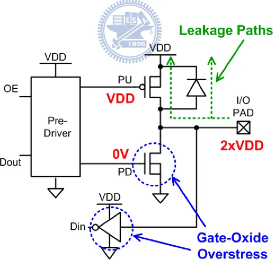
With the trend of present CMOS technologies, the transistor’s dimension has been scaled down towards nanometer region to reduce the silicon cost and increase operating speed. The thickness of gate oxide also becomes much thinner to reduce the core power supply voltage (VDD) for resulting in lower power consumption. Therefore, the maximum tolerable voltage across the transistor terminals should be correspondingly decreased to ensure lifetime. However, with compatibility to the interface protocols of CMOS integrated circuits in a microelectronics system, the chips fabricated in the advanced CMOS processes will face to the interface of signals with voltage levels higher than their normal supply voltage (VDD). In such mixed-voltage I/O interfaces, the integrated circuit may suffer the gate-oxide overstress [1] [2] and undesired circuit leakage issues [3], so a mixed-voltage I/O buffer must be designed to overcome these problems carefully.
In high-speed interface, the channel widths of output buffer are always increased to have high driving capacity, which results in large power/ground noise due to outputs swing simultaneously. The power/ground noise destroys the signals’ validity. Therefore, the output buffer must be designed with considerations of power/ground noise to achieve high performance. Furthermore, in order to both maintain the switching noise performance and timing specifications of an I/O buffer across all PVT corners, the output slew rates should be well controlled as the PVT condition varies.
2
1.2
I/O Buffer Basics
The basic structure for an I/O buffer typically includes a pre-driver, several large transistors to charge or discharge the output terminal, and an input unit, as shown in Fig. 1.1. The circuit operating modes controlled by an enable signal OE include a receive mode (for receiving an input signal) and a transmit mode (for transmitting an output signal corresponding to the data signal Dout). However, when receiving an 2xVDD input signal at the I/O PAD for the application of mixed-voltage interface, the conventional structure suffers reliability problems such as gate-oxide overstress and leakage paths from I/O PAD to the VDD through the drain to source and drain to bulk (parasitic pn junction) of the main driving PMOS transistor [4]. To overcome above problems, the solutions of prior designs will be illustrated in chapter 2.
3
1.3
Gate-Oxide Overstress Problem
With the advantages in speed, power and cost, thin-oxide devices are more suitable in high-speed and low-power applications. However, thin gate oxide with large gate-to-source voltage is vulnerable to gate-oxide breakdown. The breakdown can happen instantaneously or over time [5], [6]. The lifetime of gate oxide over the voltage stress can be expressed as equation 1-1 [5].
( )
0 01
exp
1,
BDG X
effdt
Vox t
t
τ
⎛
∗
⎞
−
∗ =
⎜
⎟
⎜
⎟
⎝
⎠
∫
(1-1),where τ0 and G are two constants, Xeff is the effective thickness of the gate oxide due to the defeats, and Vox(t) is the time-dependent voltage across the gate oxide. As expressed in equation 1-1, the larger voltage across the gate oxide or the thinner gate oxide decreases the device’s life time. Because the accumulation of the voltage stress over time determines the gate-oxide breakdown, the damage caused by transient overstress is still non-ignorable if it happens frequently and lasts for enough time. To ensure the life time of transistors, the absolute value of gate-to-source and gate-to-drain voltage should be less than the normal supply voltage
1.4
Thesis Organization
Chapter 1 describes the motivation and the reliability issues on a conventional I/O buffer. In chapter 2, two prior designs of mixed-voltage I/O buffers will be introduced. These two prior mixed-voltage I/O buffers can receive 2xVDD signals but only transmit 1xVDD signals without suffering gate-oxide overstress issue. Therefore, a new 2xVDD-tolerant I/O buffer which can transmit and receive 2xVDD signals without suffering gate-oxide overstress issue will be proposed in chapter 3. The
4
simulation and experimental results are also shown in this chapter. In chapter 4, the new 2xVDD-tolerant I/O buffer proposed in chapter 3 is redesigned with slew-rate control to decrease the ground bounce effects. Finally, in order to keep the output slew rate as constant as possible for maintaining the timing specifications and the noise performance, the new 2xVDD-tolerant I/O buffer combined with the PVT compensation circuit will be illustrated in chapter 5.
5
Chapter 2
Prior Design
2.1 Prior Design I:
The Mixed-Voltage I/O Buffer with Gate-Tracking Circuit and Dynamic N-WELL Bias Circuit
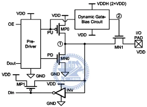
Fig. 2.1 shows the design concept of the traditional mixed-voltage I/O buffer which can receive input signals of higher voltage and transmit 1xVDD output signals [4]. It realized with thin oxide devices, a dynamic n-well bias circuit, and a gate-tracking circuit. The stacked nMOS devices, MN0 and MN1, are used to avoid the high-voltage overstress on their gate oxide. When the input signal at the I/O PAD is with the higher voltage (2xVDD) in the receive mode, the source voltage of MN0 will be VDD-Vt (where the Vt is the threshold voltage of MN0). Hence, the gate to drain voltage and the gate to source voltage of transistors MN0 and MN1 are limited below one normal power supply voltage (VDD). Thus, the stacked nMOS devices, MN0 and MN1, can solve the gate-oxide reliability problem.
The gate-tracking circuit shown in Fig. 2.1 is used to prevent the leakage current path due to the incorrect conduction of the p-channel device MP0 when the input signal at the I/O PAD is higher than VDD. In transmit mode, the gate-tracking circuit transfers the signal from the pre-driver circuit to the gate terminal of MP0. In the receive mode with 2xVDD input signal, to avoid the leakage current from the I/O PAD to the power supply (VDD), the gate-tracking circuit will bias the gate terminal of MP0 at 2xVDD to turn MP0 off completely. On the other hand, when the input signal at the I/O PAD is 0V in the receive mode, the gate-tracking circuit will keep the
6
gate terminal of MP0 at VDD to turn MP0 off completely.
The dynamic n-well bias circuit shown in Fig. 2.1 is designed to prevent the leakage current path due to the parasitic pn-junction diode in the p-channel transistor MP0. In the transmit mode, the dynamic n-well bias circuit must keep the floating n-well bias at VDD. In the receive mode with a 2xVDD input signal, the dynamic n-well bias circuit will bias the floating n-well at 2xVDD to prevent the leakage current from the I/O PAD to the power supply (VDD) through the parasitic pn-junction diode. When the input signal at the I/O PAD is 0V, the dynamic n-well bias circuit will bias the floating n-well at VDD.
In the input stage, transistor MN2 is used to make the input node of the inverter INV be VDD-Vt when the input signal at the I/O PAD is 2xVDD. Then, transistor MP1 is used to pull up the input node of inverter INV to VDD when the output node of inverter INV is pulled down to 0V. Therefore, the gate-oxide reliability problem of the input buffer can be solved.
Fig. 2.1 Design concept for traditional mixed-voltage I/O buffer realized with only thin-oxide devices [4].
7
2.2 Prior Design II:
The Mixed-Voltage I/O Buffer with Blocking NMOS Technique
Fig 2.2 shows the mixed-voltage I/O buffer with a blocking NMOS and a dynamic gate-bias circuit proposed in [7]. The VDDH shown in Fig. 2.2 is a voltage level of 2xVDD which can be generated by a charge pump circuit [8]. Transistor MN1 is the blocking NMOS that can protect the conventional I/O buffer from the high-voltage overstress. The operations of the I/O buffer with blocking NMOS are listed in Table 2.1. When the I/O buffer is operated in the receive mode, the gate terminal of MN1 (node 2) is biased at VDD by the dynamic gate-bias circuit. At the same time, the pull-high PMOS MP0 and the pull-down NMOS MN0 are both turned off by the pre-driver circuit. And then if an input signal of logic low (0V) is received from the I/O PAD, node 1 is discharged to 0V through the transistor MN1, and this input signal can be successfully transferred to the node Din. When a signal of logic high (VDDH) is received at the I/O PAD, the gate terminal of MN1 is still biased at VDD, so the voltage on node 1 will be VDD-Vt. Then, MP1 is used to restore the voltage on node 1 to VDD. With such design, MN1, MP1 and INV can convert the VDDH input signal to VDD signal successfully.
Table 2.1
8
In transmit mode, when the I/O buffer transmits the output signal of logic high (VDD), the gate terminal of MN1 (node 2) is biased at VDDH by the dynamic gate-bias circuit, so the VDD signal can be transferred to the I/O PAD successfully. When the I/O buffer is operated in the transmit mode and transmits the output signal of logic low (0V), the gate terminal of MN1 (node 2) is biased at VDD by the dynamic gate-bias circuit to avoid the MN1 suffering gate-oxide overstress issue.
Fig. 2.2 The mixed-voltage I/O buffer with a blocking NMOS and a dynamic gate-bias circuit.
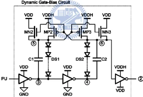
Fig. 2.3 depicts the dynamic gate-bias circuit of the I/O buffer shown in Fig. 2.2. When the voltage on node 5 is lower than VDD-Vt, MP3 will be turned on to bias node 6 at VDDH. Then, MN2 is turned on to keep the node 5 at VDD. Capacitors C1 and C2 are used to couple the signals from node 3 and 4 to node 5 and 6, respectively. Since the voltage levels on the top plate and bottom plate of capacitors C1 and C2 are either VDD and 0V or 2xVDD and VDD, the voltage across these capacitors are always VDD. With these capacitors, when node 3 converts the voltage level from
9
VDD to 0V, the voltage level on node 5 is pulled down to VDD and then the voltage on node 6 is pulled high to 2xVDD by transistor MP3. On the contrary, when node 4 converts the voltage level from VDD to 0V, the voltage level on node 6 is pulled down to VDD and then the voltage on node 5 is pulled high to 2xVDD by transistor MP2. The diode strings DS1 and DS2 are designed to a little higher than VDD by using multiple diodes in stacked configuration, so the voltage across C1 and C2 can be maintained at VDD closely. For example, if node 3 is at 0V and node 4 is VDD initially, the voltage on node 5 is clamped at the turn-on voltage (~VDD) of DS1. Therefore, MP3 is turned on to pull up the voltage on node 6 to 2xVDD. Thus, the voltage across C1 and C2 are both VDD.
Fig. 2.3 Circuit implementation of the dynamic gate-bias circuit in Fig. 2.2.
The prior designs of the mixed-voltage I/O buffer can receive 2xVDD input signals but only transmit VDD output signals. Therefore, a new 2xVDD-tolerant I/O buffer which can both transmit and receive 2xVDD signals is proposed and illustrated in the next chapter.
10
Chapter 3
New 2xVDD-Tolerant I/O Buffer
3.1
Introduction
With the rapid development of CMOS techniques, the power supply voltage (VDD) is reduced for low-power applications and the thickness of gate oxide has been scaled down to increase circuit operating speed. In the meanwhile, the maximum tolerable voltage across the transistor terminals should be decreased to ensure lifetime. However, the chips may receive the I/O signals with voltage levels higher than their normal supply voltage (VDD) from the old interface protocols of other CMOS ICs in a microelectronic system with multiple/different power supply voltages. Thus, it becomes more important to prevent the thin gate oxide of the I/O circuits in IC from voltage overstress in such mixed-voltage microelectronic systems. Recently, several mixed-voltage I/O buffers realized with thin oxide devices to receive input signals of higher voltage but only to transmit 1xVDD output signals were reported in [4], [9]-[13]. In this thesis, a 2xVDD-tolerant I/O buffer which can transmit and receive 2xVDD I/O signals without suffering gate-oxide reliability problem is proposed.
3.2 Implementation of Proposed 2xVDD-Tolerant I/O Buffer
3.2.1 Design Concept
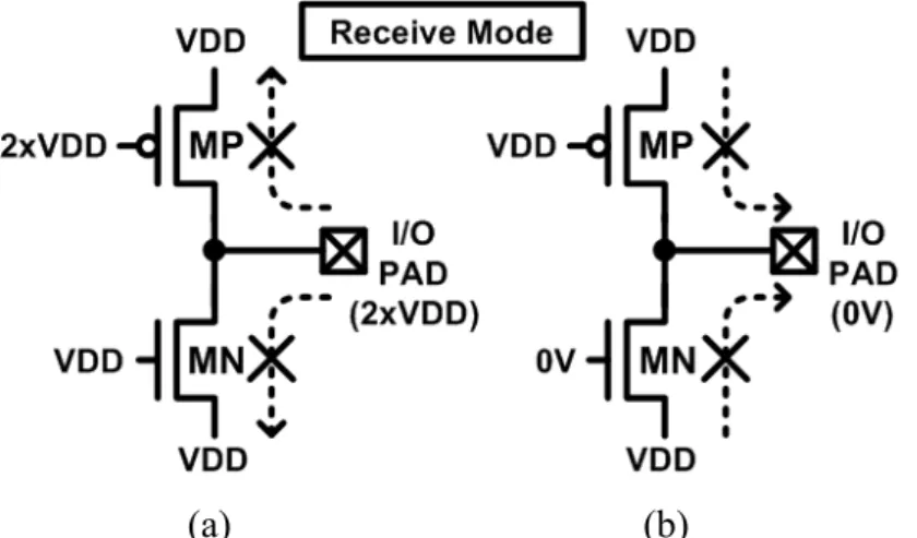
Fig. 3.1 and Fig. 3.2 show the design concept of the dynamic source output technique. MP and MN are the transistors of the output stage in an I/O circuit. As shown in Fig. 3.1 (a), when transmitting the signal high (2xVDD), the 2xVDD voltage at I/O PAD must come from the source of transistor MP. The gate voltage of
11
MP should keep MP on and keep the voltage across gate to source and gate to drain within the normal power supply voltage (VDD), so the gate voltage of MP must be VDD. At the same time, the gate voltage of MN must be also VDD to keep the voltage across gate to drain within VDD, and the source voltage of MN should be VDD to turn MN off. By the similar analysis, when transmitting the signal low (0V), the voltages at each terminal can be derived as shown in Fig. 3.1 (b). Comparing Fig. 3.1 (a) and Fig. 3.1 (b), it can be discovered that no matter transmitting high or low, the gate voltages of transistors MP and MN won’t change but their source voltages would change. Therefore, it provides us an idea to control the transistors MP and MN on or off by changing their source voltage in the transmit mode.
(a) (b)
Fig. 3.1 The operations of the output stage in a 2xVDD-tolerant I/O buffer in transmit mode with (a) transmitting high and (b) transmitting low.
(a) (b)
Fig. 3.2 The operations of the output stage in a 2xVDD-tolerant I/O buffer in receive mode with (a) receiving high and (b) receiving low.
12
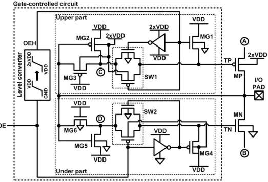
Fig. 3.2 shows the operations of the output stage in the 2xVDD-tolerant I/O buffer during receive mode. In receive mode, the devices of output stage should be kept completely off to avoid any unnecessary circuit leakage path. According to the operations in receive mode, the control signals from pre-driver will make the source voltages of MP and MN at VDD. As shown in Fig. 3.2 (a), when I/O PAD receiving 2xVDD input signal, the gate voltage of transistor MP should be biased at 2xVDD, and the gate of MN should be kept at VDD, to fully turn them off without suffering gate oxide reliability problem. With the same design consideration, the gate voltages of MP and MN can be arranged as that shown in Fig. 3.2 (b) when I/O PAD receiving signal low (0V). Observing the above analysis, it can be discovered that there needs a gate-controlled circuit whose outputs depend on the signals of OE and I/O PAD, where OE is the control signal that decides the I/O circuit operates in transmit mode or receive mode. The implementations of the dynamic source output technique and the gate-controlled circuit are shown in Fig. 3.3 and Fig. 3.4 respectively.
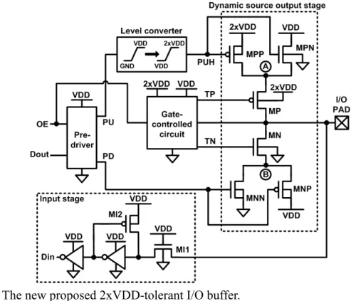
3.2.2 Circuit Scheme and Operation Modes
Fig. 3.3 shows the whole circuit scheme of the proposed 2xVDD-tolerant I/O buffer with the dynamic source output technique and the new gate-controlled circuit to protect the I/O buffer realized with 1xVDD devices against gate oxide reliability during transmitting and receiving 2xVDD signals. In transmit mode, according to the above analysis, the gate-controlled circuit biases the gate voltages TP and TN of transistors MP and MN at VDD, and then the dynamic source output stage controls the transistors MP and MN to be on or off by changing their source voltages. When the I/O buffer transmits 2xVDD output signal, PUH is pulled down to VDD by the level converter which is implemented with all 1xVDD devices. Then, the voltage at node A is 2xVDD due to the conduction of transistor MPP while MPN is off. At the
13
same time, PD is pulled down to 0V, and the voltage at node B is VDD since transistor MNP is on while MNN is off. Consequently, the I/O PAD is pulled high to 2xVDD. The similar operation for the I/O buffer to transmit 0-V output signal can be derived. In receive mode, the signals from PU and PD will control the voltages at node A and node B to VDD, and then the gate-controlled circuit provides appropriate voltages to TP and TN to completely turn MP and MN off. When the I/O buffer receives 2xVDD input signal, TP is biased at 2xVDD and TN is biased at VDD. When the I/O buffer receives 0-V input signal, TP is biased at VDD and TN is biased at 0V. Accordingly, MP and MN can be completely turned off. The corresponding circuit operating voltages of the proposed 2xVDD-tolerant I/O buffer in two operating modes are summarized in Table 3.1.
To avoid leakage current of the parasitic pn-junction diode in p-channel transistors, the bulks of transistors MP and MPP which are related to 2xVDD signals are connected to 2xVDD, and the bulks of transistors MNP and MI2 which are only related to VDD signals are connected to VDD for the concern of driving capacity.
14
Table 3.1
Operation Modes of the new proposed 2xVDD-tolerant I/O buffer.
3.2.3 Gate-Controlled Circuit
Fig. 3.4 shows the implementation of the gate-controlled circuit with 1xVDD devices which can provide appropriate voltages to the gates of MP and MN. The gate-controlled circuit can be divided into an upper part and an under part, which are with the complementary structures. All the voltage swing in the upper part are VDD-to-2xVDD, and all the voltage swing in the under part are 0V-to-VDD, so it can be guaranteed that there are no gate-oxide reliability problems in this gate-controlled circuit. To avoid the leakage current, the bulks of p-channel transistors in the upper part are all connected to 2xVDD, and the bulks of p-channel transistors in the under part are all connected to VDD.
15
Fig. 3.4 The gate-controlled circuit for the new proposed 2xVDD-tolerant I/O buffer. In transmit mode, the control signal OE is VDD, so the transistors (MG1 and MG4) are turned on and the switches (SW1 and SW2) are turned off. Therefore, the voltages of TP and TN are VDD. In receive mode, the control signal OE is 0V, so the transistors (MG1 and MG4) are turned off and the switches (SW1 and SW2) are turned on. When the I/O buffer receives 2xVDD at the I/O PAD, MG2 is turned off and MG3 is turned on in the upper part, so TP is 2xVDD. In the under part, the MG5 is turned on to provide VDD to node D, so MG6 is turned off and the voltage of TN will be VDD. As the I/O buffer receives 0-V input signal, the operation concept is similar to that receiving a 2xVDD input signal.
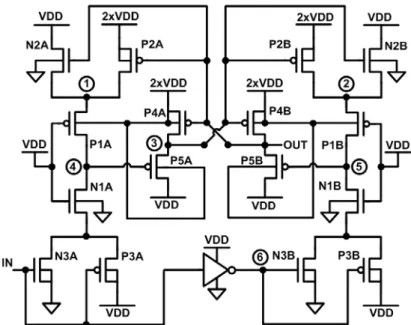
3.2.4 Level Converter
The level converter used in Fig. 3.3 and Fig. 3.4 are the same architecture, which can convert the voltage swing 0V-to-VDD to VDD-to-2xVDD [14]. As shown in Fig. 3.5, the level converter has been modified in this work with increasing the devices, N2A and N2B. Because when the devices, P2A and P2B, are turned off, the node 1
16
and node 2 are floating at this moment if there are no N2A and N2B in this structure. This is what we do not want to see in an integrated circuit. The increased n-channel transistors, N2A and N2B, can provide certain voltages (VDD) to node 1 and node 2 when the P2A and P2B are off. Therefore, the increased devices, N2A and N2B can guarantee the transistors related to node 1 and node 2 in a safe state. In Fig. 3.5, the bulks of the p-channel transistors which are related to the 2xVDD signals are connected to 2xVDD to avoid the leakage current producing by the conduction of the parasitic drain-to-well pn-junction diode. The voltage swing of input signals IN is from 0V to VDD. When signal IN is VDD, node 4 is pulled down to 0V, and transistor P5A is turned on. After transistor P5A is turned on, node 3 will be pulled down to VDD, and then P4B and P2B are turned on. Consequently, node OUT and node 5 are 2xVDD. At the same time, node 1 is pulled down to VDD because P2A is off and N2A is on, and then, transistor P1A is turned off.
Since the structure of the level converter is symmetrical, when signal IN is 0V, node 6 will be pulled high to VDD, and the operation is similar to the above. Finally, node OUT will be VDD and node 3 will be 2xVDD.
Fig. 3.5 The modified level converter which represents the level converter shown in Fig. 3.3 and Fig. 3.4.
17
3.2.5 Discussions
In some condition, the drain-to-bulk voltages of transistors MP, MN, and MPN are 2xVDD, but in general, the drain-to-bulk breakdown voltage is at least twice of the normal operating voltage in the standard CMOS process [15], [16]. Hence, the drain-to-bulk breakdown issue would be ignored in the proposed 2xVDD-tolerant I/O buffer. However, the reverse voltage of 2xVDD across the p-n junction results in larger leakage current in the substrate, it increases the power consumption and the potential that the circuit goes into latch-up. The designer should check the process parameters to make sure that the resulted leakage in the corresponding process is in an acceptable value. To decrease the leakage current, in the circuit’s layout, the distance between PMOS and NMOS should be kept longer to increase the equivalent resistance between the p-n junction of the bulks. Moreover, the transistors can be surrounded the guard ring to absorb the leakage currents.
In this new 2xVDD-tolerant I/O buffer, the bulk of MPN can be set at 0V without gate-oxide reliability problem, even if the gate voltage of MPN may be as high as 2xVDD. The reason is that this NMOS MPN is turned on if its gate voltage is 2xVDD, so the voltage across the gate oxide of MPN is from the gate to conducting channel but not from the gate to its bulk. The gate oxides of all NMOS devices in the new 2xVDD-tolerant I/O buffer are also safe because they are turned on when their gate terminals are pulled to 2xVDD.
3.3 Simulation Results
3.3.1 Function of Proposed 2xVDD-Tolerant I/O Buffer
It has been verified by simulation in a 0.18-µm CMOS process that the maximum voltage across any two terminals (gate, drain, and source) of each transistor in the proposed 2xVDD-tolerant output buffer is kept within VDD. The simulated
18
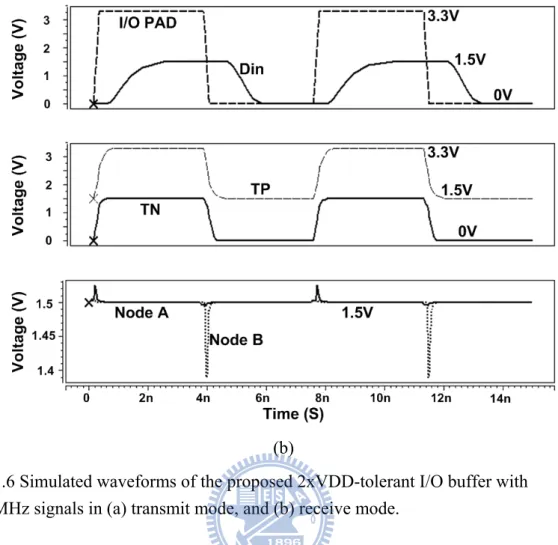
waveforms of the proposed I/O buffer to transmit or to receive 133-MHz 2xVDD signals with 10-pF loading and VDD of 1.5V are shown in Fig. 3.6.
As shown in Fig. 3.6 (a), when the I/O buffer is operating in the transmit mode, the nodes TP and TN are 1.5V. If it transmits 3.3-V signals, node A will be 3.3V and node B will be 1.5V. If it transmits 0-V signals, node A will be 1.5V and node B will be 0V. On the other hand, as shown in Fig. 3.6 (b), when the I/O buffer is operating in the receive mode, the nodes A and B are 1.5V. If it receives 3.3-V signals, node TP will be 3.3V and node TN will be 1.5V. If it receives 0-V signals, node TP will be 1.5V and node TN will be 0V.The simulated results are all consistent to this design expectation. The voltage across any two terminals of each transistor in the output stage would not exceed VDD.
19
(b)
Fig. 3.6 Simulated waveforms of the proposed 2xVDD-tolerant I/O buffer with 133-MHz signals in (a) transmit mode, and (b) receive mode.
The simulated power consumption is 24.3 mW in transmit mode to drive the 10-pF output loading at the frequency of 133 MHz. And the power consuming on the output loading dominates the total power consumption.
3.3.2 Slew Rate Effects of Input Signal in Receive Mode
The relation between the slew rate of the input signal and the leakage current of MP and MN in receive mode are shown in Fig.3.7. The input rise time/fall time is 0.2-ns in Fig. 3.7 (a) and 1-ns in Fig. 3.7 (b). The peak leakage currents of MP and MN in Fig. 3.7 (a) are larger than Fig. 3.7 (b). And the power consumption is 141 μW in Fig. 3.7 (a) and 113 μW in Fig. 3.7 (b). So, if the slew rate of the input signal is smaller, the leakage currents of MP and MN will be less.
20
(a)
(b)
Fig. 3.7 The simulation results of the current waveforms for MP and MN in the receive mode with the (a) 0.2-ns input rise time/fall time and (b) 1-ns input rise time/fall time.
21
The relationship between the slew rate of the input signal and the peak values of the gate-to-source and gate-to-drain voltage waveforms for MN and MP in receive mode are shown in Fig. 3.8. In the transient state, the gate-to-drain voltage would exceed 1.8V slightly for a short period of time. Comparing Fig. 3.8 (a) and Fig. 3.8 (b), it can be discovered that the peak values of the gate-to-drain voltage with 0.2-ns input rise time/fall time is larger than with the 1-ns input rise time/fall time. So, if the slew rate of the input signal is smaller, the performance of reliability will be better. Besides, the gate-to-source voltages in Fig. 3.8 (a) and Fig. 3.8 (b) are all still kept in 1.8V, so there is no reliability issue upon the gate-to-source voltages of MP and MN in receive mode.
22
(b)
Fig. 3.8 The simulation results of the gate-to-source and gate-to-drain voltage waveforms for MP and MN in the receive mode with (a) 0.2-ns input rise time/fall time and (b) 1-ns input rise time/fall time.
3.3.3 Discussion of Propagation Delay with Gate-Controlled Circuit
TABLE 3.2 discusses the leakage currents of MP and MN due to the propagation delays from I/O PAD to TP and from I/O PAD to TN. The propagation delays from I/O PAD to TP and from I/O PAD to TN dominate the turned-on time of MP and MN in the transient. Increasing the driving capability of MG3 and MG6 could make the MP and MN to be turned off more quickly. From TABLE 3.2, it can be discovered that power consumption is less than the original after increasing the size of MG3 and MG6.
23
Table 3.2
The relation between the propagation delay and the power consumption.
3.4 Experimental Results
3.4.1 Measurement Settings
The layout and die photo of the proposed 2xVDD-tolerant I/O buffer fabricated in a 0.18-μm 1.8-V CMOS process is shown in Fig. 3.9. The active area of the proposed I/O buffer is around 127μm x 785μm. The output stage dominates the major area of this I/O buffer. The area occupied by the control circuitry is about 15% of the I/O cell area. The printed circuit board (PCB) of tested 2xVDD-tolerant I/O buffer is shown in Fig. 3.10 and the measurement settings are shown in Fig. 3.11. As shown in Fig. 3.11 (a), when the 2xVDD-tolerant I/O buffer is operated in transmit mode, the signals at Dout generated by a pulse generator are transmitted to I/O PAD, and can be observed by a digital phosphor oscilloscope. In Fig. 3.11 (b), the signals are received at I/O PAD, and can be observed at Din by voltage probe when the 2xVDD-tolerant I/O buffer is operated in receive mode.
24
Fig. 3.9 The layout and die photo of the proposed 2xVDD-tolerant I/O buffer.
25
(a)
(b)
Fig. 3.11The measurement settings of the proposed 2xVDD-tolerant I/O buffer in (a) transmit mode and (b) receive mode.
26
3.4.2 Measurement Results
The measured waveforms of the proposed I/O buffer to transmit and receive 3.3-V signals are shown in Fig. 3.12 and Fig. 3.13 with VDD of 1.5V. Fig. 3.12 (a) and Fig. 3.12 (b) show the measured waveforms in transmit mode with respect to 1-MHz and 133-MHz I/O signals. It is noticed that the input Dout is 1.5V and the output voltage at the I/O PAD is 3.3V. Fig. 13 (a) and Fig. 13 (b) show the measured waveforms in receive mode with respect to 1-MHz and 133-MHz I/O signals, where the input voltage at the I/O PAD is 3.3V and the output Din is 1.5V. Due to the limitation of our pulse generator (HP 81110A), the output signal of this instrument operating in 133MHz is not a perfect pulse but a sinusoidal function with 3.3-V amplitude. Moreover, the threshold voltage of MI1 shown in Fig. 3.3 is about 0.5 V, so the input signal which is larger than 0.5 V will be considered as high signal. This results in the duty cycle being larger than 50%. The duty cycle can be well adjusted by additional duty-cycle adjustment circuit. The experimental results have confirmed that the proposed 2xVDD-tolerant I/O buffer can successfully transmit and receive 2xVDD signals up to 133MHz. The major speed limitation of this buffer is the driving capability of the output stage. It can be operated at a higher frequency if the transistor size of the output stage is increased.
The 2xVDD-tolerant I/O buffer has been successfully designed with dynamic source output technique and realized with 1xVDD CMOS devices in this thesis, which has been fabricated in a 0.18-μm 1.8-V CMOS process to transmit and receive 3.3-V signals without suffering gate-oxide reliability issue. The new proposed 2xVDD-tolerant I/O circuit solution can be implemented in different nanoscale CMOS processes to meet the mixed-voltage applications in microelectronic systems.
27
(a)
(b)
Fig. 3.12 The measured waveforms of the proposed I/O buffer in transmit mode with respect to (a) 1-MHz and (b) 133-MHz I/O signals.
28
(a)
(b)
Fig. 3.13 The measured waveforms of the proposed I/O buffer in receive mode with respect to (a) 1-MHz and (b) 133-MHz I/O signals.
29
Chapter 4
New 2xVDD-Tolerant I/O Buffer with
Slew-Rate Control
4.1
Introduction
Signal and power integrity are crucial problems in VLSI systems. Modern trends in deep sub-micron circuit designs, such as high operating frequencies, short rise/fall times, and lower supply voltage, exacerbate this problem. The pads of an output buffer on the PCB typically connect to series parasitic inductances produced by the bonding wire. An inductive noise will be induced in this condition. Ground Bounce, also known as simultaneous switching noise (SSN) or delta-I noise, is a voltage glitch induced at power/ground (P/G) distribution connections due to switching currents passing through either wire inductance or package lead inductance associated with power or ground rails. When the current flows through the inductance L, the voltage drop can be expressed as
di
V
L
dt
=
(4-1)The resulting noise voltage can potentially cause spurious transitions at the inputs of devices sharing the same power and ground rails. Therefore, controlling the output voltage variations is generally required to limit the crosstalk and reduce the inductive power supply noise to an acceptable value.
In this chapter, the new 2xVDD-tolerant I/O buffer proposed in chapter 3 is redesigned with slew-rate control to decrease the ground bounce effects.
30
4.2
Traditional Output Buffer with Slew-Rate Control
To reduce the simultaneous switching noise, a simple approach is to slow down the turn-on time of the output switching transistor through an access resister which can be implemented by a transmission gate to the transistor gate. Furthermore, the output driver can be divided into several output drivers and be turned on gradually for ground bounce reduction and slew-rate control. An output buffer with a three-step slew-rate control circuit is shown in Fig. 4.1 [17]. The output transistors are divided into three parts with their corresponding gate-controlled signals generated by slew-rate control circuit. The transistors MNS4 and MPS4 in Fig. 4.2 are used to control CMOS output driver to turn it on. When the output buffer is operating in transmit mode (OE=VDD), the transmission gates S1-S4 are used as resistive elements to turn on each individual output transistor gradually. As the output buffer is operating in tri-state mode, the output transistors are quickly turned off by the transistors MPS1-MPS3 and MNS1-MNS3 since the gate-controlled signals won’t pass through the transmission gates. With such structure of slew-rate control, the short- circuit current can be reduced efficiently for low power design.
The number of parts of an output buffer with slew-rate control can be extended to 4 bits or more. If the output buffer is divided into more parts, the switching current of each part in the output buffer can be decreased, but the propagation delay will be increased and the cost of the circuit is also increased. The designer should adjust the size of transmission gates and the size of each output driver to match the design requirements of the timing and noise specifications.
31
Fig 4.1 Conventional output buffer with slew-rate control.
4.3
New 2xVDD-Tolerant I/O Buffer with Slew-Rate Control
4.3.1 Circuit Implementation
In section 3.2, a new 2xVDD-tolerant I/O buffer to transmit and receive 2xVDD signals has been proposed. To reduce the effect of ground bounce, the new 2xVDD-tolerant I/O buffer is combined with a three-step slew-rate control circuit as shown in Fig. 4.2. Note that the total sizes of the output transistors in Fig. 4.2 are kept the same with output transistors in Fig. 3.3 for equal driving capacity. The voltage swing of MNS4, S1-S2 and MPS1-MPS3 are from VDD to 2xVDD for correct operating without gate-oxide overstress issue. The sizes of transmission gates affect the timing performance of the buffer. The small size can prolong the turn-on time of
32
the output switching transistor to minimize the ground bounce effect, but it also increases the delay time of circuit. The user can optimize the sizes of these transmission gates to match the specification. Because the switching current of the output transistors will result in the ground bounce, a major consideration is to reduce the peak switching current efficiently. A direct method is to let the size of output transistor which is turned on earlier be the smaller one. Because the drain-to-source voltage of the output transistor which is turned on later will be smaller than the earlier one, the equal size will make them have different driving capacity. So in Fig. 4.2, the size arrangements of these output transistors are MPP1 < MPP2 < MPP3 and MNN1 < MNN2 < MNN3. The corresponding size ratios are shown in Table 4.1.
33
Table 4.1
The size ratio of the output transistors
4.3.2 Simulation Results
The new 2xVDD-tolerant I/O buffer with slew-rate control has been verified in a 0.18-μm CMOS process by SPICE simulation with VDD of 1.5V and VDDH of 3.3V. The simulation waveforms with an operating speed of 133 MHz in transmit mode are shown in Fig 4.3. The gate-controlled signals MPP1-MPP3, VP1, VP2 and VP3, are pulled to 1.5V one by one as the 2xVDD-tolerant I/O buffer transmits 3.3-V output signal to I/O PAD. On the contrary, when 0-V output signal is transmitted to I/O PAD, the VP1, VP2 and VP3 are quickly pulled up to 3.3V to turn off transistors MPP1-MPP3. Similarly, the gate-controlled signals MNN1-MNN3, VN1, VN2 and VN3, are progressively pulled up to 1.5V in transmitting 0-V output signal and quickly pulled down to 0V to turn off transistors MNN1-MNN3 in transmitting 3.3-V output signal.
Table 4.2 summarizes the simulation results of the new 2xVDD-tolerant I/O buffer with or without slew-rate control. As a result, the switching currents of 2xVDD-tolerant I/O buffer with slew-rate control are smaller than those without slew-rate control. The timing specifications of 2xVDD-tolerant I/O buffer with slew-rate control are larger than those without slew-rate control. As shown in Table 4.2, the power consumption of new 2xVDD-tolerant I/O buffer with slew-rate control is a little less than those without slew-rate control due to the peak switching current reduction.
34
Fig 4.3 Simulation waveforms of the new 2xVDD-tolerant I/O buffer with slew-rate control operating at 133 MHz when transmitting 0V-to-1.5V output signals to I/O PAD.
Table 4.2
The simulation results of new 2xVDD-tolerant I/O buffer with or without slew-rate control.
35
4.3.3 Ground Bounce
In order to verify the reduction of ground bounce by slew-rate control, a model for ground bounce effects is shown in Fig. 4.4. The inductance of wire bonds vary from 7nH to 15nH in the simulation for typical cases. Since the switching currents of 2xVDD-tolerant I/O buffer in transmit mode are much larger than that in receive mode, the ground bounce effects are simulated in transmit mode for clear illustration. The simulation waveforms of ground bounce effects on power lines are shown in Fig. 4.5 and several parameters are defined as follows:
VDDH_ext / VDD_ext / VSS_ext : external power supply; VDDH_max : maximum value of VDDH power line; VSS_max : maximum value of VSS power line; VDDH_min : minimum value of VDDH power line; VSS_max : minimum value of VSS power line;
VDDH_over : overshot on VDDH power line (VDDH_max- VDDH_ext) VDDH_under : undershot on VDDH power line (VDDH_ext- VDDH_min) VSS_over : overshot on VSS power line (VSS_max- VSS_ext)
VSS_under : undershot on VSS power line (VSS_ext- VSS_min)
The VDDH_under and VSS_over among these parameters are the major concerns since these two terms may result in increasing timing delay and even logic errors on transmitted signals.
The simulation waveforms of the new 2xVDD-tolerant I/O buffer with slew-rate control which is operated in transmit mode with an operating speed of 133MHz are shown in Fig 4.6. The signals on I/O PAD are like sine wave with distortion due to the ground bounce effect. The simulation results with variation wire bond inductance on VDDH power line and VSS power line are shown in Fig. 4.7 and Fig. 4.8, respectively. Since the current supplied from VDD is much smaller than that from
36
VDDH, only ground bounce effect in VDDH is shown. As shown in Fig. 4.7 and Fig. 4.8, the slew-rate control circuit improves the ground bounce effects greatly.
I/O
Circuit
LVDDH LVDD LVSS VSS VDD VDDH VDDH_ext VDD_ext Input Output VSS_ext37
(a)
(b)
Fig 4.5 Simulation waveforms of ground bounce effects on (a) VDDH power line and (b) VSS power line.
Fig 4.6 Simulation waveforms of the 2xVDD-tolerant I/O buffer with slew-rate control for ground bounce effect in transmit mode.
38 6 8 10 12 14 16 0.2 0.4
Vol
tage (V)
Inductance (nH)
Without SR Control
With SR Control
(a) 6 8 10 12 14 16 0.4 0.6 0.8 1.0 1.2V
o
lt
ag
e (V
)
Inductance (nH)
Without SR Control
With SR Control
(b)Fig 4.7 The relation between ground bounce on VDDH power line and wire bond inductance on the new 2xVDD-tolerant I/O buffer with or without slew-rate control. (a) The overshoot and (b) the undershoot on VDDH power line.
39 6 8 10 12 14 16 0.2 0.4 0.6
V
o
lt
ag
e (V
)
Inductance (nH)
Without SR Control
With SR Control
(b) 6 8 10 12 14 16 0.4 0.6 0.8V
o
lt
ag
e (V
)
Inductance (nH)
Without SR Control
With SR Control
(b)Fig 4.8 The relation between ground bounce on VSS power line and wire bond inductance on the new 2xVDD-tolerant I/O buffer with or without slew-rate control. (a) The overshoot and (b) the undershoot on VSS power line.
40
Chapter 5
New 2xVDD-Tolerant I/O Buffer with
PVT Compensation
5.1
Introduction
In chapter 4, the new 2xVDD-tolerant I/O buffer with slew-rate control for ground bounce reduction has been discussed. Furthermore, to resist the slew-rate variation, the new 2xVDD-tolerant I/O buffer with PVT compensation will be illustrated in this chapter.
With the recent trend for high-speed interface, the sensitivity of circuits towards process, voltage and temperature (PVT) variation is hampering circuit performance and yield. For example, in the case of I/O pads it is difficult to meet the rise and fall times, current, power and ground bounce specifications across all PVT corners. Driver circuits are oversized to meet timing at slow corners. This causes high current and Simultaneous Switching Noise (SSN) at fast corners. Such effects degrade the reliability of the circuit and require considerable amount of design resources and time to meet circuit performance across PVT variation [18]. Therefore, recent interface specifications like UDMA 100 [19] are not only to limit the minimum or maximum value the timing specification but also require the slew rate keeping in a certain range. In next section, a method of PVT compensation to make the output slew rate be kept as constant as possible will be illustrated.
41
5.2
New 2xVDD-Tolerant I/O Buffer with PVT Compensation
Fig. 5.1 shows the design concept of the PVT compensation technique to keep the output slew rate of an I/O buffer within in a certain range [20]. As shown in Fig. 5.1, the PVT variation detector detects process, voltage, and temperature variations by sensing the reference clock in different conditions. Then the PVT variation detector will generate the corresponding pre-control signals to the encoder. The encoder using these pre-control signals to generate applicable control signals to the output stage of an I/O buffer. The drive strength of the output driver can be adjusted with these control signals to match the PVT variation. The detail implementation will be illustrated as following.
Fig 5.1 Block diagram of solution for PVT compensation.
5.2.1 PVT Variation Detector
The schematic of the PVT variation detector is shown in Fig. 5.2. First, the reference clock delivers the logic high into the delay chain. Then once the reference clock turns to logic low, the outputs of each delay cells will be load into the register. Because the propagation delay of a delay cell depends on the process, voltage and temperature, the propagation delay determines how many the signals of logic high
42
will be load into the register. For example, in the fast condition, the signal of logic high can pass through many delay cells in a reference clock cycle. On the contrast, in the slow condition, most of the delay cells’ outputs will be logic low since the signal logic high has not been delivered to them when the reference clock turns to logic low. As shown in Fig. 5.3, the register in Fig. 5.2 is implemented with the pulse triggered D flip-flop. Thus, the register loads data in the moment that the reference clock turns to logic low. Next the outputs of this register will be converted to the pre-control signals by several logic gates for convenient application in the output stage. For the new 2xVDD-tolerant I/O buffer with PVT compensation, the 2xVDD power supply variation should be sensed in the PVT variation detector. Therefore, the logic gates should be implemented with the 2xVDD-tolerant logic gates which will be illustrated in section 5.3.
43
Fig 5.3 The pulse triggered D flip-flop using as the register in the PVT variation detector.
5.2.2 Encoder
In order to control the segmented output driver which will be illustrated in next section conveniently, the pre-control signals from the PVT variation detector have to be encoded appropriately. Table 5.1 shows the truth table of encoder in the PVT compensation circuit. The D0-D7 are the pre-control signals from the PVT variation detector. All the situations that D0-D7 could be are listed in the truth table. In the fastest condition, the signals of D0-D7 are “00000001”. On the contrast, the signals of D0-D7 are “10000000” in the slowest condition. The pre-signals D0-D7 are encoded to the binary codes S0-S2. If signals of S0-S2 are logic high, it means that the corresponding segmented output driver is turned on. The implementation of this 8-to-3 encoder is shown in Fig. 5.4. Since the circuit is implemented with the 2xVDD-tolerant logic gates whose voltage swing is from 0V to 2xVDD, the outputs S0-S2 should be converted to S0H-S2H and S0L-S2L by the level converter for being
used correctly in the output stage. The voltage swing of S0H-S2H is from VDD to
2xVDD and voltage swing of S0L-S2L is from 0V to VDD. As shown in Fig. 5.4, the
level converter converts 0V-to-2xVDD signals to VDD-to-2xVDD and 0V-to-VDD signals. The detail implementation of this level converter will be illustrated in section 5.3.
44
Table 5.1
Truth table of Encoder in the PVT compensation circuit.
45
5.2.3 Output Stage with Control Signals
The schematic of new 2xVDD-tolerant I/O buffer with PVT compensation is shown in Fig. 5.5. S0H-S2H and S0L-S2L are the PVT variation related signals which
are generated from the PVT variation detector and the encoder. With the OR gates and AND gates shown in Fig. 5.5, the S0H-S2H and S0L-S2L can be used to determined the
segmented output drivers to be turn on or turn off. Because the voltage swing of S0H-S2H is from VDD to 2xVDD, the voltage swing of OR gates is from VDD to
2xVDD. Similarly, because the voltage swing of S0L-S2L is from 0V to VDD, the
voltage swing of AND gates is from 0V to VDD. Since S0H-S2H and S0L-S2L are
binary codes and their weighting are S2H > S1H > S0H and S2L > S1L > S0L, the size
weightings of these segmented output drivers are MPP2 > MPP1 > MPP0 and MNN2 > MNN1 > MNN0. The output transistors MPP and MNN are the basic output driver, so when the binary codes are “000” which happens in the slowest condition, only MPP and MNN will be used. Therefore, the size of MPP and MNN can be determined to match the driving capacity of typical condition in slowest condition. Next, the size of MPP1 and MNN1 can be determined to match the driving capacity of typical condition in the condition whose corresponding codes are “001”, because only MPP, MNN, MPP1 and MNN1 are used in this condition. Following such design strategy, the sizes of all the output drivers can be roughly determined. Note that the driving capacity is precise in the design point like “000” and “001” with such design strategy, but it will be a little oversized or undersized in other conditions like “011” or “101”. However, the design strategy provides a way to grasp approximate trend of the size change of the output driver. The corresponding size ratios of the output drivers are shown in Table 5.2. Furthermore, the bits of the control signals can be extended to 4 bits or more. The 4-bit control signals example of the 2xVDD-tolerant I/O buffer with PVT compensation is shown in Fig. 5.6.
46
Fig 5.5 The schematic of new 2xVDD-tolerant I/O buffer with PVT compensation.
Table 5.2
47
Fig 5.6 The schematic of new 2xVDD-tolerant I/O buffer with PVT compensation of 4-bit control signals.
5.3
Proposed 2xVDD-Tolerant Logic gate
In order to detect the 2xVDD power supply variation, the delay chain should be implemented with the 2xVDD-tolerant logic gates. For consistency, all the logic gates in the PVT variation detector are the structure of 2xVDD-tolerant logic gates. Of course, the voltage level of 2xVDD can be also shifted to VDD by a level converter and be dealt with normal logic gates. This paper just proposed a direct way by using the 2xVDD-tolerant logic gates to accomplish this work.
The voltage swing of inputs and outputs of the 2xVDD-tolerant logic gates are from 0V to 2xVDD. Fig. 5.7 shows the schematic of 2xVDD-tolerant inverter. As shown in Fig. 5.7, the signal IN whose voltage swing is from 0 to 2xVDD is converted to INH and INL. The voltage swing of INH is from VDD to 2xVDD and the
48
voltage swing of INL is from 0V to VDD. The output stage in the 2xVDD-tolerant
inverter is the dynamic source structure which is proposed in chapter 3. MP and MN are the stacked structure to prevent the 2xVDD-tolerant inverter suffering gate-oxide overstress. MPP and MNN decide the function of this logic. MPN and MNP are used to bias node A and node B at safe voltage when MPP and MNN are turned off.
Fig 5.7 The 2xVDD-tolerant inverter.
The level converter shown in Fig. 5.8 is used to convert the voltage swing of 0V-to-2xVDD into VDD-to-2xVDD and 0V-to-VDD. As shown in Fig. 5.8, when the IN is 2xVDD, the MP1 is turned on while the MP2 is turned off, so the INH will be
2xVDD. On the other hand, the MN2 is turned on while MN1 is turned off, so the INL
will be VDD. When the IN is 0V, the MP2 is turned on while the MP1 is turned off, so the INH will be VDD. On the other hand, the MN1 is turned on while MN2 is turned
off, so the INL will be 0V. Using such level converter can correctly control the
49
Fig 5.8 The level converter being used in the 2xVDD-tolerant I/O logic gates and the encoder circuit which is shown in Fig. 5.4.
Fig. 5.9 shows the examples of 2-input 2xVDD-tolerant NAND gate and 2-input 2xVDD-tolerant NOR gate. As shown in Fig. 5.9 (a), the input A is converted to AH
and AL, and input B is converted to BH and BL by the level converter shown in Fig. 5.8.
Fig. 5.9 (b) shows the example of 2-input 2xVDD-tolerant NAND gate. MP and MN are the stacked structure to prevent the 2xVDD-tolerant inverter suffering gate-oxide overstress. MPP1 MPP2, MNN1 and MNN2 decide the function of this logic. MPN1 MPN2, MNP1 and MNP2 are used to bias node A and node B at safe voltage when node A and node B are floating. Note that if the function transistors (MNN1 and MNN2) are series structure, the biasing transistors (MNP1 and MNP2) will be the parallel structure. They are complementary structure. As well as if the function transistors (MPP1 and MPP2) are parallel structure, the biasing transistors (MPN1 and MPN2) will be the series structure. Fig. 5.9 (c) shows the example of 2-input 2xVDD-tolerant NOR gate. Similarly, MP and MN are the stacked structure to
50
prevent the 2xVDD-tolerant inverter suffering gate-oxide overstress. MPP1 MPP2, MNN1 and MNN2 decide the function of this logic. MPN1 MPN2, MNP1 and MNP2 are used to bias node A and node B at safe voltage when node A and node B are floating. Again, their function transistors and biasing transistors are the complementary structure. Basing on this design method, all the 2xVDD-tolerant logic gates can be implemented even the inputs are more than two. The implementations of the 3-input 2xVDD-tolerant NAND gate and NOR gate are shown in Fig. 5.10. As shown in Fig. 5.10 (a), there needs three level converters to convert the inputs A, B, and C. Fig. 5.10 (b) shows the example of 3-input 2xVDD-tolerant NAND gate and Fig. 5.10 (c) shows the example of 3-input 2xVDD-tolerant NOR gate. Using these 2xVDD-tolerant logic gates in the PVT compensation circuit can detect the variation of 2xVDD power line in a mixed-voltage I/O circuit.
51
(b) (c)
Fig 5.9 The implementations of 2-input 2xVDD-tolerant logic gates. (a) The inputs (b) NAND gate, and (c) NOR gate.
52
(b) (c)
Fig 5.10 The implementations of 3-input 2xVDD-tolerant logic gates. (a) The inputs (b) NAND gate, and (c) NOR gate.
5.4
Simulation Results
The new 2xVDD-tolerant I/O buffer with PVT compensation has been verified in a 0.18μm CMOS process by SPICE simulation. In section 5.4.1, the slew rate variation will be compared with or without PVT compensation using 3-bits control signals. Furthermore, the control bits will be extended to 4 bits in order to increase the precision. The corresponding simulation results about the 4-bits control signals will be discussed in section 5.4.2.
5.4.1 Simulation Results with 3-bits control signals
Table 5.4 shows the simulated slew rate of the I/O PAD of the new 2xVDD-tolerant I/O buffer without PVT compensation. The definition of slew rate is
![Fig. 2.1 Design concept for traditional mixed-voltage I/O buffer realized with only thin-oxide devices [4]](https://thumb-ap.123doks.com/thumbv2/9libinfo/8237721.171218/18.892.230.667.662.1065/design-concept-traditional-mixed-voltage-buffer-realized-devices.webp)
![Fig 2.2 shows the mixed-voltage I/O buffer with a blocking NMOS and a dynamic gate-bias circuit proposed in [7]](https://thumb-ap.123doks.com/thumbv2/9libinfo/8237721.171218/19.892.272.649.885.1153/shows-mixed-voltage-buffer-blocking-dynamic-circuit-proposed.webp)