IEEE ELECTRON DEVICE LETTERS, VOL. 25, NO. 6, JUNE 2004 393
Hot-Carrier Effects on Power Characteristics
of SiGe HBTs
Sheng-Yi Huang, Kun-Ming Chen, Member, IEEE, Guo-Wei Huang, Member, IEEE, Hua-Chou Tseng, Tsun-Lai Hsu,
Chun-Yen Chang, Fellow, IEEE, and Tiao-Yuan Huang, Fellow, IEEE
Abstract—This letter investigates hot-carrier (HC) effects
on the power characteristics of Si–SiGe HBTs using load-pull measurements. We found that the output power, power gain, and linearity of Si–SiGe HBTs are degraded after HC stress. Under constant base-current measurement, the HC-induced power performance degradation is found to be much worse than that under constant collector-current measurement. The HC effects on the cutoff frequency, nonlinearity terms of base-current and collector-current, and third-order intermodulation (IM3) cancellation effect have been analyzed to explain the experimental observations.
Index Terms—Hot-carrier (HC) stress, linearity, load-pull
mea-surement, power, SiGe HBT.
I. INTRODUCTION
W
ITH RECENT technology advancements that push cutoff frequency and maximum oscillation frequency over 200 GHz [1], [2], SiGe HBTs have become viable candidates for most microwave applications. Recently, SiGe HBTs have attracted much attention for RF power application because of their excellent microwave power performance and high thermal conductivity [3], [4]. Due to the high electric field at the base–emitter junction caused by the high doping levels of SiGe HBTs, the hot-carrier (HC) reliability has become a major concern for advanced devices used in commercial products [5]. However, the majority of literatures on HC effects deals mainly with the dc characteristics and/or the low-frequency noise behavior [6]–[8], and seldom addresses the RF characteristics [9], [10]. In this letter, we investigate HC effects on the output power, power gain and the linearity of the SiGe HBTs for the first time. For load-pull measurements, the operating frequency was chosen at 2.4 GHz, a frequency commonly used in wireless communication.II. EXPERIMENTS
Multifinger SiGe HBTs were fabricated with a typical 0.24 m high-voltage SiGe HBT process. The nominal emitter width of the four-finger-stripe device is 1 m, and the length
Manuscript received December 17, 2003; revised March 15, 2004. This work was supported in part by Semiconductor Research Corporation under Contract 2003-MJ-1089. The review of this letter was arranged by Editor E. Sangiorgi.
S.-Y. Huang, C.-Y. Chang, and T.-Y. Huang are with the Department of Elec-tronics Engineering and the Institute of ElecElec-tronics, National Chiao Tung Uni-versity, Hsinchu 300, Taiwan, R.O.C.
K.-M. Chen and G.-W. Huang are with the National Nano Device Laborato-ries, Hsinchu 300, Taiwan, R.O.C.
H.-C. Tseng and T.-L. Hsu are with the United Microelectronics Corporation, Hsinchu 300, Taiwan, R.O.C.
Digital Object Identifier 10.1109/LED.2004.828589
Fig. 1. Gummel plot of a typical SiGe transistor before and after stress. For power characterization, the collector-currentI and base-current I are 52 and 0.34 mA, respectively, before stress. After stress,I changes to 0.7 mA under constant collector-current measurement, whileI changes to 24 mA for constant base-current measurement. Inset shows the reverse base–emitter junction characteristics before and after stress with collector open.
is 32 m. The devices exhibit a dc current gain of up to 181 and the BV is 5.3 V. Typical cutoff frequency and maximum oscillation frequency are about 23 and 40 GHz, respectively. The HC stress was carried out by applying a reverse-biased base–emitter voltage of 3.5 V up to 1000 seconds at room temperature, and with the collector left open. The applied is near to the base–emitter junction breakdown voltage (see inset of Fig. 1) in order to enhance the hot carrier effect. The output power, power gain, and linearity were measured using the load-pull system, which consisted of HP85122A and ATN LP1 (power parameter extraction soft-ware). The source and load impedance was tuned for maximum power gain and maximum output power, respectively. All the experiments were carried out at the wafer level on a set of five samples.
III. RESULTS ANDDISCUSSION
The Gummel plot of a typical SiGe transistor measured be-fore and after HC stress is shown in Fig. 1. It can be seen that the main effect of HC stress on the dc characteristics is an in-crease of the nonideal base-current. And the ideality factor of base-current will increase from 1 to about 1.5 at medium currents (see Table I). Since the collector-current remains es-sentially unchanged, the dc current gain decreases after HC stress. This degradation mode is similar to previous literature report, and is ascribed mainly to hot holes [6]. The hot holes
394 IEEE ELECTRON DEVICE LETTERS, VOL. 25, NO. 6, JUNE 2004
TABLE I
LINEARPOWERGAIN, OUTPUTPOWER AT1 dB GAINCOMPRESSIONPOINT,
IIP3ANDKEY DCPARAMETERS FOR ATYPICALSiGe TRANSISTOR
BEFORE ANDAFTERSTRESS. VV = 3 V
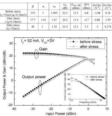
Fig. 2. Output power and power gain versus input power before and after stress measured at a fixed collector-current. Inset showsjh j versus frequency.
generate interface traps at Si–SiO interface of the base–emitter junction. Since the current gain is reduced after HC stress, the microwave and power characteristics of the transistor should be affected as well.
Fig. 2 shows the effects of HC stress on the output power and power gain of a transistor measured at a fixed collector-cur-rent of 52 mA. The optimized matched source and load imped-ances are essentially unchanged after HC stress. After HC stress, the output power and power gain decrease slightly in the small input power regime, but show no noticeable change in the high power regime. For class A operation, the linear power gain of amplifiers can be expressed as [11]
(1) where is the emitter resistance, is the base resistance, is the emitter lead inductance, is the base–emitter ca-pacitance, and is the operating frequency. The corresponding small-signal current gain versus frequency curve is plotted in the inset of Fig. 2. It can be seen that the magnitude of the small-signal current gain decreases after stress at low fre-quency regime, while remains essentially unchanged for
GHz. This result is similar to that of Si bipolar transistors re-ported in [12]. The decrease of at low frequency is consistent with the degradation of the dc current gain. At high frequency, the stress-induced traps cannot respond to the signal variation, so the magnitude of remains essentially unchanged [12]. This result explains why the cutoff frequency and the power gain, when measured at a constant collector-current, change only slightly after stress. After gain compression, because the
Fig. 3. Output power and power gain versus input power before and after stress measured at a fixed base-current. Inset showsjh j versus frequency.
collector-current is kept at a constant value, the output power and power gain even show no noticeable change under stress.
When the measurements were carried out by keeping a constant base-current, the output power and power gain show significant degradations after stress, as shown in Fig. 3. It is worth noting that the optimized matched conditions have been changed after stress due to the change of the collector-current. If we fixed the source and load impedances, the degradation of power performance after stress would be even worse, due to the mismatched condition. From the inset of Fig. 3, it can be seen that deviation occurs after stress over the entire frequency range. This is because the collector-current is reduced after stress. As a result, the emitter transit time which is inversely proportional to the collector-current increases and thus degrades the cutoff frequency, resulting in the degradation of output power and power gain. Since the collector-current is reduced after stress, it will limit the maximum magnitude of the output waveform to lower values, and thus the compression point will shift to lower output power. Hence, the degradation in power gain and output power will be more pronounced in the high power regime. Although the power gain is reduced after stress, the power-added efficiency changes only slightly (from 40% to 39%), due to the concomitant reduction of dc output power dissipation.
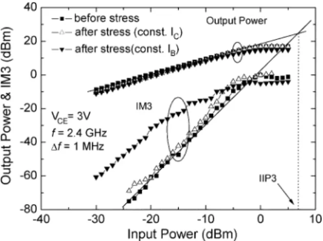
To study the HC stress effects on the linearity of a microwave system, the two-tone load-pull measurement was also carried out [13]. To characterize the linearity, the third-order intercept point, at which the output power and third-order intermodula-tion (IM3) are equal, is commonly used, as shown in Fig. 4. For low distortion operation, the third-order intercept point should be as high as possible. The values of input third-order inter-cept point (IIP3) before and after HC stress are summarized in Table I. While the before-stress value is about 6.8 dBm, the after-stress IIP3 reduces to 3.33 dBm and 2.46 dBm for con-stant collector-current and concon-stant base-current measurements, respectively.
The major nonlinear elements in a bipolar transistor are the collector-current , base-current , base–emitter charge , and base–collector charge [14]. Since the HC stress does not affect the base–collector junction, we only need to consider
HUANG et al.: HOT-CARRIER EFFECTS ON POWER CHARACTERISTICS OF SiGe HBTs 395
Fig. 4. Output power and third-order intermodulation power versus input power for a SiGe HBT before and after stress.
the distortion from the nonlinear exponential functions of , , and . These nonlinear sources can be expanded using Taylor series in the vicinity of its bias point yielding [14]
(2) where is the base–emitter voltage signal, and is the forward transit time. From the third-order derivative of the current versus , we can estimate the nonlinear effect of the current source itself. When measured at the same
collector-cur-rent, the data of and show only slight
deviation under stress (see Table I). However, the ideality factor of base-current has changed drastically from 1.005 to 1.52 after stress, indicating that partial IM3 cancellation, which has been attributed to the interaction of and , or and , has been reduced [14]. So the reduction of IIP3 after stress is mainly due to the reduced cancellation effect. However, with a constant base-current measurement, not only increases to 1.67 after stress, but and also depict large variation. Hence, the degradation of linearity measured at constant base-current is much worse than that measured at constant collector-current.
IV. CONCLUSION
In this letter, the effects of HC stress on power characteris-tics of Si–SiGe HBTs have been examined in detail. HC stress reduces the current gain and cutoff frequency, while degrades the ideality factor of the base-current. Consequently, the output power, power gain, and linearity of the transistor show signifi-cant performance degradation. We have compared stress effects at various bias conditions. It is observed that the performance degradation is much smaller under constant collector-current measurement, compared to constant base-current measurement.
It is therefore suggested that the Si–SiGe amplifier performance can be made more robust to HC effects by biasing the HBT at constant collector-current.
ACKNOWLEDGMENT
The authors would like to thank the staff of UMC for their helpful comments.
REFERENCES
[1] J.-R. Rieh, B. Jagannathan, H. Chen, K. T. Schonenberg, D. Angell, A. Chinthakindi, J. Florkey, F. Golan, D. Greengerg, S.-J. Jeng, M. Khater, F. Pagette, C. Schnabel, P. Smith, A. Stricker, K. Vaed, R. Volant, D. Ahlgren, G. Freenman, K. Stein, and S. Subbanna, “SiGe HBTs with cutoff frequency of 350 GHz,” in IEDM Tech. Dig., 2002, pp. 771–774. [2] B. Jagannathan, M. Khater, F. Pagette, J.-S. Rieh, D. Angell, H. Chen, J. Florkey, F. Golan, D. R. Greenberg, R. Groves, S. J. Jeng, J. Johnson, E. Mengistu, K. T. Schonenberg, C. M. Schnabel, P. Smith, A. Stricker, D. Ahlgren, G. Freeman, K. Stein, and S. Subbanna, “Self-aligned SiGe NPN transistors with 285 GHzf and 207 GHzf in a manufac-turable technology,” IEEE Electron Device Lett., vol. 23, pp. 258–260, May 2002.
[3] J. N. Burghartz, J.-O. Plouchart, K. A. Jenkins, C. S. Webster, and M. Soyuer, “SiGe power HBTs for low-voltage, high performance RF appli-cations,” IEEE Electron Device Lett., vol. 19, pp. 103–105, Apr. 1998. [4] M. Zhenqiang, S. Mohammadi, P. Bhattacharya, L. P. B. Katehi, S. A.
Alterovitz, and G. E. Ponchak, “A high-power and high-gain X-band Si–SiGe–Si heterojunction bipolar transistor,” IEEE Trans. Microwave
Theory Tech., vol. 50, pp. 1101–1108, Apr. 2002.
[5] L. Vendrame, P. Pavan, G. Corva, A. Nardi, A. Neviani, and E. Zanoni, “Degradation mechanism in polysilicon emitter bipolar junction transistors for digital application,” Microelectron. Reliab., vol. 40, pp. 207–230, 2000.
[6] A. Neugroschel, C. T. Sah, and M. S. Carroll, “Degradation of bipolar transistor current gain by hot holes during reverse emitter-base bias stress,” IEEE Trans. Electron Devices, vol. 43, pp. 1286–1290, Oct. 1996.
[7] U. Gogineni, J. D. Cressler, G. Niu, and D. L. Harame, “Hot electron and hot hole degradation of UHV/CVD SiGe HBTs,” IEEE Trans. Electron
Devices, vol. 47, pp. 1440–1448, July 2000.
[8] P. Llinares, S. Niel, G. Ghibaudo, L. Vendrame, and J. A. Chroboczek, “Retarding effect of surface base compensation on degradation of noise characteristics of BICMOS BJTs,” Microelectron. Reliab., vol. 37, pp. 1603–1606, 1997.
[9] M. Borgarino, J. G. Tartarin, J. Kuchenbecker, T. Parra, H. Lafontaine, T. Kovacic, R. Plana, and J. Graffeuil, “On the effects of hot carriers on the RF characteristics of Si–SiGe heterojunction bipolar transistor,”
IEEE Microwave Guided Wave Lett., vol. 10, pp. 466–468, Nov. 2000.
[10] J. Kuchenbecker, M. Borgarino, L. Bary, G. Cibiel, O. Llopis, J. G. Tar-tarin, J. Graffeuil, S. Kovacic, J. L. Roux, and R. Plana, “Reliability in-vestigation in SiGe HBTs,” Silicon Monolithic Integrated Circuits in RF
Systems, pp. 131–134, 2001.
[11] G. B. Gao, H. Morkoc, and M. C. Frank, “Heterojunction bipolar tran-sistor design for power applications,” IEEE Trans. Electron Devices, vol. 39, pp. 1987–1997, Sept. 1992.
[12] A. K. Kapoor, C. H. Lin, and S. Y. Oh, “Effect of emitter-base reverse bias stress on high frequency parameters of bipolar transistors,” in Proc.
IEEE IRPS, 1991, pp. 188–192.
[13] Y. Yang, J. Yi, J. Nam, B. Kim, and M. Park, “Measurement of two-tone transfer characteristics of high-power amplifiers,” IEEE
Trans. Microwave Theory Tech., vol. 49, pp. 568–571, Mar. 2001.
[14] M. Iwamoto, P. M. Asbeck, T. S. Low, C. P. Hutchinson, J. B. Scott, A. Cognata, Q. Xiaohui, L. H. Camnitz, and D. C. D’Avanzo, “Lin-earity characteristics of GaAs HBTs and the influence of collector de-sign,” IEEE Trans. Microwave Theory Tech., vol. 48, pp. 2377–2388, Dec. 2000.