國
立
交
通
大
學
材料科學與工程研究所
博 士 論 文
偏角度基板對穿隧層之效應與成長砷化鎵於鍺/矽基
板上對低成本高效率多接面三五族太陽電池之應用
Substrate Misorientation Effects in Tunnel Junction Layers and GaAs Epitaxy
Grown on Ge/Si Substrate for Low-cost High-efficiency III-V Multijunction
Solar Cell Applications
研 究 生:游 宏 偉
指導教授:張 翼 教授
偏角度基板對穿隧層之效應與成長砷化鎵於鍺/矽基
板上對低成本高效率多接面三五族太陽電池之應用
Substrate Misorientation Effects in Tunnel Junction Layers and GaAs Epitaxy
Grown on Ge/Si Substrate for Low-cost High-efficiency III-V Multijunction
Solar Cell Applications
研 究 生:游宏偉 Student:Hung-Wei Yu
指導教授:張 翼 Advisor:Edward Yi Chang
國 立 交 通 大 學
材料科學與工程研究所
博 士 論 文
A Thesis Submitted to Department of Materials Science and Engineering
National Chiao Tung University
in partial Fulfillment of the Requirements
for the Degree of Doctor of Philosophy in
Material Science and Engineering
June 2012
Hsinchu, Taiwan, Republic of China
-i-
偏角度基板對穿隧層之效應與成長砷化鎵於鍺/矽基板上對低
成本高效率多接面三五族太陽電池之應用
學生:游宏偉
指導教授:張 翼 博士
國立交通大學材料科學與工程研究所 博士班
摘
要
為了提升三五族太陽能電池在此領域之競爭力,首先必須要增加其光電轉換
效率並降低其發電成本。在此論文中,我們證明偏角度基板對三五族多接面太陽
能電池中砷化鋁鎵/砷化鎵穿隧層(AlGaAs/GaAs tunnel diodes, TDs)材料特性有一
定影響。當砷化鋁鎵/砷化鎵穿隧層成長於 10 度砷化鎵基板上時,此時穿隧層表
面粗糙度可降至 0.154nm 並產生最佳界面狀況。實驗結果也證實此基板可有效降
低砷化鎵層中氧等不純物濃度;也可減少砷化鋁鎵層中非等向性位置(anisotropic
sites),進而減少此層在成長過程中不純物含量以提升三五族太陽能電池光電轉換
效率。同時,我們也證實磷化銦鎵/砷化鎵(InGaP/GaAs)雙接面太陽電池中使用砷
化鋁鎵/砷化鎵穿隧層(成長於 10 度砷化鎵基板上)可得到較高光電轉換效率
(~20%)與外部量子效率(InGaP 子電池: 82% ; GaAs 子電池: 85%)。由高聚光測試
(~185×)結果發現,使用砷化鋁鎵/砷化鎵穿隧層之磷化銦鎵/砷化鎵雙接面太陽電
池之光電特性較使用磷化銦鎵/砷化鎵穿隧層之雙接面太陽電池來的高。此外,
如果能將砷化鎵等三五族材料成長於矽基板上取代傳統以鍺為基板的模式,將可
大大降低三五族太陽能電池發電成本。本研究發現將變溫砷界面層成長於經過
650 度熱退火之鍺/矽基板可有效改善隨後成長之砷化鎵層磊晶品質(表面粗糙
度:1.1nm;缺陷密度: ~2x10
7cm
-2)。本研究亦證實由於砷-鍺、鎵-鍺間鍵節能量之
不同與低砷流量之緣故,使砷化鎵/鍺/矽異質結構間之砷與鍺原子內部擴散可有
效被抑制。此實驗結果證明變溫砷界面層成長於鍺/矽基板上對未來欲成長三五
族微電子元件或光電元件於矽基板上將具有極大潛力。
-ii-
Substrate Misorientation Effects in Tunnel Junction Layers
and GaAs Epitaxy Grown on Ge/Si Substrate for Low-cost
High-efficiency III-V Multijunction Solar Cell Applications
student:Hung-Wei Yu
Advisors:Dr. Edward Yi Chang
Department of Materials Science and Engineering
National Chiao Tung University
ABSTRACT
To further promote the competitiveness of III-V multijunction solar cells in the
field, the conversion efficiency of solar cells has to increase while their cost must be
reduced. In this thesis, we have demonstrated that the material properties of the
P
++-AlGaAs/N
++-GaAs tunnel diodes (TDs) could be affected by misoriented GaAs
substrates for III-V multijunction solar cell applications. The best surface morphology
(0.154nm) and interface sharpness for the TDs were obtained on the (100) tilted 10°
off toward [111] GaAs substrate. TD materials grown on this substrate can efficiently
reduce oxygen-incorporation in N
++-GaAs layer, and also reduce the anisotropic sites
for oxygen-incorporation in the P
++-AlGaAs layers. We also proved that InGaP/GaAs
dual junction solar cells with a P
++-AlGaAs/N
++-GaAs TD grown on 10°off GaAs
substrates exhibit superior photovoltaic conversion efficiency (~20%) when operated
at one sun, and produces higher EQE (~82% for InGaP top cell and 85% for GaAs
bottom cell) as compared to the P
++-GaAs/N
++-InGaP TD. The cell design with a
P
++-AlGaAs/N
++-GaAs TD grown on 10°off GaAs substrates also displays superior
-iii-
I-V characteristics when these solar cell devices were operated at higher concentration
ratios (~185×). On the other hand, production cost of III-V multijunction solar cells
can be largely reduced while III-V materials, such as GaAs epitaxy, are grown on Si
substrates instead of traditional Ge substrates. We have demonstrated that the As
prelayer grown using graded-temperature technique on the Ge/Si substrate annealed at
650°C effectively improves the epitaxial quality of GaAs epitaxy (roughness: 1.1 nm,
dislocation density: ~2x10
7cm
-2). Furthermore, the interdiffusion of Ge and As atoms
in the GaAs/Ge/Si heterostructure can be effectively suppressed by the
graded-temperature As prelayer because of the difference in energies between As-Ge
and Ga-Ge bonds and low As flux. These results suggest that the graded-temperature
As prelayer grown on Ge/Si substrate has great potential for use in the growth of III-V
nanoelectronic devices and optoelectronic devices on the Si substrate.
-iv-
誌
謝
在這 4~5 年博士班生涯裡,首先要感謝我的指導老師張翼教授,他不僅提供
儀器設備讓我們做實驗並實現心中想法之外,也會在我們研究領域上提供創新的
見解,讓我們瞭解到只要肯努力、用心於研究上便有機會成功。除此之外,張翼
老師也會常常舉辦實驗室聚餐,讓大家在研究煩悶環境中獲得一絲舒緩,並與研
究室就其他成員有交流機會,在聚會當中時常獲得其他意見與想法,這些都有助
於解決實驗上所遇到之瓶頸。
在此我也要感謝我的研究夥伴 Quan,在創組之初我們一起修過 MOCVD 並一
同度過徬徨無助的時期,不過我們也在此過程中培養出患難與共的革命情感與絕
佳的默契,並祝福他在未來之路平安又順遂;感謝黃延儀博士,謝謝他在實驗過
程中提供我一些寶貴經驗與分析知識,使我對我實驗數據有更深一層了解,使我
有機會發到較好的國際期刊;感謝我的好友張榮庭,感謝他不吝提供我他十幾年
MO 經驗,使我短短三年獲得他多年功力,使我突飛猛進,在此祝福他家庭美滿、
和樂;還有我們 solar 組第一畢業碩班學弟王韋傑,感謝他在實驗上的協助並在
實驗經過無數次失敗後依然保有那熱忱的心,與我一起奮戰到最後進而攜手邁向
成功;還有我們 solar 組之花珍珍,要感謝她在百忙之中還幫我做製程,使我的
研究成果可以進一步得到證實,也常常在實驗失敗時扮演 “仙姑”角色,使我感
覺實驗失敗也是一種享受;感謝青翔學弟,謝謝你在實驗上提供一些想法,使我
思緒更寬廣;感謝 solar 組其他學弟們(道遠、尊民、Hoa、訓瑞)在口試上所提供
協助,使我口試得以順利進行,感謝你們。要感謝人太多,無法在此一一說明,
只好在此跟您說聲 “感謝”
最後感謝我的父母多年對我的支持與期待,沒有他們也不會有今天的我;也
要感謝我的女友慧玲,謝謝她多年來沒有給我一絲壓力,並常體諒我因實驗不順
遂所發的脾氣,還決心跟我一起走到永遠,我要告訴她: 謝謝,我愛妳。
v
Contents
Abstract (Chinese) ………... i Abstract (English) ……… ii Acknowledgement ………..…. iv Contents ………... vTable Captions ……..………. viii
Figure Captions …..….………...… ix
Chapter 1
Introduction
1.1 Brief introduction to photovoltaic industry………... 11.2 Concentrated III-V multijunction solar cells and its challenge ...………. 2
References ……….……….... 4
Figures ………... 5
Chapter 2 Development of low-cost high-efficiency III-V solar cells
2.1 Methods for improving efficiency of III-V solar cells ……… 72.2 Tunnel diode development in III-V multijunction solar cells ……….. 9
2.3 Integration of III-V material on Si substrate ...……….... 10
2.4 Motivation ……...……… 11
References ………. 12
Chapter 3 Effect of Substrate Misorientation on the Material Properties of
GaAs/Al
0.3Ga
0.7As Tunnel Diodes
3.1 Principles of a tunnel diode ……… 133.2 Properties of GaAs/Al0.3Ga0.7As tunnel diode .………...…... 17
3.3 Growth of GaAs/Al0.3Ga0.7As heterostructure on misoriented GaAs substrates … 18 3.4 Experiment ………. 20
3.5 Results and discussion ……….... 21
3.5.1 Effect of substrate misorientation on the surface morphologies of GaAs/AlGaAs tunnel diode ……… 21
3.5.2 The properties and impurity incorporation mechanism of GaAs/AlGaAs tunnel diodes grown on misoriented GaAs substrates ... 22
3.6 Summary ………. 25
References ……… 26
Tables ………... 28
vi
Chapter 4 An In
0.5Ga
0.5P/GaAs Dual-junction Solar Cell with GaAs/AlGaAs
Tunnel Diodes Grown on 10° off Misorientation GaAs Substrates
4.1 Introduction ………. 36
4.2 Experiment ……….………. 40
4.3 Results and discussion ……… 41
4.4 Summary ………. 45
References ………. 47
Tables ……...………. 49
Figures ………... 50
Chapter 5 Growth of GaAs Epitaxy on Ge/Si Substrates using
Graded-temperature Arsenic Prelayer
5.1 Material characteristics of GaAs on Ge/Si substrate ………..…… 575.1.1 Anti-phase domains (APDs) formation …...………. 57
5.1.1.1 Effect of growth temperature on APDs formation ……… 58
5.1.1.2 Effect of misoriented substrates on APDs formation ………. 59
5.1.1.3 Effect of high-temperature substrate annealing on APDs formation …. 61 5.1.2 Interdiffusion between GaAs and Ge epitaxy ………... 64
5.1.2.1 Low-temperature epitaxial technique ……….... 64
5.1.2.2 The insertion of As, Ga, and AlAs prelayers between GaAs and Ge layers ……….. 65
5.2 Experiment …………...……….. 67
5.3 Results and discussion ……….... 68
5.3.1 Effect of V/III ratios on the surface morphology of GaAs grown on Ge/Si substrate using graded-temperature arsenic prelayer ……….... 68
5.3.2 Effect of high-temperature substrate annealing on the quality of GaAs grown on Ge/Si substrate using graded-temperature arsenic prelayer ………. 71
5.3.3 Effects of graded-temperature arsenic prelayer on the interdiffusion of GaAs/Ge/Si heterostructure ………..…… 74
5.4 Summary ……….… 76
References ……… 77
Tables ………... 80
Figures ……….. 82
Chapter 6
Conclusion and Future Work
……….…. 966.1 Conclusion ………. 96
vii
viii
Tables Caption
Table 3-1 Surface rms roughness (ρ in nm) and wavelength of periodic (λ in nm) surface structure in 1μm thick GaAs (001) with several concentrations of O are shown. The λ and amplitude (A in nm) are shown up to 1018
cm-3 [O] in GaAs. The breakdown of periodic structure at higher oxygen concentrations makes analysis not meaningful there ………..……28
Table 4-1 I-V characteristics of the InGaP/GaAs dual-junction solar cells with different tunnel diodes grown on misoriented GaAs substrates ………... 49
Table 5-1 Lattice constants and thermal expansion coefficients of GaAs and Ge …………. 80
Table 5-1 Step formation energies per unit length on Ge (001) surface ……….… 80
ix
Figures Caption
Fig.1-1 Best research solar cell efficiencies reported by NREL ………...… 5 Fig.1-2 Concentrated III-V multijunction solar cells ……… 5 Fig. 1-3 Absorption spectrum of III-V multijunction solar cells with different band gaps on earth ………. 6 Fig. 1-4 Images of regular concentrator systems and suncycle concentrator system ………... 6 Fig. 3-1 Diagram of I-V characteristics of a tunnel diode including three components ……. 29 Fig. 3-2 Diagram of a tunnel diode (a) reverse-biased tunneling, (b) thermal equilibrium, (c)
forward-biased tunneling, (d) maximum forward-biased tunneling current, (e)
negative differential resistance, (f) minority-carrier injection current ……….. 29 Fig. 3-3 Equivalent circuit diagram of a test structure with isolated tunnel diode. An
additional resistor RS was used to simulate high internal serial resistances. Right:
Influence of internal serial resistance on the I–V characteristic of a GaAs tunnel diode. The graph with RS = 0 Ω shows the I–V characteristic of the tunnel diode used.
Increasing RS (1 Ω) leads to a sheared I–V curve and then results in a discontinuity
(10 Ω). Very high RS (13 Ω) finally causes a different characteristic for the forward
and backward voltage sweeps (hysteresis) ……….………... 30 Fig. 3-4 Dependence of hole or carbon concentration on orientation for GaAs. Square symbols represent results on poor surface morphology ……….. 31 Fig. 3-5 The AFM images (5μm×5μm) of GaAs/Al0.3Ga0.7As TDgrown on GaAs substrates
offcut by (a) 0°, (b) 2°, (c) 6°, (d) 10°, and (e) 15° ………... 32 Fig. 3-6 AFM images of oxygen doped GaAs; (a) nominally undoped, (b) 1016, (c) 1018, and
(d) 1020 cm-3. A periodic ripple structure in the miscut direction is established through step bunching for all but the highest doping levels. The ripple wavelength decreases as [O] increases. The 3D-cluster growth takes place at highest doping ... 33 Fig. 3-7 Depth profiles of (a) oxygen impurity, (b) aluminum and (c) gallium (d) carbon
obtained by SIMS for the GaAs/Al0.3Ga0.7As TDs with different substrate
misorientation ……… 34 Fig. 3-8 HRXRD rocking curves of GaAs/Al0.3Ga0.7As TDs grown on misoriented GaAs
substrates ………... 35 Fig. 4-1 Short-circuit current density (Jsc) as a function of the base thickness of top InGaP cell
in a InGaP/GaAs dual-junction solar cell with GaAs/GaAs tunnel diode for AM1.5G (a) and AM0 (b) solar spectra ……….. 50
Fig. 4-2 Short-circuit current density as a function of the base thickness of top InGaP cell in a monolithic InGaP/GaAs DJ solar cell with InGaP/InGaP tunnel diode for AM1.5G (a) and AM0 (b) solar spectra ……… 51
x
Fig. 4-3 Calculated tunnel peak current density (Jtunnel) and short-circuit current density of
GaAs bottom cell (Jsc) as a function of bandgap energy (Eg) of the tunnel
junction ... 52 Fig. 4-4 Example of junction tunneling width and depletion layer width ……….. 52 Fig. 4-5 A cross-section of InGaP/GaAs dual-junction solar cell with different tunnel diode
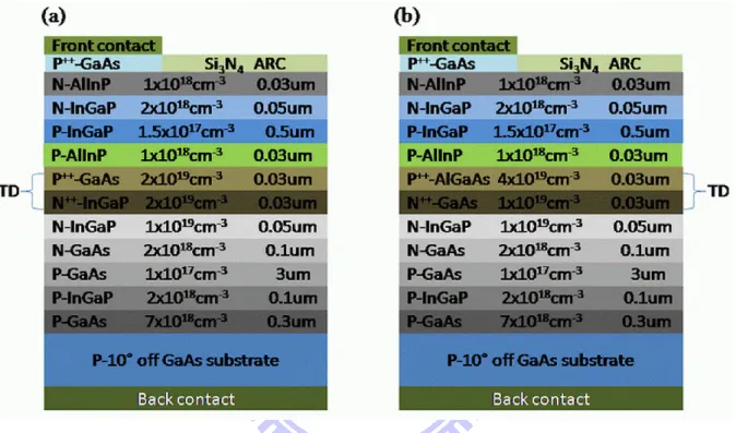
materials: (a) the cell design with P++-GaAs/N++-InGaP, (b) the cell design with
P++-AlGaAs/N++-GaAs ………. 53
Fig. 4-6 The current-voltage (I-V) characteristics of InGaP/GaAs dual-junction solar cells measured at one sun. Sample A: the cell design with a P++-GaAs/N++-InGaP tunnel diode (TD) grown on 10° off misorientation GaAs substrates; sample B: the cell design with a P++-AlGaAs/N++-GaAs TD grown on 10° off misorientation GaAs substrates; sample C: the cell design with a P++-GaAs/N++-InGaP TD grown on 6° off misorientation GaAs substrates ………. 54 Fig. 4-7 External quantum efficiency (EQE) of InGaP/GaAs dual-junction solar cells. Sample
A: the cell design with a P++-GaAs/N++-InGaP tunnel diode (TD) grown on 10° off misorientation GaAs substrates; sample B: the cell design with a
P++-AlGaAs/N++-GaAs TD grown on 10° off misorientation GaAs substrates; sample C: the cell design with a P++-GaAs/N++-InGaP TD grown on 6° off misorientation GaAs substrates ………. 55 Fig. 4-8 The current-voltage (I-V) characteristics of InGaP/GaAs dual-junction solar cells
operated at higher concentration ratios (185×). Sample A: the cell design with a P++-GaAs/N++-InGaP tunnel diode (TD) grown on 10° off misorientation GaAs substrates; sample B: the cell design with a P++-AlGaAs/N++-GaAs TD grown on 10° off misorientation GaAs substrates; sample C: the cell design with a
P++-GaAs/N++-InGaP TD grown on 6° off misorientation GaAs substrates …….… 56 Fig. 5-1 Anti-pahase formation of polar semiconductor materials on non-polar semiconductor
materails ……… 82 Fig. 5-2 Schematic drawings of GaAs crystal structure ………. 82 Fig. 5-3 The two possible sublattice locations of Ga and As atoms in GaAs grown on Ge
epitaxy ………... 83 Fig. 5-4 Sublattice location phase diagram as a fuction of growth temperature and
disorientation angle for GaAs on Ge (100) off towards (111) ……….. 83 Fig. 5-5 2-D and 3-D AFM topographical images of the GaAs epitaxial layers grown on 6°
off-oriented Ge substrate with growth temperature at (a)(b) (b) 650°C and (c)(d) 750°C ……… 84 Fig. 5-6 TEM images of GaAs grown on Ge substrate with different misorientation angles (a)
xi
Fig. 5-7 A model to explain the reversal of the sublattice locations between GaAs grown on (100) Ge off toward (111) substrates with small and larger misoriented angles. (a) Nucleation on Ge substrate with larger misoriented angles: nuclei form only at steps. (b) Overgrowth on such surface results in that the initial nuclei are connected with each other so that single-phase domain of GaAs-A is achieved. (c) Nucleation on Ge substrate with small misoriented angles: nuclei form at steps and on the terraces.(d) Overgrowth on such surface resultsin that the initial nuclei at the steps are
surrounded by theAPDs ……….... 85 Fig. 5-8 Cross-sectional TEM micrographs of two 1μm thick GaAs films grown on Ge. (a)
Film with high APDs densities extending to the surface, grown on an unannealed epitaxial Ge layer. (b) APD-free film grown on an annealed epitaxial Ge layer ….. 85 Fig. 5-9 (a) SA (upper left) and SB (upper right) single atomic-layer steps. On a mixed domain
surface (bottom) both types of single steps are evident. Note the rotation of
dimerization axes and dimer rows on alternating terraces. (b) DA (upper left) and DB
(upper right) double atomic-layer steps. Note that only DB steps are observed
experimentally, DA steps are energetically unfavorable. On the single-domain surface
(below) the dimerization axis and dimer rows are invariant across the DB step …... 86
Fig. 5-10 Diffusion coefficients and solid solubilities of Ga and As in Ge layer …………... 87 Fig. 5-11 SIMS profiles for GaAs/AlAs/Ge samples with AlAs nominal thickness of (a) 0, (b)
10, (c) 20, and (d) 30 nm. The corresponding TEM image for each sample is placed behind the graph to illustrate the position of the layers ……… 88 Fig. 5-12 All parametrs used in the study are shown in the chart, which include growth
temperature, V/III ratio, substrate annealing temperature, substrate annealing time and growth temperature of As prelayer ……….… 89 Fig. 5-13 AFM images (5μm×5μm) of GaAs layer with different V/III ratios grown on a Ge/Si substrate using a graded-temperature As prelayer (a) V/III: 11, (b) V/III: 20, (c) V/III: 30, (d) V/III: 50, (e) V/III: 75, and (f) V/III: 20 and annealed at 650°C …………... 90 Fig. 5-14 Lateral and vertical growth rates as a function of [AsH3] ………... 91
Fig. 5-15 Schematic cross sections of (a) [110] and (b) [-110] steps ……….. 91 Fig. 5-16 TEM cross-sectional micrograph of GaAs/As/Ge/Si heterostructure grown at a
V/III ratio of 20. (a) unannealed Ge/Si substrate and (b) Ge/Si substrate annealed at 650°C ………... 92 Fig. 5-17 SIMS profiles for GaAs epitaxy grown at different V/III ratios on a Ge/Si substrate with a graded-temperature As prelayer (a) V/III: 20, (b) V/III: 20 and annealed at 650°C ………..… 93 Fig. 5-18 HRXRD rocking curves of the GaAs/As/Ge/Si heterostructure grown at a V/III
ratio of 20. (a) unannealed Ge/Si substrate and (b) Ge/Si substrate annealed at 650°C ……….. 94
xii
Fig. 5-19 SIMS profile of carbon for the GaAs/As epitaxy grown on both the unannealed Ge/Si substrate and the Ge/Si substrate annealed at 650°C ……… 94 Fig. 5-20 SIMS profiles for GaAs epitaxy grown at different V/III ratios on a Ge/Si substrate with a graded-temperature As prelayer (a) V/III: 20, (b) V/III: 30, (c) V/III: 50, (d) V/III: 75, (e) V/III: 20 and annealed at 650°C ……… 95
1
Chapter 1
Introduction
1.1 Brief introduction to photovoltaic industry
Solar energy is one of fastest growing industries in the energy field. Some research reports
that total global new PV system installations reached 18.2GWp in 2010. However, the global
PV market including silicon-base, thin film, organic solar cells, declines rapidly in 2011.
Major reductions in subsidy levels are occurring across the major European PV markets in
2011. As European markets account for 80% of global demand, this will have a decisive effect
on supply and demand in the global PV industry. However, the PV markets of China, India,
America, Australia and other countries also have a great deal of growth momentum, which
could even be sufficient to offset the impact of weakening European demand.
Many PV companies, including silicon-base, III-V thin film solar cells et al., are built in
Taiwan in recent years because of good environment and opportunity. In Taiwan the technique
of semiconductor, panel, electronic component industries is very mature and suitable for
developing photovoltaic industry. Now the investments in PV industry in Taiwan main focus
on Si-base solar cells because these type solar cells possess low cost and low threshold on the
field. The conversion efficiency of commercial crystalline Si solar cells is only about 20%.
Furthermore, Si-base solar cells cannot be operated at higher concentrated system. In order to
2
photovoltaic solar cells, CPVSCs) started in 2005. III-V solar cells (CPVSCs) are a “special
innovation” in PV industry, which is operated under high concentrated ratios and is suitable in
arid places or mid-arid places. III-V solar cell efficiency under high concentrated ratios is
60% in theory and 42% in production, considerably two times higher than traditional Si-based
solar cells as shown in Fig.1-1. The basic properties of concentrated III-V multijunction solar
cells will be discussed in next section.
1.2 Concentrated III-V multijunction solar cells and its challenges
Concentrated Photovoltaic technology uses several optical lenses (Fresnel) to focus large
amounts of sunlight onto small photovoltaic surfaces to generate electricity more efficiently
than traditional PV as show in Fig. 1-2. The greater efficiency comes from the photovoltaic
cells used in CPV, which can be III-V multijunction cells instead of the crystalline silicon
cells used in traditional PV systems. Fig.1-3 shows the typical distribution of solar radiation
on the surface of the earth and if one could design the band gap of the III-V solar cells in a
monolithic multijunction form having multiple semiconductor layers with different band gaps,
the majority of the solar spectrum can be captured by the combination of cells.
Gallium arsenide (GaAs) is often used as middle junction in III-V multijunction solar cells
that have nearly optimal band gap of 1.42eV. The conversion efficiency of GaAs single
3
electric structure, as middle cell in III-V multijunction solar cells can absorb majority of
visible light (~750nm) of solar radiation without any heating generation. Additional, the band
gap distribution of GaAs-based materials, such as indium gallium arsenide (InGaAs), can be
adjusted to absorb other solar energies with different wavelength by varying the elemental
composition. Although III-V multijunction solar cells possess highest conversion efficiency
(42%) in the world and can be operated at concentrator system, they are very expensive and
are currently only used in high performance applications such as satellites and power plants
due to their cost.
All CPV systems have an III-V multijunction solar cell device, a concentrator system
including Fresnel lens and active solar tracking. In order to reduce the cost and increase the
competitiveness of CPV, suncycle concentrator system is used instead of regular concentrator
system in recent work [2] as shown in Fig. 1-4. The suncycle concentrator system is a
compact concentrator solar panel which can be installed as a rooftop unit in both commercial
and residential buildings. It uses optical technology for concentrating sunlight on an III-V
solar cell. Optimization algorithms help to track the movements of the sun, making the most
of the available sunlight. On the other hand, the promotion of conversion efficiency of III-V
multijunction solar cells and the reduction of epitaxial cost during III-V material growth are
also an efficient way to decrease overall CPV cost. The detailed description about decreasing
4
References
[1] M.A. Green, K. Emery, Y. Hishikawa, W. Warta, Solar cell efficiency tables (version 31), Prog. Photovolt: Res. Appl. 16, 61–67 (2008).
[2] Sarah Kurtz," Opportunities and Challenges for Development of a Mature Concentrating Photovoltaic Power Industry" CS MANTECH Conference, May 18th-21st, 2009, Tampa, Florida, USA
5
Figure 1-1 Best research solar cell efficiencies reported by NREL
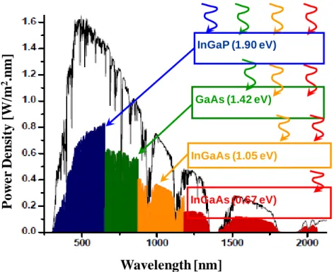
6 GaAs (1.42 eV) InGaAs (1.05 eV) InGaAs (0.67 eV) InGaP (1.90 eV) P ow e r D e n si ty [W/ m 2 .n m] Wavelength [nm]
Figure 1-3 Absorption spectrum of III-V multijunction solar cells with different band gaps
on earth
7
Chapter 2
Development of low-cost high-efficiency III-V solar cells
2.1 Methods for improving efficiency of III-V solar cells
PV energy conversion is the direct production of electrical energy in the form of current
and voltage from electromagnetic (i.e., light) energy. The basic four steps needed for
photovoltaic energy conversion are: (a) a light absorption process which causes a transition in
a material from a ground state to an excited state. (b) the conversion of the excited state into
a free negative-charge and a free positive-charge carrier pair, (c) a discriminating transport
mechanism, which causes the resulting free negative-charge carriers to move in one direction
(to the contact of a cathode) and the resulting free positive-charge carriers to move in another
direction (to the contact of a anode), (d) combining with an arriving positive-charge carrier,
thereby returning the absorber to the ground state. In order to improve the conversion
efficiency of III-V multijunction solar cells, we have to know these basic fundamental and
find out some materials or methods to enhance the solar cell efficiency. Here, some methods
for increasing the conversion efficiency will be generalized and shown in the following.
(A) Antireflection coating (AR coating) or surface texture: a structured surface of III-V
multijunction solar cells enhances the optical path length and reduces the optical reflection
while light inject into solar cell devices.
8
by large currents (Jsc) decrease the conversion efficiency of III-V multijunction solar cells
under high concentration ratios. Rs becomes a dominant factor of cell efficiency with
increasing current. If shunt resistance (Rsh) of III-V solar cells is sufficiently large to be
neglected, the I–V characteristics of the solar cells including series resistance (Rs) are
shown in equation (2.1):
(2.1)
Therefore, the contact resistance has to be reduced sufficiently using optimal N-GaAs
contact material and P-Ge contact material to minimize series resistance losses when III-V
solar cells was operated for concentrator applications.
(C) High Epitaxial quality for III-V solar cell devices: the I-V characteristic of III-V solar
cell devices mainly depends on superior epitaxial quality. For III-V solar cell devices, the
poor quality results in smaller shunt resistance which decreases open-current voltage (Voc).
Besides, structure of III-V multijunction solar cells include back surface field (BSF) layer,
base layer, emitter layer, window layer and tunnel diode (TD) grown between two
subcells. It is more complicated than other devices; therefore, the growth technology is
very important per united component of III-V solar cell devices to further increase
conversion efficiency.
(D) Substrates: The growth of III-V solar cell devices has been restricted to lattice matched,
9
material of choice for commercial III-V solar cell devices because it offers the opportunity
to form a bottom photovoltaic junction as well as being more powerful in production cost
as compared with GaAs substrate, thereby allowing the use of a thinner substrate,
resulting in a lower mass solar cell. Unfortunately, Ge substrate offers no capability to
integrate the finished photovoltaic device into a flexible module and its price still higher
than Si substrate leading to the development limitation of III-V multijunction solar cells.
2.2 Tunnel diode development in III-V multijunction solar cells
Tunnel diode (TD) is one of the important issues affecting III-V multijunction solar cell
performance. The problems of TD growth are related to the demand of obtaining transparent
and uniformly highly doped layer without degradation of surface morphology. The thickness
of the TD has to be about several ten nanometers, while the doping concentration have to be
achieved around 1019-1020 cm-3. The reaching of the high doping level is complicated by the
fact that P-type and N-type dopant (i.e., SiH4, DeTe, TMZn, CBr4…) may require different
growth temperature and growth parameters, making more difficult to obtain abrupt doping
profile. Because of high doping concentration in TD material the interdiffusion from TD to
BSF layer have to be avoided. The double heterostructure (DH) TD was found to be useful for
suppressing unwanted interdiffusion from the tunnel diode [1-3]. On the other hand, the
10
replace other dopants during the TD growth. Once an abrupt doping profile is obtained, the
TD in III-V multijunction solar cells must resist to the thermal load produced by the growth
cycle of the solar cell structure. The detailed description for obtaining high quality TD
without any interdiffusion will be shown in chapter 3 and then InGaP/GaAs dual junction
solar cells with different TD materials will be also discussed in chapter 4.
2.3 Integration of III-V material on Si substrate
Currently, the installation of III-V multijunction solar cells (InGaP/InGaAs/Ge) is limited
by the relatively high cost of III-V solar cells as compared to silicon-based solar cells [4].
Therefore, the integration of the GaAs/Ge heterostructure on Si substrates as an alternative
template for low cost and high conversion efficiency III-V based solar cells has attracted
much attention [5,6]. Si has many advantages as compared to traditional Ge and GaAs
substrates that contain higher thermal conductivity, lower weight, lower cost, and extensive
development to solar cell processes using traditional Silicon-base process technologies. For
terrestrial solar cells, a graded SiGe interlayer as buffer layer is often grown on Si substrate to
relax strains because of larger lattice mismatch (4.2%) between Si and Ge generates many
dislocations in the deposited Ge layer [7]. In this thesis, we have cooperation with Dr.
Yamamoto in Innovations for High Performance Microelectronics (IHP), Germany. Low
11
buffer layer by Yuji Yamamoto et al. using reduced pressure chemical vapor deposition
(RPCVD) [8]. Low TDD of ~7×105cm-2 is achieved for 4.7μm Ge thick layer with a lower
surface roughness (RMS~0.44nm). If III-V multijunction solar cells can be grown on Ge/Si
substrate using GaAs-base buffer layer to replace traditional InGaP/(In)GaAs/Ge solar cells,
the cost of CPVSCs will be further decreased. The detailed description for III-V material
(GaAs) on Ge/Si substrate will be shown in chapter 5.
2.4 Motivation
The development of an advanced technique that can enhance photovoltaic conversion
efficiency while maintaining the lower APD formation and depressed interdiffusion in the
GaAs/Ge system is necessary for the development of low-cost and high-efficiency III-V
12
References
[1] Masafumi Yamaguchi and Antonio Luque, IEEE TRANSACTIONS ON ELECTRON DEVICES 46, 2139 (1999)
[2] Mathieu Baudrit and Carlos Algora, Phys. Status Solidi A 207, 474 (2011)
[3] I. Garcia, I. Rey-Stolle, B. Galiana, and C. Algora, Appl. Phys. Lett. 95, 053509 (2009) [4] Masafumi Yamaguchi, Tatsuya Takamoto and Kenji Araki, Solar Energy Materials & Solar
Cells 90, 3068 (2006)
[5] Carrie L. Andre, John A. Carlin, John J. Boeckl, David M. Wilt, M. A. Smith, A. J. Pitera, M. L. Lee, Eugene A. Fitzgerald, and and Steven A. Ringel, IEEE TRANSACTIONS ON ELECTRON DEVICES, 52, 1055 (2005)
[6] M. R. Lueck, C. L. Andre, A. J. Pitera, M. L. Lee, E. A. Fitzgerald, and S. A. Ringel, IEEE TRANSACTIONS ON ELECTRON DEVICES, 27, 142 (2006)
[7] D. J. Friedman, S. R. Kurtz, and J. F. Geisz, "Analysis of the GaInP/GaAs/1-eV/Ge cell and related structures for terrestrial concentrator applications," in Proc. 29th IEEE Photov. Spec. Conf., 2002, pp. 856-859
[8] Yuji Yamamoto, Peter Zaumseil, Tzanimir Arguirov, Martin Kittler, Bernd Tillack, Solid-state electronics 60, 2 (2011)
13
Chapter 3
Effect of Substrate Misorientation on the Material Properties of GaAs/
Al
0.3Ga
0.7As Tunnel Diodes
3.1 Principles of a tunnel diode
A tunnel diode (TD) forms the electrical connection between two subcells in multijunction
photovoltaic cells where electrons tunnel from occupied energy states on N++ side of the
barrier to unoccupied energy states on the P++ side. The current density of a tunneling diode is
composed of three components as shown in equation (3.1) and the current-voltage (I-V)
characteristics for a tunnel diode is shown in Fig. 3-1.
J= Jtunnel +Jexcess + Jthermal (3.1)
These components are Jtunnel, the band-to-band tunneling current density, Jexcess, the excess
current density, and Jthermal, the minority-carrier diffusion current density or thermal current
density. The forward bias of a tunnel diode is increased from zero, the quantum mechanical
tunneling leads to an increase of current at first. It reached a peak value and then decreases.
Combining the forward diode characteristic with the tunneling curve yields an idealized
characteristic as shown by the solid line in Fig. 3-1.
The band-to-band current component is shown in Eq. (3.2)
(3.2)
14
negative differential resistance region, respectively. The maximum value of tunneling current
occurs at Vpeak = (Vn+Vp)/3. The detailed equation in the term Vpeak has been determined to be
in Eq. (3.3).
(3.3)
where Vn is the amount of degeneracy on the n side, [Vn = (EFn-Ec)/q], where EFn is the
electron quasi-Fermi energy and Ec is the conduction band energy. Vp is the amount of
degeneracy on the P side, [Vp= (Ev- EFp)/q], where EFp is the hole quasi-Fermi energy and Ep
is the valance band energy. kB is Boltzmann’s constant, T is the temperature, q is the charge,
Nd is the donor concentration, Na is the acceptor concentration, Nc is the effective density of
states in the conduction band. Actually, the probability of band-to-band tunneling decreases
with an increase in the forward bias because of the decrease of the field term. Hence the
peak-current point shifts to the left and occurs at a lower voltage.
The second component is excess current shown in the valley region (in Fig. 3-1). There is
a minimum current point in the region where the tunneling characteristic meets the
forward-diode characteristic. In this idealized curve, the current at this minimum point can be
very small. The ratio of peak tunneling current to the valley point can be very high. There is a
certain amount of “excess” current which raises the minimum current to such a value that the
practical peak-current-to valley-current ratio is in the order of 10 to 20. They are not
15
component is:
(3.4)
where Jvalley is the current density and Vvalley is the voltage at the end of the negative
differential resistance region. The excess current component is the most difficult term to
determine theoretically because a high degree of knowledge of the growth conditions and
environment must be known and quantified, so effects, such as from traps and dislocations,
are known prior to device growth. This current joins the exponential excess current and the
direct tunneling current and forms a smooth but higher valley. Brody [1] suggested that the
valley excess current was caused by tunneling between tailing states which have been
separated from the band edge by the heavy doping.
The third component is thermal or minority carrier diffusion current shown in Eq. (3.5)
and Fig. 3-1.
(3.5)
where
(3.6) where ni is the intrinsic carrier concentration, Dn is the electron drift diffusion coefficient, Dp
16
Detailed descriptions of the band diagram and IV characteristics in various states of
operation of a tunnel junction are shown in Fig. 3-2. Figure 3-2(a) shows the reverse-biased
configuration. Electrons can tunnel easily from p-type side to n-type side when tunnel diodes
was operated at larger the reverse-bias. Figure 3-2(b) shows the device in thermal equilibrium.
The Fermi-level is the same for n-type and p-type material and no net current is generated
under this condition. Figure 3-2(c) shows the band-to-band tunneling. As the forward bias is
increased, more occupied states on the electron side coincide with unoccupied states on the
hole side. This occurs up to a maximum tunneling current where EFn − EV = EC − EFn as
shown in Figure 3-2(d). Figure 3-2(e) shows negative differential resistivity (NDR) region
where the overlap of occupied states on the electron side and the unoccupied states on the
hole side decreases to a point where there is no longer any overlap between the two. The
current does not go to zero because the excess current component is non-negligible. Figure
3-2 (f) shows minority-carrier injection current or thermal current as obtained in standard p-n
junction diodes.
For an actual tunnel diode, there is also the substance resistance and the contact resistance
of the loads. These resistances occur in series with the diode and modify the I-V curve by
shifting the high current portion of the characteristic to a higher voltage. This modification is
more noticeable at the peak-current point (Ipeak), where a small increase of voltage can be a
17
the series resistance [2].
3.2 Properties of GaAs/Al0.3Ga0.7As tunnel diode
AlGaAs epitaxy is potentially of great important for many high-speed electronics and
optoelectronic devices [3,4], because the lattice parameter different between GaAs and
AlGaAs is very small, which avoids the generation of undesirable interface states. AlGaAs
epitaxy with excellent minority carrier mirror properties in optoelectronic devices may be also
used for the P-type material due to stronger bonding strength between Alumina (Al) atoms
and carbon (C) atoms, avoiding the high optical absorption of P-type GaAs. Therefore,
GaAs/AlGaAs heterostructure is very suitable as tunnel diode (TD) materials for III-V solar
cell application.
The use of heterojunction TD (GaAs/AlxGa1-xAs) with higher conduction band also
offset[5] provides higher tunneling current (Jtunnel) as compared to the traditional GaAs/GaAs
TD structure. However, AlxGa1-xAs epi-layers are known to be sensitive to oxygen and carbon
impurities, which produces excess current (Jexcess) via energy states inside the band gap. It has
been reported that the reduction of these impurities from an AlGaAs epi-layer can be achieved
using shorter growth interruption [6], liquid metal bubblers [7] and (311) oriented GaAs
substrates [8,9]. But it is difficult to use these methods for commercial applications because of
18
Alternatively, oxygen incorporation in AlGaAs can also be reduced by using a higher
growth temperature (> 750°) and a higher V/III ratio. However, the increase of growth
temperature and V/III ratio will lead to the reduction of carbon doping level during the
GaAs/AlxGa1-xAs TDgrowth [10,11]. Therefore, the development of an advanced technique
which decreases oxygen-incorporation while maintaining high carbon doping in P++-AlGaAs
is necessary for the GaAs/AlxGa1-xAs TD application.
3.3 Growth of GaAs/ Al0.3Ga0.7As heterostructure on misoriented GaAs substrates
Misoriented GaAs substrate is widely used to produce the optimum surface morphologies
for essentially all V/III semiconductors, including GaAs. Furthermore, Kuech and Veuhoff [12]
found that a effect of substrate morientation on carbon incorporation that they contributed to
the increased affinity of CH3 radicals for electron-rich As surface. J. van de van et al. [13] also
reported a significant increase in mobility as well as the net carrier concentration due to a
decrease in the carbon concentration as the misorientation angle was increased form 0° to 4°.
A expected mechanism is related to the reaction velocity of the steps on the surface at which
atoms are incorporated during material growth [13]. For small misorientation, the number of
steps is small, resulting in a large reaction velocity on the surface. The repidly moving steps “trap” carbon before it can interact with atomic H. The trapped “CH3” radical is suggested to
19
atom into the solid. Increasing the misorientation may increase the number of steps on the
surface. This leads to an increased time for interaction of CH3 adsorbed to a Ga at a step with
AsH, producing CH4. Similar behavior is also observed for [110] and [-110] oriented steps, as
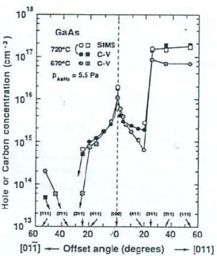
shown in Fig. 3-4. An alternate explanation is related to the rate of production of atomic H on
the surface from the pyrolysis of AsH3 [14]. The presence of surface steps and kinks is
postulated to increase the AsH3 pyrolysis rate and the local production of H and AsH species
on the surface that react with CH3 to produce CH4. This will, of course, reduce the rate of
carbon incorporation into the solid.
An abrupt increase in carbon incorporation is observed for (311)A substrate orientation.
High carbon incorporation for this orientation has also been observed for AlGaAs [14] and
InGaAs [15]. This suggests that (311)A substrate orientation possesses higher step density
which leads to highest AsH3 local pyrolysis rate and a minimal amount of carbon
incorporation. It proves that misorientated substrates have been used to reduce the background
carbon concentration in undoped GaAs epitaxial layers [12,13]. Recently, this concept is also
used in undoped GaAs/Al0.3Ga0.7As quantum well in order to obtain superior surface
morphology and optical properties by using substrates with small misorientation angles, i.e.
from 0~0.6°[16]. Although there have been a number of reports on the impurity-incorporation
in GaAs and AlGaAs [12~14,16], the properties and impurity incorporation mechanism of the
20
3.4 Experiment
In this part, we report on the investigation of the growth of GaAs/Al0.3Ga0.7As TDs on
misorientated substrates for multijunction III-V solar cell applications. The (100) substrates
were cut 0°, 2°. 6°, 10°,15° off toward the [111] direction. The structure used in the study was
N++-GaAs(1~3x1019cm-3, 30~40nm)/P++-Al0.3Ga0.7As(1~5x1019cm-3, 30~40nm) with GaAs as
the buffer layer. Growth is performed with metal organic chemical vapor deposition
(MOCVD, EMCORE D180) system. Trimethylgallium (TMG) and trimethylaluminum
(TMAl) were used as group III source, whereas pure arsine (AsH3) with low H2O content was
used as group V source. The precursors for P-type and N-type dopant were
carbon-tetrabromide (CBr4) and dimethyl-telluride (DMTe), respectively. The growth
temperature was varied from 600℃to 640℃ and was determined by PYRO sensors. The V/III
ratios used were 45 and 12 for the growth of GaAs and Al0.3Ga0.7As, respectively. All films in
this study were grown at low-pressure of 40 torr with hydrogen flow rate of 28000sccm.
Atomic Force Microscopy (AFM) was used to investigate the surface morphology and
roughness of the GaAs/Al0.3Ga0.7As TDs; Secondary Ion Mass Spectrometry (SIMS) was used
to identify the dopant distribution and the relative impurity contents in the GaAs/Al0.3Ga0.7As
TDs. The crystalline quality and carbon-incorporation of the GaAs/Al0.3Ga0.7As TDs were
21
3.5 Results and discussion
3.5.1 Effect of substrate misorientation on the surface morphologies of GaAs/AlGaAs
Tunnel diodes
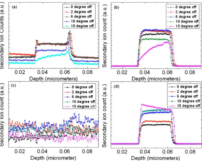
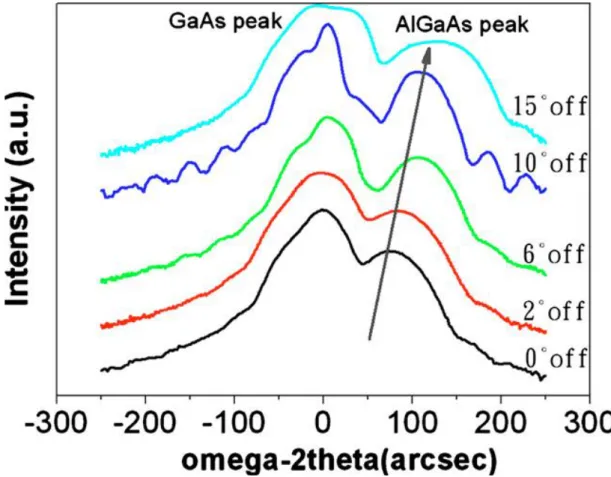
Figure 3-5 illustrates the AFM images of GaAs/Al0.3Ga0.7As TDs grown on GaAs
substrates with different misorientation angles. The root mean square (RMS) roughness of
GaAs/Al0.3Ga0.7As TDs grown on 0°, 2°, 6°, 10°,15° off oriented GaAs substrates were about
1.23 Å , 1.52 Å , 2.03 Å , 1.54 Å , and 2.74Å , respectively. The TD surface morphology is
closely related to the substrate orientation, film thickness, film composition, dopant type, and
doping concentration. The thickness and dopant type were constant for all samples in this
study. According to the AFM results, the GaAs/Al0.3Ga0.7As TDs grown on 0°, 2° and 10° off
GaAs substrates have smoother surface. The rougher surface morphology for GaAs/AlGaAs
TDs grown at other misorientation angles may be caused by the following reasons. First, the
dopant diffusion in heavily doped GaAs/Al0.3Ga0.7As layers may lead to the degradation of the
morphology of the epitaxial layers [17]. Secondly, the surface also becomes rougher with the
increase of Al composition in AlxGa1-xAs layer, especially for x=15~45% [18]. Finally, the
increase of oxygen-incorporation into GaAs layer may also further reduce the surface
smoothness of a GaAs/AlGaAs heterostructure [19]. S. Nayak et al. [19] reported that surface
roughness of GaAs epitaxy decreases with increase of oxygen doping concentration during
22
affected, consisting of 3D clusters, by a bulk oxygen doping concentration of larger than
1019cm-3. There are many factors that can affect the surface morphology of GaAs/AlGaAs TD;
therefore, we will further discuss the relationship between impurity and epitaxial quality for
GaAs/AlGaAs TD grown on misorientated GaAs substrate.
3.5.2 The properties and impurity incorporation mechanism of the GaAs/AlGaAs
tunnel diodes grown on misorientated GaAs substrates
Figure 3-7(a) illustrates the SIMS depth profiles of oxygen in the GaAs/Al0.3Ga0.7As TD
layers grown on GaAs substrates with different misorientations. Oxygen is known as deep
acceptor and non-radiative trap, which decreases the tunneling probability of electrons in
GaAs/Al0.3Ga0.7As TDs. In this study, it is found that oxygen atoms in the heavily doped
GaAs/Al0.3Ga0.7As TDs are mobile enough to segregate at the surface, or be trapped at the
interface [20,21]. The SIMS data also indicates that less oxygen contamination was found in
the P++-AlGaAs layer grown on 10° off GaAs substrates as compared to those grown on other
misorientations. The amount of impurity in AlGaAs depends on Al content [22] and
availability of anisotropic sites [23]. The anisotropic sites possess high affinity for
contaminant incorporation. The variations of Al content in P++-AlGaAs layer are displayed in
Fig. 3-7(b). It indicates a sharp increment in Al content when the GaAs/Al0.3Ga0.7As TDs
23
not follow the initial Al content increment and it suggests that the existence of anisotropic
sites is a more important factor than Al content for oxygen-incorporation in the P++-AlGaAs
layer. The use of 10° off GaAs substrate can practically reduce the anisotropic sites; therefore,
it is a practical technique besides the increase of growth temperature and V/III ratio, to
suppress the oxygen-incorporation in P++-AlGaAs layer of a GaAs/Al0.3Ga0.7As TD.
According to the SIMS and AFM results, the surface morphology of a GaAs/Al0.3Ga0.7As
TD was not affected by the dopant elements because carbon and tellurium as P type and N
type dopant atoms are less mobile during the III-V film growth. The reason for the
degradation of the GaAs/Al0.3Ga0.7As TD surface morphology is mainly due to higher oxygen
content in the N++-GaAs layer [19], as shown in Figure 3-7(a). The substrates with larger
offcut, such as 10°, have more Ga atoms exposed on the surface. They can effectively reduce
the number of As vacancies on the surface and thus reduce the sticking coefficient for oxygen
incorporation [21]. Moreover, smoother surface is also observed for material grown on small
misorientations, such as 0°, which have higher oxygen contamination as compared to 10° off,
due to the Gibbs-Helmholtz surface free energy [24]. The surface free energy increases with
the substrate misorientation angle. Higher misorientation angles imply the existence of a
quasi-liquid layer during material growth, leading to an unstable morphology with a
hill-and-valley structure on the top surface [25]. These results demonstrated in Fig. 3-5 and
24
oxygen-impurity in the N++-GaAs layers but also reduce Gibbs-Helmholtz surface free energy
to produce a smooth surface on the GaAs/Al0.3Ga0.7As TDs.
Figure 3-8 illustrates the HRXRD results of the GaAs/Al0.3Ga0.7As TDs grown on
different misorientation GaAs substrates. The lattice contraction model [26] describes the
relationship of lattice constant variation as a function of carbon-incorporation as shown in
equation (3-7):
△a=NCAs (rc-rAs)(1+ρ) (3-7)
where △a is lattice constant variation; NCAs is the density of carbon atoms on the arsenic sites;
rc and rAs are the covalent radii of carbon (0.774 Å ) and arsenic (1.225Å), respectively; ρ is
the compensation ratio of NCGa/NCAs; NCGa is the density of carbon atoms on Ga sites.
Equation (3-7) shows that the carbon-incorporation may induce the lattice contraction [26,27].
Substitutional carbon atoms in the lattice of the GaAs/AlGaAs heterostructure will reduce the
mean lattice constant of the structure. The observed peak splitting for AlGaAs XRD peaks as
shown in Fig. 3.8 increases with the increasing misorientation angle, meaning that these
spectra are carbon-incorporation related [27]. It demonstrates that carbon doping efficiency,
not the background carbon doping, increases with the increase of the misorientation angle
during the GaAs/Al0.3Ga0.7As TDs growth. The same trend can be observed for the carbon
concentration in the AlGaAs layers grown with different misorientation angles, as shown in
25
occupy the Ga sites rather than Al sites due to the stronger Al-C bond (66Kcal/mole) as
compared to the Ga-C bond (59Kcal/mole) [18,28]. However, the Al content in the 15° off
GaAs substrate decreases rapidly, but the Ga content does not have apparent change during
the P++-Al0.3Ga0.7As growth, as can be observed in Fig. 3-7(b) and (c). It is believed from
these data that the bonding strength between Al-C and Ga-C could be changed [29] and
substitutional carbon would be incorporated in the Al sites resulting in the reduction of Al
composition of a GaAs/Al0.3Ga0.7As TD when the 15° off substrates were used.
3.6 Summary
It has been demonstrated that the misorientation of GaAs substrates has a direct effect on
the material properties of the N++-GaAs/P++-AlGaAs TDs for multijunction III-V solar cell
application. The best surface morphology and interface sharpness for the TDs were obtained
on the (100) tilted 10° off toward [111] GaAs substrate. Results show that the TD materials
grown on this misoriented substrate can overcome the limitation of high surface free energy
and with reduced sticking coefficient for oxygen-incorporation in the N++-GaAs layers.
Besides, this substrate has also reduced the anisotropic sites for oxygen-incorporation in the
P++-AlGaAs layers. These results can be used for the growth of inverted metamorphic
multijunction solar cell structures, which is built on GaAs based substrates and inverted onto
26
References
[1] Brody, T. P., J. appl. Phys. 32, 746 (1961)
[2] Wolfgang Guter and Andreas W. Bett, IEEE TRANSACTIONS ON ELECTRON DEVICES 53, 2216 (2006)
[3] Lassana Ouattara, Anders Mikkelsen, Niklas Skold, Jessica Eriksson, Thijs Knaapen, Elizabeta CÄ avar, Werner Seifert, Lars Samuelson, and Edvin Lundgren, Nano letters 7, 2859 (2007)
[4] Ken Takahashi, Shigeki Yamada, Yasushi Minagawa, and Tsunehiro Unno, Solar Energy Materials & Solar Cells 66, 517 (2001)
[5] John R. Hauser, Zach Carlin, and S. M. Bedair, Appl. Phys. Lett. 97, 042111 (2010) [6] Y. Kadoya, H. Noge, T. Someya, and H. Sakaki, Appl. Phys. Lett. 70, 595 (1997) [7] J. R. shealey and J. M. Woodall, Appl. Phys. Lett. 41, 88 (1982)
[8] K. Tamamura, J. Ogawa, K. Akimoto, Y. Mori, and C. Kojima, Appl. Phys. Lett. 50, 1149 (1987)
[9] T. E. Lamas, A. A. Ouivy, C. S. Sergio, G. M. Gusev, and J. C. Portal, J. Appl. Phys. 97, 076107 (2005)
[10] T. F. Kuech, M. A. Tischler, P. J. Wang, G. Scilla, R. Potemski, and F. Cardone, Appl. Phys. Lett. 53, 1317 (1988)
[11] T. F. Kuech, R. Potemski, F. Cardone, and G. Scilla, J. Electron. Mater. 21, 341 (1992) [12] T. F. kuech and E. Veuhoff, J. Crys. Growth 68, 148 (1984)
[13] J. van de Ven, H. G. Schoot, and L. J. Giling, J. Appl. Phys. 60, 1648 (1986) [14] M. Kondo and T. Tanahashi, J. Crys. Growth 145, 390 (1994)
[15] H. Ito, K. Kurishima, and N. Watanabe, J. Crys. Growth 158, 430 (1996)
[16] N. Moret,a_ D. Y. Oberli, E. Pelucchi, N. Gogneau, A. Rudra, and E. Kapon, Appl. Phys. Lett. 88, 141917 (2006)
27
[18] B. Kim, M. Yoon, J. Son, B. Kim, J. Jhin, and D. Byum, Phys. Stat. sol. (b) 241, 2726 (2004)
[19] S. Nayak, J. W. Huang, J. M. Redwing, D. E. Savage, M. G. Lagally, and T. F. Kuech, Appl. Phys. Lett. 68, 1270 (1996)
[20] M. T. Asom, S. N. G. Chu, M. Geva, and R. E. Leibenguth, Appl. Phys. Lett. 59, 976 (1991)
[21] N. Chand, A. S. Jordan, and S. N. G. Chu, Appl. Phys. Lett. 59, 3270 (1991)
[22] K. S. Zhuravlev, A. I. Toropov, T. S. Shamirzaev, and A. K. Bakarov, Appl. Phys. Lett. 76, 1131 (2000)
[23] D. C. Radulescu, G. W. Wicks, W. J. Schaff, A. R. Calawa, and L. F. Eastman, J. Appl. Phys. 63, 5115 (1988)
[24] C. Herring, Phys. Rev. 82, 87 (1951)
[25] J. Q. Broughton and G. H. Gilmer, J. Phys. Chem. 91, 6347 (1987)
[26] W. E. Hoke, P. J. Lemonias, D. G. Weir, H. T. Hendriks, and G. S. Jackson, J. Appl. Phys. 69, 511 (1991)
[27] Y. Mols, M. R. Leys, E. Simons, J. Poortmans, and G. Borghs, J. Crys. Growth 298, 758 (2007)
[28] T. F. Kuech and J. M. Redwing, J. Crys. Growth 145, 382 (1994)
[29] Chang-Sik Son, Seong-Il Kim, Yong Kim, Young K. Park, Eun Kyu Kim, and Suk-Ki
Min, J. Appl. Phys. 82, 1205 (1997)
[30] J. F. Geisz, Sarah Kurtz, M.W. Wanlass, J. S. Ward, A. Duda, D. J. Friedman, J. M. Olson,
28
Table 3-1 Surface rms roughness (ρ in nm) and wavelength of periodic (λ in nm) surface
structure in 1μm thick GaAs (001) with several concentrations of O are shown. The λ and amplitude (A in nm) are shown up to 1018 cm-3 [O] in GaAs. The breakdown of periodic
29
Figure 3-1 Diagram of I-V characteristics of a tunnel diode including three components [1]
Figure 3-2 Diagram of a tunnel diode (a) reverse-biased tunneling, (b) thermal equilibrium, (c)
forward-biased tunneling, (d) maximum forward-biased tunneling current, (e) negative differential resistance, (f) minority-carrier injection current.
30
Figure 3-3 Equivalent circuit diagram of a test structure with isolated tunnel diode. An
additional resistor RS was used to simulate high internal serial resistances. Right: Influence of
internal serial resistance on the I–V characteristic of a GaAs tunnel diode. The graph with RS
= 0 Ω shows the I–V characteristic of the tunnel diode used. Increasing RS (1 Ω) leads to a
sheared I–V curve and then results in a discontinuity (10 Ω). Very high RS (13 Ω) finally
31
Figure 3-4 Dependence of hole or carbon concentration on orientation for GaAs. Square
32
Figure 3-5 The AFM images (5μm×5μm) of GaAs/Al0.3Ga0.7As TDgrown on GaAs substrates
33
Figure 3-6 AFM images of oxygen doped GaAs; (a) nominally undoped, (b) 1016, (c) 1018, and (d) 1020 cm-3. A periodic ripple structure in the miscut direction is established through step bunching for all but the highest doping levels. The ripple wavelength decreases as [O]
34
Figure 3-7 Depth profiles of (a) oxygen impurity, (b) aluminum and (c) gallium (d) carbon
35
Figure 3-8 HRXRD rocking curves of GaAs/Al0.3Ga0.7As TDs grown on misoriented GaAs
36
Chapter 4
An In
0.5Ga
0.5P/GaAs Dual-junction Solar Cell with GaAs/AlGaAs Tunnel
Diodes Grown on 10° off Misorientation GaAs Substrates
4.1 Introduction
The InGaP/GaAs lattice-matched system has gained significant attention in recent years
for high-efficiency solar cells in both space and terrestrial applications [1,2]. The tandem
combination of an optically thin InGaP top cell and a GaAs bottom cell has a theoretical
efficiency of 34%. The real conversion efficiency of InGaP/GaAs dual-junction solar cells has
been improved to close to 30% in the last decade [3,4]. J. W. Leem et al. [5] reported that the
short-circuit current density (Jsc) of InGaP/GaAs dual-junction solar cells is strongly
dependent on the top and bottom cell thicknesses. As the base thickness of the top InGaP cell
in an InGaP/GaAs dual-junction solar cell with GaAs/GaAs tunnel diode (TD) becomes
thicker, the Jsc is increased for the top cell, whereas the Jsc in the bottom cell is decreased, as
shown in Fig.4-1.This implies that thicker base thickness for InGaP top cell can enhance light
absorption, and thus increase Jsc for a InGaP/GaAs dual-junction solar cell. The base thickness
of GaAs (bottom) cell is optimized at 2~3μm, allowing the maximized current matching
values for both AM1.5G and AM0 illuminations.
Besides, for InGaP/GaAs dual-junction solar cells, the fabrication of effective and stable
37
of the TD structure and the current matching between InGaP top cell and GaAs bottom cell
should be optimized through numerical modeling including TD to achieve high conversion
efficiency [7]. The conversion efficiency of InGaP/GaAs dual-junction solar cells with
different TD structure was also simulated for by J. W. Leem et al. [5]. Figure 4-2 shows the
short-circuit current density (Jsc) as a function of the base thickness of top InGaP cell in a
InGaP/GaAs dual-junction solar cell with InGaP/InGaP TD for the AM1.5G and AM0 solar
spectra. With InGaP/InGaP TD, the Jsc is increased to 10.7mA/cm2 for AM1.5G
(13.69mA/cm2 for AM0) as compared with Fig. 4-1. The wideband gap TD, such as
InGaP/InGaP homostructure, does not absorb incident light in the long wavelength region
compared to GaAs/GaAs TD. Therefore, higher Jsc can be achieved in an InGaP/GaAs
dual-junction solar cell with higher band-gap TD. This concept is matched with Takamoto et
al. [8], they reported that thin and wide band gap TD is necessary for III-V multijunction solar
cell to minimize optical absorption and increase tunnel peak current density (Jtunnel), as shown
in Fig. 4-3.
However, homostructure TD, such as GaAs/GaAs or InGaP/InGaP, is not suitable for
III-V multijunction solar cell due to smaller conduction band offset. The detailed reason will
be discussed in the following. The basic theory of pn junction tunneling was developed by
Keldysh and Kane [9,10] and the tunneling current density can be expressed as follows:
38
where
In these equations, m* is the tunneling effective mass, W is the tunneling barrier width, EF is
the electric field in the tunneling region, Eb is the tunneling barrier height (equals Eg for
simple case), FC( )and FV( ) are Fermi–Dirac functions for the conduction and valence bands
and ES=min(E1 ,E2) with E1 and E2 the energies measured from the band edges. This equation
(4.1) implies that tunneling current density can be increased with decrease of electron
effective mass, tunneling barrier width and band gap.
Figure 4-4 shows the semiconductor band edges around the junction resulting from such a
numerical calculation for a model tunneling junction with a band gap of 1.9 eV both with and
without a conduction band edge difference [11]. The tunneling width is about 42% of the
classically calculated depletion layer width, as shown in Fig. 4-4. Also it is seen that the
tunneling width is reduced when a conduction band offset exists. The AlGaAs/GaAs
heterostructure itself possesses larger energy-band difference in the conduction band than the
39
tunneling current. This implies that heterostructure TD, such as AlGaAs/GaAs, with higher
conduction band offset is necessary for development of high-efficiency III-V multijunction
solar cells.
As III-V solar cell devices have to be operated at higher concentration ratios, TD is also a
very important component. If, at higher concentrations, the peak current density (Jpeak) in the
TD is lower than the short-circuit current density (Jsc), the overall performance of the III-V
solar cell is dramatically affected. Currently, for III-V multijunction solar cells, wide
band-gap materials with a low electrical resistivity, such as AlGaAs and InGaP, are adopted as
TD materials because of lower optical absorption. In fact, the increase in the band gap of TD
materials made from III-V semiconductors results in a decrease in the tunneling current
density, as shown in Fig. 4-3. This implies that the reduction of impurities in TDs, such as
oxygen atoms that act as a nonradiative trap, plays the dominant role when higher band gap
materials are used.
AlGaAs epitaxy is also potentially of great importance for many high-speed electronic and
optoelectronic devices [13,14], because the difference in the lattice parameter between GaAs
and AlGaAs is very small, and this avoids the generation of undesirable interface states.
However, AlGaAs epitaxy as a TD material is known that to have serious oxygen problem as
compared with InGaP epitaxy for III-V multijunction solar cells. The InGaP TDs show a
40
TDs interface. In chapter 3, we proved that the 10° off misorientation GaAs substrates not
only reduce the oxygen-impurity content in N++-GaAs/P++-AlGaAs TD, but also produce high
quality TD with smooth surface and sharp interface[15]. Although the 10° off misorientation
GaAs substrate has been found efficiently reduce nonradiative traps in N++-GaAs/P++-AlGaAs
TD, a dual-junction solar cell grown on 10° off misorientation GaAs substrates using a
N++-GaAs/P++-AlGaAs TD has not yet been reported.
4.2 Experiment
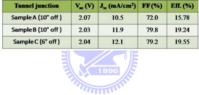
In this part, we report the comparative results of InGaP/GaAs dual-junction solar cells
with a N++-InGaP/P++-GaAs TD (sample A) and with a N++-GaAs/P++-AlGaAs TD (sample B),
both grown on 10° off misorientation GaAs substrates, and also of a N++-InGaP/P++-GaAs TD
grown on 6° off misorientation GaAs substrates (sample C), which have been grown using a
metal organic chemical vapor deposition (MOCVD, EMCORE D180) system.
Trimethylgallium (TMG), trimethylaluminum (TMAl) and trimethylindium (TMIn) were used
as group III sources, whereas arsine (AsH3) and phosphine (PH3) were used as group V
sources. The precursors for p-type and n-type dopants were carbon-tetrabromide (CBr4) and
dimethyl-telluride (DMTe), respectively. For GaAs/AlGaAs TDs, AlGaAs epi-layers may be
easily accomplished higher doping levels with carbon doping compared to GaAs. The GaAs
![Figure 3-1 Diagram of I-V characteristics of a tunnel diode including three components [1]](https://thumb-ap.123doks.com/thumbv2/9libinfo/8205195.169702/43.892.173.768.112.1067/figure-diagram-i-characteristics-tunnel-diode-including-components.webp)

![Figure 4-4 shows the semiconductor band edges around the junction resulting from such a numerical calculation for a model tunneling junction with a band gap of 1.9 eV both with and without a conduction band edge difference [11]](https://thumb-ap.123doks.com/thumbv2/9libinfo/8205195.169702/52.892.284.647.175.449/semiconductor-resulting-numerical-calculation-tunneling-junction-conduction-difference.webp)
![Figure 4-4 Example of junction tunneling width and depletion layer width [11]](https://thumb-ap.123doks.com/thumbv2/9libinfo/8205195.169702/66.892.131.817.223.1031/figure-example-junction-tunneling-width-depletion-layer-width.webp)