國 立 交 通 大 學
電信工程研究所
博 士 論 文
應用於解決
CMOS 閃爍雜訊之低中頻接收
機架構和深
N 型井雙極性接面電晶體直接
降頻接收機
CMOS Flicker Noise Solutions by Low-IF
Receiver Architecture and Deep-N-Well BJT
Direct-Conversion Receiver
研 究 生:徐金詳
指導教授:孟慶宗
型井雙極性接面電晶體直接降頻接收機
CMOS Flicker Noise Solutions by Low-IF Receiver
Architecture and Deep-N-Well BJT Direct-Conversion
Receiver
研究生:徐金詳
Student:
Jin-Siang
Syu
指導教授:孟慶宗 博士 Advisor:
Dr.
Chinchun
Meng
國立交通大學
電信工程研究所
博士論文
A Dissertation
Submitted to Institute of Communication Engineering
College of Electrical and Computer Engineering
National Chiao Tung University
in Partial Fulfillment of the Requirements
for the Degree of Doctor of Philosophy
in
Communication Engineering
Hsinchu, Taiwan
應用於解決
CMOS 閃爍雜訊之低中頻接收機架
構和深
N 型井雙極性接面電晶體直接降頻接收
機
學生:徐金詳 指導教授:孟慶宗博士
Abstract (Chinese)國立交通大學
電信工程研究所博士班
摘
要
本論文中分作五個章節,包含了各式混頻器和接收機之效能改善。在第二章 中提出單頻帶和雙頻帶之高線性度吉伯特升頻器。利用輸入端之偏壓偏移交錯耦 合對與輸出端之並聯回授緩衝放大器,使升頻器之輸出端三階交調截點與輸出端 1-dB 壓縮點差距高達 22 dB。 第三章利用相量表示方式完整地分析和比較各式被動正交信號產生器,包含 了振幅和相位與頻寬的關聯。此外,雙極性接面電晶體之主動混頻器比互補式金 氧半導體之主動或被動混頻器擁有更寬的轉換增益平坦區,因此有著更佳的正交 本地振幅不平衡之容忍度。應用於吉伯特混頻器本地振盪源埠之正交耦合器若直 接在高損耗矽基板上製作,可縮小面積但會有輸出振幅不相等的特性,正好可以 利用選取適當之本地振幅而改善。另一方面,利用 LR-CR 正交相位產生器並配 合雙極性接面電晶體主動混頻器成功地實現一接收機,並且在超寬頻應用頻帶中 輸出端之信號振幅與相位誤差分別低於±1dB 和±2°。 在第四章中,於 0.35 毫米矽鍺異質接面電晶體製程中利用補償相位延遲技 術實作一個高隔離度之次諧波降頻器。在相同偏壓條件、電晶體大小和操作頻率下,使用補償相位延遲技術與傳統無使用此技術之電路可得到相似之轉換增益、 雜訊指數和線性度,卻額外改善了34/35 dB 的 2LO 至 RF/IF 埠隔離度,8/9 dB 的LO 至 RF/IF 埠隔離度和 22 dB 的 RF 至 IF 埠隔離度。 第五章則利用了相量分析方式來討論在雙降頻低中頻接收機中鏡像抑制效 能衰減之原因。因此,分別在射頻輸入端或兩級混頻器中間適當地擺放額外的多 相位濾波器均可以大大地改善鏡像抑制效能,使得在本地振盪源之正交信號誤差 和元件不匹配仍然存在的情況下,達到接近中頻多相位濾波器之鏡像抑制比的理 論極值。 第六章則介紹了在低成本 0.18 毫米互補式金氧半導體製程下應用於低功率 低雜訊直接降頻接收機。在標準互補式金氧半導體製程中,深 N 型井雙極性接 面電晶體因為其超低之閃爍雜訊和較佳之轉導而被有效地應用於混頻器和基頻 放大器中,然而其相對低的截止頻率在混頻器的應用上也造成了額外的挑戰。因 此,透過詳盡地分析操作在低截止頻率之吉伯特混頻器,電感式突起技術被用以 降低本地振盪輸出之損耗和增加混頻器之轉換增益。另一方面,次諧波混頻機制 為另一解決低截止頻率之方式並搭配低損耗的八相位多相位濾波器實作一低功 率低雜訊次諧波直接降頻接收機。最後,利用可調頻式雙級低雜訊放大器和寬頻 之八相位本地振盪產生器,實作了一涵蓋完整 U-NII 頻段之低功率低雜訊接收 機,其中同時利用電感式突起和次諧波混頻機制成功讓接收機之射頻頻率可以為 深N 型井雙極性接面電晶體之三倍截止頻率。 關鍵字:互補式金氧半導體、矽鍺異質接面電晶體、吉伯特混頻器、雙頻帶、次 諧波混頻器、隔離度、低中頻接收機、鏡像抑制、直接降頻接收機、深 N 型井 雙極性電晶體、閃爍雜訊。
CMOS Flicker Noise Solutions by Low-IF
Receiver Architecture and Deep-N-Well BJT
Direct-Conversion Receiver
Student: Jin-Siang Syu Advisor: Chinchun Meng
Abstract (English)
Institute of Communication Engineering
National Chiao Tung University
Abstract
This dissertation consists of five chapters, including performance improvements of various mixer topologies and receivers. Chapter 2 introduces single-/dual-band highly linear Gilbert upconverters. The difference of OIP3 and OP1dB, widely used as a
criterion for mixer linearity, is over 22 dB by using an input bias-offset cross-coupled pair and output shunt-shunt feedback buffer amplifier.
In Chapter 3, passive quadrature signal generators are deeply discussed, including amplitude/phase relations by using phasor analyses. Further, a bipolar-juncion- transistor (BJT)-based Gilbert mixer inherently has a wider flat-gain region and more toleration of LO amplitude imbalance than MOS active/passive mixers. Thus, the loss imbalance of the LO quadrature coupled-line coupler directly implemented on a lossy silicon substrate can be simply solved by choosing proper LO power in the common flat-gain region. On the other hand, an ultra-wideband (UWB) Gilbert downconverter using an LR-CR quadrature generator, which has always perfect quadrature phase but balanced amplitudes only at the center frequency. However, the BJT mixer successfully compensates this drawback and achieves amplitude/phase imbalance
below ±1dB/±2° covering whole UWB bands, respectively.
In Chapter 4, a 0.35-μm SiGe heterojunction bipolar transistor (HBT) high- isolation sub-harmonic mixer is proposed using a delay compensation technique. The sub-harmonic mixers with and without delay compensation are demonstrated at the same bias condition, device sizes and operating frequency. As a result, similar conversion gain, noise figure and linearity are achieved. However, the 2LO-to-RF/IF isolation is improved by 34/35 dB, the LO-to-RF/IF isolation by 8/9 dB and the RF-to-IF isolation by 22 dB.
Chapter 5 fully discusses the reasons for the degradation of the image rejection performance in a dual-conversion low-IF receiver by using phasor analyses. By inserting the poly-phase filters (PPFs) at proper positions (RF stage or inter-stage between two downconversions), the image-rejection ratio (IRR) can nearly reach the theoretical limit of the IF PPF even if the LO quadrature imbalance and device mismatches still exist.
Finally, Chapter 6 introduces various techniques in designing a low-power low-noise direct-conversion receiver (DCR) in a low-cost 0.18-μm CMOS technology. Deep-n-well (DNW) BJTs in standard 0.18-μm CMOS process are used for lower flicker noise and higher transconductance than standard NMOS devices. But the relatively low cut-off frequency (fT) becomes a big challenge for the mixer application.
Thus, the current switching operation of the BJT switching function operating near or even higher than the device fT is fully analyzed. An inductive peaking technique is
then used to compensate the loss of the LO generator and the mixer conversion loss. On the other hand, a sub-harmonic mixing is another straightforward solution for the low-fT operation, but a low-loss octet-phase PPF is analyzed and employed to generate
covering whole U-NII bands is also demonstrated in this chapter by using a two-stage tunable-band RF low-noise amplifier (LNA) and a wideband octet-phase generator.
Keywords: CMOS, SiGe heterojunction bipolar transistor (HBT), Gilbert mixer, dual-band, sub-harmonic mixer, isolation, low-IF receiver, image rejection, direct-conversion receiver (DCR), deep n-well (DNW), bipolar junction transistor (BJT), flicker noise.
Acknowledgements
我與交通大學淵源極深,走過電信工程學系大學四年,而後直升電信研究所 又歷經碩博五年的光陰,隨著這本博士論文的完成,也意味著一段旅程的終點並 即將展開新的旅程。首先要感謝孟慶宗教授的指導,當年學生因電子學課程認識 孟老師,進而有幸成為老師的專題生乃至碩博士研究生。多年來十分感謝老師的 提攜照顧,讓我具備了專業知識以及獨立研究與解決問題的精神。 其次要感謝各位口試委員的指導,讓學生的論文更加充實完備。感謝呂學士 教授、劉深淵教授、李致毅教授、徐碩鴻教授、張盛富教授、張志揚教授、鍾世 忠教授與郭建男教授,遠道而來參與學生的博士論文口試,提供指導與建議;還 要感謝國家晶片系統設計中心提供晶片實作機會,國家奈米元件實驗室高頻技術 中心黃國威博士及其團隊提供量測協助;感謝當年電信系系主任陳伯寧教授,在 學生求學之路遇上瓶頸時,給予溫暖的關心和寶貴的建議,至今學生仍銘記在 心。此外,更特別感謝聯發科技基金會的賞識,提供學生優渥的獎學金,讓學生 能夠專心研究,不因現實生活煩惱。 當初從大學三年級開始參與專題實作,感謝吳智凱、張宇文、吳澤宏、廖樺 輿、顏英杰、張家宏學長在我還懵懂無知時給予我實作上最實質的幫助。正式進 入研究所生活之後,吳宗翰、曾聖哲、魏宏儒學長和蘇珍儀學姐在研究上給予寶 貴的意見以及量測上的經驗,並且與李約廷、欉冠璋、游勝文、吳柏誼學長以及 同學林宜蓁、鄧雅惠、陳揚鮮、李宜珊和陳威宇透過不斷切磋討論一同精進。之 後陸續帶了三屆的學弟妹們進行研究或計畫,其中特別感謝陸熙良、張智凱、林 忠佑、楊雋、吳彥鋒學弟和王嘉苓學妹,在參與公司合作計畫時,除忍受我的急 性子,也盡全力完成各年度的計畫。此外,蕭語鋕、張簡協修、廖偉程、彭國維、 莊格瑋、陳韋學學弟們,雖然沒有太多的機會在研究上互相交流,但由於你們, 讓實驗室生活不會苦悶。感激之情非三言兩語可道盡,相信這段時光將成為我人 生中最深刻的回憶。感謝爸爸、媽媽與哥哥的支持,讓我在求學的路途平順;也要感謝室友及眾 多校內外的朋友們,在我遇到瓶頸或逆境時,可以適時給予我勇氣,並提供抒發 宣洩的管道。要感謝的人太多了,因為有了大家,才能完成求學生涯的研究工作, 願此成果與大家共享。
Jin-Siang Syu
NCTU, June 2011Table of Contents
Abstract (Chinese) ... i
Abstract (English) ... iii
Acknowledgements ... vii
Table of Contents ... ix
List of Figures ... xiii
List of Tables ... xxi
List of Abbreviations ... xxiii
Chapter 1 Introduction ... 1
1.1 Commercial Frequency Bands and Applications ... 1
1.2 Process Chosen ... 3
1.2.1 Cost vs. Performance ... 3
1.2.2 Flicker Noise ... 5
Chapter 2 High Linearity Gilbert Upconversion Mixer ... 7
2.1 High-Linearity Bias-Offset TCA ... 7
2.1.1 Introduction ... 7
2.1.2 Gilbert Upconversion Mixers With NMOS/PMOS Bias-Offset TCA ... 10
2.2 Dual-Band High-Linearity Gilbert Upconversion Mixer ... 17
2.2.1 Dual-Band LC Current Combiner ... 17
2.2.2 Dual-Band Upconversion Mixer With a Dual-Band LC Current Combiner .. 20
2.2.3 2.4/5.7 GHz High-Linearity Gilbert Upconversion Mixer ... 22
Chapter 3 Passive Quadrature Signal Generations and Their Applications on BJT- based Gilbert Mixers ... 27
3.1 Passive Quadrature Signal Generation ... 27
3.1.1 Phasor and Complex Representations for Real Signals ... 28
3.1.2 Distributed Quadrature Signal Generation Method(Quadrature Coupler) 31 3.1.3 Lumped Quadrature Signal Generation Methods ... 33
3.2 Applications on BJT Gilbert Mixers... 40
3.2.1 5.7-GHz I/Q Downconversion Mixers With an LO Quadrature Coupler ... 42 3.2.2 UWB I/Q Downconversion Mixers With an LR-CR Quadrature Generator . 48
Chapter 4 High-Isolation Compensated Sub-Harmonic Mixer ... 57
4.1 Introduction ... 57
4.2 Compensated Stacked-LO Sub-Harmonic Mixer ... 66
4.3 15-GHz SiGe HBT Sub-Harmonic Mixer With Delay Compensation ... 70
Chapter 5 Dual-Conversion Low-IF Receiver With Large Image Rejection ... 77
5.1 Introduction ... 77
5.2 Large Improvement in Image Rejection in Weaver-Hartley Receivers ... 83
5.2.1 Introduction ... 83
5.2.2 Single-Quadrature-Double-Quadrature Architecture With an Inter-Stage Poly-Phase Filter ... 87
5.2.3 Double-Quadrature-Double-Quadrature Architecture With an RF Poly-Phase Filter ... 92
5.2.4 Comparisons and Conclusions ... 97
Chapter 6 Low-Power Low-Noise Direct-Conversion Receiver ... 99
6.1 Introduction ... 99
6.2 Low-Power Design Optimization ... 101
6.2.1 Low-Noise Amplifier Design Optimization With On-Chip Inductors at a Fixed Power Consumption ... 102
6.2.2 Inter-Stage Transformer Design Optimization ... 112
6.2.3 Device Characteristics of Vertical-NPN BJTs ... 115
6.2.4 Variable-Gain Amplifier With Linear-in-dB Tuning Scheme ... 119
6.3 2.4 GHz Receiver With Passive Mixer Realization ... 121
6.4 2.4 GHz Low-Noise Receiver With Vertical-NPN BJT ... 128
6.4.1 2.4 GHz Receiver With Vertical-NPN BJT Operating at Near Cut-Off Frequency ... 128
6.4.2 2.4 GHz Sub-Harmonic Receiver With Multi-Stage Octet-Phase Poly-Phase Filter ... 144
6.4.3 Comparison of the Demonstrated 2.4-GHz Direct-Conversion Receivers 157 6.5 Sub-Harmonic Receiver With Tunable-Band RF LNA and Wideband LO Generator at U-NII Bands... 159
Chapter 7 Conclusion and Future Work ... 179
Appendix A Derivation of the Transimpedance Gain of a Transformer ... 183 Appendix B Derivation of Conversion Gain with Finite Cut-Off Frequency and Gain
Appendix C Derivation of Optimal Inductance for an Inductive Peaking Between LO
Poly-Phase Filter and Mixer Core ... 191
Appendix D Derivation of Amplitude/Phase Relations of a Multi-Stage Octet-Phase Poly-Phase Filter ... 193
Appendix E Derivation of the Peak Gain and the Corresponding Criterion of the LC Tank with Lossy Inductor ... 195
Appendix F Derivation of the Tuning Capability of A Transformer With Only One Varactor in Either Side ... 197
References ... 199
Curriculum Vitae ... 209
List of Figures
Chapter 1
Fig. 1-1 Comparisons for WPAN and WLAN by data rate and distance. ... 2
Fig. 1-2 TSMC Technology Development ... 4
Fig. 1-3 R&D and production cost of CMOS technology for (a)digital IC(b)RFIC. ... 4
Chapter 2 Fig. 2-1 (a) BJT differential amplifier (b) MOS differential amplifier (c) MOS pseudo-differential pair. ... 7
Fig. 2-2 Block diagram of the single-/dual-band Gilbert upconverter. ... 8
Fig. 2-3 Bias-offset transconductance amplifier. ... 9
Fig. 2-4 Schematic of the Gilbert upconverters with NMOS/PMOS-type bias-offset TCAs and a single-band LC current combiner. ... 10
Fig. 2-5 (a)NMOS (b) PMOS I-V characteristics with different gate lengths. ... 11
Fig. 2-6 Block diagram of the LC current combiner and its equivalent circuit at the resonant frequency. ... 13
Fig. 2-7 Die photo of the Gilbert upconverter (a) using an NMOS TCA (b) using a PMOS TCA. ... 14
Fig. 2-8 Conversion gain with respect to RF frequency. ... 14
Fig. 2-9 Power performance. ... 15
Fig. 2-10 IF bandwidth. ... 15
Fig. 2-11 LO-to-RF isolation. ... 15
Fig. 2-12 Operational principle of the dual-band LC current combiner. ... 17
Fig. 2-13 Frequency response of a dual-band LC current combiner. ... 17
Fig. 2-14 Schematic of the 2.4/5.7 GHz Gilbert upconverter with a dual-band LC current combiner. ... 20
Fig. 2-15 Die photo. ... 21
Fig. 2-16 Conversion gain with respect to RF frequency. ... 21
Fig. 2-17 Power performance. ... 21
Fig. 2-18 Schematic of the SiGe BiCMOS dual-band Gilbert upconverter with the bias-offset TCA and dual-band LC current combiner. ... 22
Fig. 2-19 Die photo. ... 23
Fig. 2-20 Conversion gain as a function of RF frequency. ... 24
Fig. 2-21 Conversion gain with respect to LO power at RF=2.4 and 5.7 GHz. ... 24
Chapter 3
Fig. 3-1 (a)Balanced phasor setsR L D , , andI (b) phasor set with amplitude imbalance (ΔA) (c) phasor set with quadrature phase error () (d)
phasor set with both phase and amplitude imbalance. ... 29
Fig. 3-2 Description of the S parameters for a 3-dB quadrature coupler and a high-coupling quadrature coupler. ... 32
Fig. 3-3 (a) RC-CR phase shifter (b) LR-CR phase shifter (c) PPF with Q input shorted to ground (d) RC-CR all-pass filter (APF) topology (e) LR-CR APF topology and (f) a PPF with I/Q input connected together. ... 34
Fig. 3-4 IRR with a pole frequency deviation due to a process variation. ... 36
Fig. 3-5 Three-stage PPF on different pole locations (a) equal RC pole (b) unequal RC poles with an equiripple frequency response and (c) unequal RC poles for multi-band applications. ... 38
Fig. 3-6 Conversion gain versus LO power of two identical Gilbert mixers (A and B) with different LO path loss. ... 41
Fig. 3-7 LO quadrature signal generator using a quarter-wavelength coupled line and two center-tapped transformers. ... 43
Fig. 3-8 Schematic of the SiGe BiCMOS I/Q downconverter with a reactive passive LO quadrature signal generator and an RF Marchand balun. The LO quadrature generator is shown in Fig. 3-7. ... 43
Fig. 3-9 Die photo. ... 45
Fig. 3-10 I/Q-channel conversion gain versus LO power. ... 46
Fig. 3-11 Power performance. ... 46
Fig. 3-12 IF bandwidth. ... 47
Fig. 3-13 I/Q output waveforms. ... 47
Fig. 3-14 Block diagram of the UWB I/Q downconverter and schematic of the micromixer employed in this downconverter. ... 49
Fig. 3-15 Conversion gain as a function of LO power while an LO LR-CR quadrature generator is used. ... 50
Fig. 3-16 Schematic of the micromixer employed in this downconverter. ... 51
Fig. 3-17 Die photo. ... 52
Fig. 3-18 (a)Conversion gain with respect to the LO power when LO frequency is 5.5 GHz (b)LO frequency is 3.282 and 10.146 GHz, respectively. ... 53
Fig. 3-19 Conversion gain and power performance (including IP1dB and IIP3). ... 54
Fig. 3-20 Amplitude imbalance and phase difference of I/Q outputs. ... 54
Fig. 3-21 LO and RF input return loss. ... 54
Chapter4
Fig. 4-1 Schematic of a (a) stacked-LO (b) top-LO (c) bottom-LO SHM. ... 57
Fig. 4-2 Schematic of a BJT differential amplifier. ... 58
Fig. 4-3 Schematic of a double-balanced Gilbert switching core. ... 59
Fig. 4-4 Schematics of a stacked-LO sub-harmonic switching core. ... 61
Fig. 4-5 Schematics of a top-LO sub-harmonic switching core. ... 62
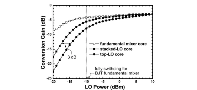
Fig. 4-6 Simulated current conversion gain of the switching core for a fundamental mixer, a stacked-LO mixer and a top-LO mixer core. ... 64
Fig. 4-7 (a) Schematic of the stacked-LO core with LOI at the top cell and LOQ at the bottom cell (b) schematic of the stacked-LO core with LOQ/LOI at top/bottom cells (c) schematic of two stacked-LO cores in parallel. ... 66
Fig. 4-8 Timing diagram of the switching function. Dotted lines represent the switching function without a phase delay, i.e., F1(t) or F2(t). ... 67
Fig. 4-9 (a) Fast Fourier transform (FFT) of the VE at 2fLO with respect to LO voltage (b) FFT of the S(t) at dc and 2fLO with respect to a phase delay for both SHMs. ... 69
Fig. 4-10 Schematic of the SiGe HBT SHMs w/ and w/o delay compensation. (LO bias circuit is not shown for simplicity) ... 71
Fig. 4-11 Die photo of the SiGe HBT SHM w/ compensation. ... 72
Fig. 4-12 Die photo of the SiGe HBT SHM w/o compensation. ... 72
Fig. 4-13 Conversion gain as a function of RF frequency. ... 73
Fig. 4-14 LO-to-RF/IF isolation. ... 73
Fig. 4-15 2LO-to-RF/IF and RF-to-IF isolation. ... 74
Fig. 4-16 Power performance. ... 74
Fig. 4-17 Conversion gain and double sideband noise figure. ... 75
Chapter 5 Fig. 5-1 Block diagrams of dual-conversion receivers (a) with reused second-stage mixer (b) with reused LNA and first-stage mixer (c) with reused first- and second-stage mixers and a switchable mixer RF input stage (d) with reused first- and second-stage mixers. ... 78
Fig. 5-2 Block diagram of a single/dual-band dual-conversion Weaver-Hartley low-IF system. ... 79
Fig. 5-3 Block diagram of the Weaver architecture (a) when input signals are desired RF signal and first image signal (b) when input signals are desired RF signal and second image signal. ... 80 Fig. 5-4 (a)Schematic of a double-quadrature complex mixer topology and its
its complex representation. ... 83 Fig. 5-5 Block diagrams of (a) a double-quadrature-double-quadrature
dual-conversion system and (b) a single-quadrature-double-quadrature dual-conversion system with non-ideal input signals. ... 84 Fig. 5-6 Block diagram of a 0.35-μm SiGe HBT
double-quadrature-double-quadrature Weaver-Hartley low-IF
downconverter. ... 88 Fig. 5-7 (a) Block diagram of a high-precision compensated frequency doubler (b)
schematic of the compensated frequency doubler employed in the LO quadrupler. (Bias circuit is not shown for simplicity) ... 89 Fig. 5-8 Die photo . ... 90 Fig. 5-9 Conversion gain and single-sideband noise figure. ... 91 Fig. 5-10 Power performance. ... 91 Fig. 5-11 IRR of the first/second image signals. ... 91 Fig. 5-12 Output I/Q waveforms. ... 92 Fig. 5-13 Block diagram of a dual-band 0.18-μm CMOS
single-quadrature-double-quadrature Weaver-Hartley low-IF
downconverter. ... 92 Fig. 5-14 (a) Schematic of the LNA with a switchable notch filter and (b) the
simulated frequency response. ... 93 Fig. 5-15 LO1 quadrature signal generator with a two-stage PPF and NMOS switch
pairs. ... 94 Fig. 5-16 Die photo. ... 95 Fig. 5-17 Conversion gain and single-sideband noise figure. ... 95 Fig. 5-18 Power performance. ... 96 Fig. 5-19 IRR of the first/second image signals. ... 96 Fig. 5-20 Input return loss. ... 96 Chapter 6
Fig. 6-1 Schematic of a cascode LNA with a single-to-differential transformer connecting to the transconductance stage of the following I/Q Gilbert mixers. ... 102 Fig. 6-2 Simulated device minimum noise figure (NFmin) at 2.4 GHz and cut-off
frequency (fT) of a 0.18-μm RF NMOS as a function of current density
(JD=ID/W). ... 106
Fig. 6-3 (a) Lg and Ls for power-constrained noise optimization at 2.4 GHz and the
corresponding. The required Lg for different α0 is very similar due to the
cascode LNA without Cp while the supply current is 2.5 mA. The unit for α0 is Ω/nH. ... 108
Fig. 6-4 (a) Cp (b) Lg and Ls for power-constrained simultaneous noise and impedance matching at 2.4 GHz and the corresponding (c) noise figure and (d) voltage gain of the cascode LNA with Cp while the supply current is 2.5 mA. The unit for α0 is Ω/nH. ... 110
Fig. 6-5 (a) Transformer model with a capacitance load C1/C2 at the
primary/secondary coil, respectively (b) schematic of the LNA
transformer with an input varactor and output pure capacitance load. ... 112 Fig. 6-6 (a) Transimpedance gain (ZT) of a transformer as a function of frequency
(b) ZT at a target frequency with respect to X=n2/CR for different
input/output loading capacitance. ... 113 Fig. 6-7 (a) Cross-section view of the vertical-NPN (V-NPN) BJT in deep n-well
0.18-μm COMS process (b) layout of the V-NPN BJTs with four shapes but the same emitter area of 4 μm2. ... 115 Fig. 6-8 (a) Gummel plot (b) current gain (c) current cut-off frequency (d)
maximum oscillation frequency of the V-NPN BJT with four shapes but the same emitter area of 4 μm2. ... 116 Fig. 6-9 Output noise current spectral density of V-NPN BJT and MOS devices.
The dc current is 250 μA for the devices. ... 117 Fig. 6-10 Simulated gm as a function of drain/collector current of both V-NPN
BJT/NMOS transistors. ... 118 Fig. 6-11 VGA with a modified R−r attenuation method. ... 120 Fig. 6-12 (a) numerator (gmRC) and inverse of the denominator [1/(1+gmRE/2)] of
the voltage gain (AV) with different locations of transitions (c) the
corresponding AV as a function of VTIF. ... 120
Fig. 6-13 Block diagram of the 0.18-μm CMOS 2.4-GHz DCR using passive mixers. ... 122 Fig. 6-14 Schematic of (a) single-balanced passive mixer (b) double-balanced
passive mixer with single-ended RF input (c) double-balanced mixer with differential RF input. ... 122 Fig. 6-15 Schematic of a single-stage OP-amp with V-NPN transconductance stage.
... 123 Fig. 6-16 Die photo. ... 124 Fig. 6-17 Conversion gain and double-sideband noise figure. ... 124 Fig. 6-18 Noise figure with respect to IF frequency. ... 125 Fig. 6-19 Conversion gain with respect to IF VGA tuning voltage. ... 125 Fig. 6-20 Output I/Q waveforms. ... 126
Fig. 6-21 I/Q amplitude mismatch and phase error. ... 126 Fig. 6-22 Input return loss. ... 126 Fig. 6-23 LO-to-RF/IF isolation. ... 127 Fig. 6-24 Block diagram of the DCR including LNA, I/Q mixers, I/Q VGAs and an
LO quadrature generator. ... 128 Fig. 6-25 (a) Schematic of the Gilbert mixer with V-NPN BJT in LO switching core
(b) LO switching function with infinite/finite fT in large LO region. ... 129
Fig. 6-26 Conversion gain with respect to LO power at different for different fT
when (a) LO voltage signals are directly fed to the base nodes of the switching core (b) LO signals are generated from a two-stage PPF (c) conversion gain degradation as a function of relative cut-off frequency ( fT fT fLO ). ... 131
Fig. 6-27 (a) Schematic of the two-stage PPF with original capacitive load and additional inductive load (b) calculated optimal voltage division (VD) as a function of inductor quality factor (Q) for different capacitive loadings. ... 135 Fig. 6-28 (a) 3D view and (b) top view of the pseudo-two-turn layout of the fully
symmetric stacked inductor (c) top view and (d) simulated inductance and quality factor of the proposed pseudo-four-turn (equivalent eleven turns) fully symmetric stacked inductor. ... 137 Fig. 6-29 Schematic polyphase loadings including 3D inductor and mixer with
parasitic RB. ... 139
Fig. 6-30 Simulated conversion gain as a function of LO power with different transistor RB. ... 139
Fig. 6-31 Die photo. ... 140 Fig. 6-32 Conversion gain and noise figure with respect to RF frequency. ... 140 Fig. 6-33 Conversion gain as a function of LO power. ... 140 Fig. 6-34 Conversion gain with respect to (a) RF tuning voltage (b) IF tuning
voltage. ... 141 Fig. 6-35 Noise figure with respect to IF frequency. ... 142 Fig. 6-36 Power performance, including IP1dB, IIP3, IIP2. ... 142
Fig. 6-37 (a) I/Q waveforms at RF=2.4 GHz (b) I/Q amplitude imbalance and phase error. ... 143 Fig. 6-38 Block diagram of an I/Q SH-DCR with (a) both quadrature RF and LO
signals (b) differential RF and octet-phase LO signals. ... 145 Fig. 6-39 Top-LO SHM with V-NPN BJTs in LO core. ... 147 Fig. 6-40 Schematic of a multi-stage octet-phase PPF. ... 148 Fig. 6-41 Phasor diagram at (a) second (b) third stage and (c) fourth stage. ... 149
Fig. 6-42 Die photo. ... 151 Fig. 6-43 Conversion gain with respect to LO power. ... 151 Fig. 6-44 Conversion gain with respect to RF frequency. ... 151 Fig. 6-45 Noise figure with respect to IF frequency. ... 152 Fig. 6-46 (a)I/Q waveform at RF=2.4001 GHz, LO=1.2 GHz (b) amplitude
imbalance and phase error. ... 153 Fig. 6-47 Conversion gain with respect to (a) RF tuning voltage (VTRF) (b) IF tuning
voltage (VTIF). ... 154
Fig. 6-48 Power performance (including IP1dB, IIP3 and IIP2). ... 154
Fig. 6-49 (a) LO/2LO-to-RF leakage (b) equivalent output dc offset while the LO power is 8 dBm. ... 155 Fig. 6-50 Block diagram of the I/Q SH-DCR with a tunable narrow-band LNA and a wideband LO generator using 0.18-μm CMOS technology. ... 160 Fig. 6-51 Schematic of an LC tank with a lossy inductor. ... 161 Fig. 6-52 (a)Frequency response of the single/two stage(s) of LC resonator(s) (b) Q
reduction for each tank (c) wideband response with separation of tanks (d) tunable narrow-band response. ... 162 Fig. 6-53 Two-stage LNA with a tunable first-stage LC tank and a tunable
second-stage transformer ... 163 Fig. 6-54 Schematic of the LNA transformer with an input varactor and output pure
capacitance load. ... 165 Fig. 6-55 Top-LO sub-harmonic Gilbert mixer with vertical-NPN BJT in the
switching core while an LC network is applied for an IM2 improvement. ... 166 Fig. 6-56 Block diagram of an LC octet-phase generator including a wideband 45°
phase shifter, cross-coupled buffer amplifiers and single-stage PPF with resonance inductors. ... 168 Fig. 6-57 (a) Schematic of a differential-type wideband 45° phase shifter (b) phase
difference shifter with respect to frequency. ... 169 Fig. 6-58 Cross-coupled differential voltage buffer applied in the LO generator. . 171 Fig. 6-59 Die photo. ... 172 Fig. 6-60 Conversion gain and noise figure with respect to RF frequency. ... 173 Fig. 6-61 Conversion gain with respect to LO power. ... 173 Fig. 6-62 Noise figure with respect to IF frequency. ... 174 Fig. 6-63 Gain difference and phase error of the IF I/Q outputs. ... 174 Fig. 6-64 Conversion gain with respect to (a) RF tuning voltage (VTRF) (b) IF tuning
voltage (VTIF). ... 174
Fig. 6-66 (a) LO/2LO-to-RF isolation (b) Conversion gain when RF=LO+IF and RF=2LO+IF. ... 176 Fig. 6-67 Input return loss. ... 176 Chapter 7
Fig. 7-1 Block diagram of a dual-band double-quadrature-double-quadrature dual-conversion low-IF downconverter. ... 180 Fig. 7-2 Layout extension of the 3D symmetrical inductor. ... 182
List of Tables
Chapter 1
TABLE. 1.1 ISM Band ... 1 TABLE. 1.2 Comparisons for Wireless Personal Area Network ... 3 TABLE. 1.3 High R&D Cost for Deep Submicron CMOS ... 5 Chapter 2
TABLE. 2.1 Performance Comparison of the Gilbert Upconversion Mixers ... 16 TABLE. 2.2 Performance Comparison of the Dual-Band Upconverters
With/Without Bias-Offset TCA ... 25 Chapter 3
TABLE. 3.1 Performance Summary of the 5.7-GHz I/Q Downconverter ... 48 TABLE. 3.2 Performance Summary of the UWB Downconverter Using LR-CR
Quadrature Generator ... 55 Chapter 4
TABLE. 4.1 Performance Comparison of SHMs With Delay Compensation Using Different Technologies ... 76 Chapter 5
TABLE. 5.1 Performance Comparisons of Dual-Conversion Low-IF Receivers .... 98 Chapter 6
TABLE. 6.1 Performance Comparison of DCRs Using Passive Mixers ... 127 TABLE. 6.2 Performance Comparison of DCRs at around 2 GHz ... 144 TABLE. 6.3 Performance Comparisons of SH-DCRs ... 156 TABLE. 6.4 Performance Comparison of Demonstrated 2.4-GHz DCRs ... 158 TABLE. 6.5 Performance Comparisons of SH-DCRs ... 177
List of Abbreviations
BiCMOS Bipolar Complementary Metal Oxide Semiconductor BJT Bipolar Junction Transistor
CG Conversion Gain
DCR Direct-Conversion Receiver
HBT Heterojunction Bipolar Transistor
I/OP1dB Input/Output 1-dB Gain Compression Point
I/OIP3 Input/Output Third-Order Intercept Point
I/OIP2 Input/Output Second-Order Intercept Point
I/Q In-Phase/Quadrature
IRR Image-Rejection Ratio
LO Local Oscillator
NF Noise Figure
PPF Poly-Phase Filter
SH-DCR Sub-Harmonic Direct-Conversion Receiver
SHM Sub-Harmonic Mixer
SiGe Silicon-Germanium
SSB Single Side-Band
TCA Transconductance Amplifier
TIA Transimpedance Amplifier
UWB Ultra-Wideband
VGA Variable-Gain Amplifier
WLAN Wireless Local Area Network WPAN Wireless Personal Area Network
Chapter 1 Introduction
1.1 C
OMMERCIALF
REQUENCYB
ANDS ANDA
PPLICATIONSThe industrial, scientific and medical (ISM) bands and Unlicensed National Information Infrastructure (U-NII) bands are two main unliscensed bands. Thus, they are widely used for wireless communication systems.
The ISM bands were originally reserved internationally for the use of RF energy for industrial, scientific and medical purposes, not for communications. For examples, microwave ovens, and medical diathermy machines. Thus, in general, communication equipments operating in these bands must accept any interference generated by ISM equipments. The ISM bands defined by the International Telecommunication Union Radiocommunication Sector (ITU-R) are listed with the main applications as listed in TABLE. 1.1.
TABLE.1.1ISMBAND
Frequency Band Applications Frequency Band Applications
6.765–6.795 MHz 2.400–2.500 GHz Bluetooth, ZigBee,
WLAN (802.11b/g/n) 13.553–13.567 MHz RFID, NFC 5.725–5.875 GHz HyperLAN, Wi-Fi
26.957–27.283 MHz 24–24.25 GHz
40.66–40.70 MHz 61–61.5 GHz
433.05–434.79 MHz 122–123 GHz
902–928 MHz ZigBee 244–246 GHz
On the other hand, the U-NII band is part of the radio frequency spectrum used by IEEE 802.11a devices and by many wireless internet service providers (ISPs). It operates over the following ranges:
U-NII Low (U-NII-1): 5.15-5.25 GHz.
U-NII Mid (U-NII-2): 5.25-5.35 GHz.
U-NII Worldwide: 5.47-5.725 GHz. Added by Federal Communications Commission (FCC) in 2003.
U-NII Upper (U-NII-3): 5.725-5.825 GHz. Sometimes referred to as U-NII/ISM due to overlap with the ISM band.
Fig. 1-1 shows the comparisons by data rate and distance for different communication technologies, including wireless personal area network (WPAN) and wireless local area network (WLAN). The size of the block represents the costs, i.e., a small block means a lower price. TABLE.1.2 lists the comparisons for popular WPAN systems. The UWB technology has the highest data transmission rate and NFC has the lowest. However, the ZigBee has the longest transceiving distance but relatively low data rate. Based on data rate and transceiving distance of each application, a proper protocol can be chosen. Besides, NFC operates at slower speeds than Bluetooth, but consumes far less power and requires no pairing. NFC sets up faster than standard Bluetooth, but is not much faster than Bluetooth low energy.
TABLE.1.2COMPARISONS FOR WIRELESS PERSONAL AREA NETWORK
WPAN UWB Bluetooth ZigBee NFC Proprietary
Frequency 3.1~10.6 GHz 2.4GHz (ISM) 2.4GHz/898 MHz/915MHz 13.56 MHz Single-/ Dual-Band Distance 0~10m 0~10m 0~75m <50cm 0~75m
Data Rate Very High Low Very Low Very Low Medium
Safety High High Medium Very High High
Price High Medium Low Very Low Low
Standard 802.15.3 802.15.1 802.15.4 IEC
18092/21481
N.A.
As shown in TABLE. 1.2, the proposed low-power transceiver in this dissertation does not focus on any specific standard. Contrarily, long distance, high data rate (for high quality and accurate control) but still low cost are the main goals for implementations. All the proposed techniques and demonstrations are based on these goals. Moreover, a multi-band/multi-standard integration can even be achieved in the future.
1.2 P
ROCESSC
HOSEN1.2.1 Cost vs. Performance
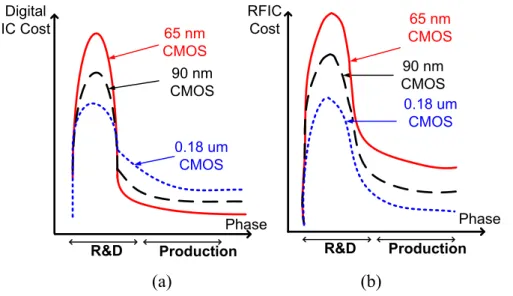
Since the operating frequency of these short-range application is not high (except for the emerging 60-GHz high-data-rate application), various technologies can be chosen to achieve required functions and specifications. Fig. 1-2 shows the technology development in TSMC. The 28nm logic circuits are now available but the mixed-signal/radio-frequency (MS/RF) circuits are still developing. On the other hand, the 40 nm process is available for MS/RF circuits. However, 0.18-μm CMOS is still the mainstream technology.
product is entering mass production, the barrier for research and development (R&D) makes it very hard to finish a final product. The concept of the barrier for the CMOS R&D cost for digital and RF ICs is illustrated in Fig. 1-3(a) and (b), respectively. The Y-axis is the cost and the X-axis is the production phase. Fig. 1-3(a) shows the cost reduction of the digital circuit as CMOS scaling although the R&D cost is high. It is noteworthy that Fig. 1-3(a) is similar to a conventional diagram of the activation energy. TABLE. 1.3 also lists the R&D cost of every technology, pronounced by Chang, ISSCC 2007.
*0.13 μm embedded flash is actually shrunk to 0.11 μm
Fig. 1-2 TSMC Technology Development
R&D Production Phase 65 nm CMOS 0.18 um CMOS 90 nm CMOS Digital IC Cost CMOS65 nm 90 nm CMOS R&D Phase Production RFIC Cost 0.18 um CMOS (a) (b)
TABLE.1.3R&DCOST FOR DEEP SUBMICRON CMOS
Technology Cost (Wafer/Mask set)
0.18 um 1.4K/120K
0.13 um 1.8K/300K
90 nm 2.5K/900K
65 nm 3.8K/1400K
On the other hand, because the operating frequency is relatively low, the passive components limit the size reduction. This is the biggest difference from the digital circuits, as shown in Fig. 1-3 (b). Thus, choosing a proper, not always the most advanced, technology can save significant cost.
1.2.2 Flicker Noise
However, a CMOS process has severe flicker noise problems. The dangling bonds, appearing at the interface between the gate oxide and the silicon substrate in a MOSFET, give rise to extra energy states. Thus, when charge carriers move at the interface, some are randomly trapped and later released by such energy states, introducing the flicker noise in the drain current. Typically, the noise spectral density of the flicker noise is inverse proportional to frequency and thus the flicker noise is also called 1/f noise.
In this dissertation, various solutions for flicker noise problems are provided. Direct-conversion receivers (DCRs) with fundamnetal mixer (in Chapter 3) or sub-harmonic mixers (in Chapter 4) are demonstrate using silicon germanium (SiGe) heterojunction bipolar transistor (HBT) technology for good gain/noise performance and flicker noise free property at a higher cost. A low-IF architecutre with IF frequency set over the flicker noise corner (discussed in Chapter 5) is another straightforward flicker noise solution. However, a higher power consumption is
required for both RF and analog to digital converter (ADC) circuits. On the other hand, the parasitic deep-n-well (DNW) bipolar junction transistor (BJT), which has an ultra-low flicker noise, is available in standard CMOS process without extra cost. However, the low transistor cut-off freuqency (fT) of the parasitic BJT devices
becomes another challenge for designers and is deeply analysis and then solved in Chapter 6.
Chapter 2 High Linearity Gilbert Upconversion
Mixer
2.1 H
IGH-L
INEARITYB
IAS-O
FFSETTCA
2.1.1 Introduction
Linearity is an important issue in communication systems, especially in transmitters. The passive mixers, e.g., the resistive mixers [1] or the diode mixers [2], are demonstrated with high linearity but severe loss. On the other hand, a Gilbert mixer topology is widely used in a wireless transceiver to avoid the severe loss at high frequencies. However, a conventional Gilbert mixer with emitter-coupled (source-coupled) differential pair input stage suffers from a poor linearity and therefore the signals of adjacent channels easily interfere with the desired channel. Note that, a differential topology, either with a tail current source at low frequency or an parallel LC tank at high frequencies, has a better common-mode rejection and also a higher second-order input-referred intercept point (IIP2).
V1 V2
Io1 Io2
(a) (b) (c)
Fig. 2-1 (a) BJT differential amplifier (b) MOS differential amplifier (c) MOS pseudo-differential pair.
The transfer function of a BJT differential pair with an ideal current source, as
shown in Fig. 2-1(a), is tanh( )
2 id c T v i V
[3], which is obtained from the I-V
On the other hand, the transfer function of a MOS differential pair [ in Fig. 2-1(b)] is 2 2 3 3 2 ( ) 1 1 ( ) 1 ( ) 8 ( ) 8 id d id OV OV id id OV OV id id OV OV v I i v V V v I v V V I I v v V V (2.1)
and the third order term cannot be omitted [4] even without considering the short-channel effect. The MOS pseudo-differential topology [ in Fig. 2-1(c)] has much better IIP3 but a worse IIP2.
Many ideas are utilized to improve linearity. For example, a multi-tanh approach [5] and a class-AB transconductance [6] are designed to provide more linear transfer function of the transconductor by eliminating high order terms of the exponential function of bipolar junction transistors (BJTs) or the short channel effect of the MOS transistors. A feedback technique is also widely employed by strongly suppressing the high-order distortion at the cost of gain [7], e.g., emitter (source) degeneration.
Fig. 2-2 Block diagram of the single-/dual-band Gilbert upconverter.
The block diagram of a single-/dual-band Gilbert upconversion mixer is illustrated in Fig. 2-2. A Gilbert mixer core is employed to commutate IIF with LO
frequency to produce IRF while IIF is generated by a transconductance amplifier (TCA)
current combiner with extra gain improvement [8] and then a transimpedance amplifier (TIA) translates the output current (IRF) to the voltage signal (VRF) and
achieves output matching simultaneously.
The current commutation is a highly linear process and only translates the IF signal to the RF signal with every odd order LO frequencies. Besides, the passive resonator is inherently linear. Consequently, the input TCA and output TIA play important roles for the linearity issue.
Fig. 2-3 Bias-offset transconductance amplifier.
In this chapter, a bias-offset cross-coupled TCA [9] is employed at the IF port for linearity improvement. The TCA consists of two differential pairs with a constant bias offset (VB), as shown in Fig. 2-3. The transconductance (gm) of the TCA is derived as
follows, assuming all transistors are in a square-law region.
2 2 1 1 4 1 4 2 2 2 2 3 2 3 ( ) ( ) ( ) ( ) o M M IF x Tn IF B x Tn o M M IF x Tn IF B x Tn i i i k V V V k V V V V i i i k V V V k V V V V , (2.2) where 1 , 1, 2,3, 4 1 2, 3 4 2 i i n ox i W k C i k k k k L
and VB is the gate-to-source voltage
drop of M5-M6 which provides a constant dc offset voltage for the two differential
1 2 1 3 ( )( 2 2 ) ( )( 2 2 2 ) o o IF IF IF IF x tn IF IF IF IF x Tn B i i k V V V V V V k V V V V V V V (2.3) because 2VIFVIF= VCMis a constant dc,
1 2 ( ) 2 1 3)( 2 3 o o IF IF CM x Tn B i i V V ( -k k V V V )+ k V . (2.4) Thus, gm 2kV if k kB, 1 k3 . The gm is a constant and no third-orderinter-modulation occurs ideally. However, the short-channel effect degrades the linearity, especially when a large gate-to-source voltage is applied on the device with a shorter gate length in an advanced CMOS technology.
Gilbert upconversion mixers with NMOS/PMOS bias-offset TCAs are implemented, respectively, and fully compared in next section.
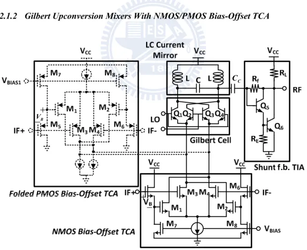
2.1.2 Gilbert Upconversion Mixers With NMOS/PMOS Bias-Offset TCA
B V C C
Fig. 2-4 Schematic of the Gilbert upconverters with NMOS/PMOS-type bias-offset TCAs and a single-band LC current combiner.
The schematics of the Gilbert upconversion mixers with NMOS-type and folded PMOS-type input stages are shown in Fig. 2-4. The bias-offset differential pair employed in the input stage has the transconductance of 2kVB if the MOS
characteristic is still in a square-law region with a long channel transfer function, as introduced in Section 2.1.1.
The NMOS and PMOS I-V characteristics are shown in Fig. 2-5(a) and (b) with the gate lengths of 0.5 μm, 1 μm, and 2 μm and the correspondent widths of 25 μm, 50 μm, and 100 μm, respectively. 0.0 0.5 1.0 1.5 2.0 2.5 0.0 0.5 1.0 1.5 2.0 2.5 3.0 3.5 4.0 4.5 5.0 short channel W/L= 100u/ 2u W/L= 50u/ 1u W/L= 25u/ 0.5u Vgs=0.8V Vgs=1.0V Vgs=1.2V Vgs=1.4V Vgs=1.6V I ds (m A ) Vds (V) long channel (a) 0.0 0.5 1.0 1.5 2.0 2.5 0.0 0.2 0.4 0.6 0.8 1.0 1.2 1.4 1.6 1.8 2.0 Vsg=1.2V Vsg=1.0V Vsg=1.4V Vsg=1.6V Vsg=1.8V W/L= 100u/ 2u W/L= 50u/ 1u W/L= 25u/0.5u I sd (m A) Vsd (V) Vsg=2.0V Vsg-|Vt| (b)
The drain saturation voltage, Vdsat, is less than the gate-overdrive voltage,
Vgs−VT=VOV, if the short channel effect takes place. However, if VOV is still small, the transistors are still in the long channel region because the electric field is not large enough to saturate the velocity of the electrons as depicted in Fig. 2-5(a). Contrarily, the PMOS is almost in the long channel region even if the gate-overdrive voltage is large as shown in Fig. 2-5(b). Moreover, if the device is still in the long channel region, the drain saturation currents are almost the same if the W/L ratio is kept at a constant as shown in Fig. 2-5(b). On the other hand, the saturation current of a short channel device is lower than that of the long channel device when the W/L ratio is kept the same as shown in Fig. 2-5(a). In addition, a shorter gate length results in a smaller output resistance of the MOS transistor.
The gate length of the NMOS transistors, M1-M4, in the input stage of the first
chip is 0.5 μm while the gate length of the PMOS transistors, M1-M4, of the other chip
is 1μm. For the lower mobility of PMOS transistors, the widths of the PMOS transistors are designed much wider to achieve similar transconductance gain when compared to the upconverter with the NMOS TCA. As a result, the IF bandwidth of the upconverter with the PMOS TCA is much narrower than that with the NMOS TCA.
Instead of using the MOS transistors in the Gilbert switching quad with a large LO switching voltage requirement of 2VOV(gate-overdrive voltage), the bipolar transistors Q1-Q4 are utilized in this work with only about 0.1-V LO voltage swing
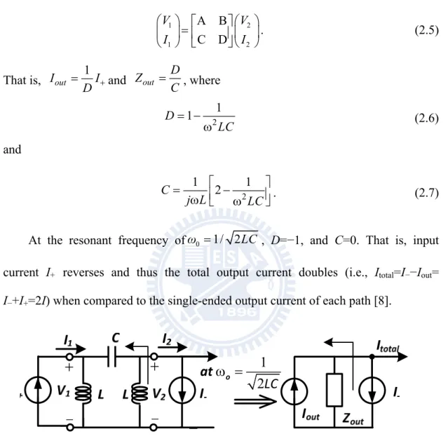
requirement to make the current fully switch. The current commutation mechanism is highly linear and only performs the frequency translation. A single band current combiner with a π-shape is shown in Fig. 2-6 with the differential input current I+ and
represented by its Norton equivalence Iout and Zout as shown in Fig. 2-6. The
equivalent current source (Iout) and the output equivalent impedance (Zout) can be
obtained by of the ABCD matrix
1 2 1 2 A B C D V V I I . (2.5) That is, Iout 1 I
D and Zout D C , where 2 1 1 D LC (2.6) and 2 1 1 2 C j L LC . (2.7) At the resonant frequency ofω0 1/ 2LC , D=−1, and C=0. That is, input current I+ reverses and thus the total output current doubles (i.e., Itotal=I−−Iout=
I−+I+=2I) when compared to the single-ended output current of each path [8].
1
2
LC
oat
Fig. 2-6 Block diagram of the LC current combiner and its equivalent circuit at the resonant frequency.
The output shunt-shunt feedback TIA is employed to translate the combined current output Itot to the voltage signal. Moreover, the output impedance is reduced by the factor of (1+A for the shunt-type feedback and thus the output matching is easily achieved. The 20-GHz bandwidth of the feedback TIA is designed with strong feedback to reduce the nonlinearity effect.
utilizing NMOS and PMOS TCAs are shown in Fig. 2-7(a) and (b), respectively. On-wafer measurement facilitates the RF performance.
(a) (b)
Fig. 2-7 Die photo of the Gilbert upconverter (a) using an NMOS TCA (b) using a PMOS TCA.
3.0 3.5 4.0 4.5 5.0 5.5 6.0 6.5 -20 -18 -16 -14 -12 -10 -8 -6 -4 -2 0 Co n ver sio n Gai n (d B) RF frequency(GHz) NMOS PMOS Fixed IF =20 MHz
Fig. 2-8 Conversion gain with respect to RF frequency.
The peak conversion gain of the upconverters with NMOS/PMOS input TCAs occurs at both RF=4.4 GHz, IF=20 MHz and the LO power is −5 dBm as shown in Fig. 2-8. The power performance of the upconverters with NMOS/PMOS TCAs is shown in Fig. 2-9. The OP1dB and OIP3 are −11/−11 dBm and 5.5/9.5 dBm for the
-30 -25 -20 -15 -10 -5 0 5 10 15 20 -80 -70 -60 -50 -40 -30 -20 -10 0 10 20 OIP3=5.5 dBm OIP3=9.5 dBm OP1dB=-11 dBm Ou tp ut Po wer (dBm) IF power(dBm) Pout(f1) @ RF=4.4GHz Pout(2f1-f2) @ RF=4.4GHz tone spacing=1MHz
Fig. 2-9 Power performance.
1 10 100 1000 -20 -18 -16 -14 -12 -10 -8 -6 -4 -2 0 f3dB=100 MHz Co nver sio n Gain (d B) IF Frequency(MHz) NMOS PMOS Fixed RF=4.5GHz f3dB=500 MHz Fig. 2-10 IF bandwidth. 4.0 4.2 4.4 4.6 4.8 5.0 5.2 0 10 20 30 40 50 Isolation (d B) LO Frequency (GHz) NMOS PMOS LO-to-RF Isolation
The IF bandwidth of the upconverters with NMOS and PMOS TCAs are 500 MHz and 100 MHz, respectively, as shown in Fig. 2-10. The upconverter with a PMOS TCA has a 20.5-dB difference between the OIP3 and OP1dB which is larger
than a 16.5-dB difference for the upconverter with an NMOS TCA at the cost of a narrower IF bandwidth for a similar gain design purpose. However, both designs are much more linear than a conventional Gilbert upconverter. The output RF return loss is better than 16 dB for both circuits over 20 GHz. The LO-to-RF isolation of each upconverter is better than 28/26 dB when LO frequency ranging from 4-5.2 GHz as shown in Fig. 2-11. The power consumption of each circuit is 40/46 mW, respectively. TABLE. 2.1 compares the proposed high-linearity Gilbert upconversion mixers using NMOS/PMOS TCA to the state-of-the-art circuits in literatures [8], [10]-[12].
TABLE.2.1PERFORMANCE COMPARISON OF THE GILBERT UPCONVERSION MIXERS
w/ NMOS TCA w/ PMOS TCA [8] [10] [11] [12] RF (GHz) 4.4 4.4 5.2 5.8 5.8 5.2 Gain (dB) −4 −6 1 −2.9 −2.9 −1 LO-to-RF Isolation (dB) 28 26 38 NR NR 39 OP1dB (dBm) −11 −11 −10 −3.4 −3.4 −10 OIP3(dBm) 5.5 9.5 2 4.6 4.6 6 Supply Voltage (V) 3.5 3.3 5 VEE= −2.7 VEE= −2.7 3.3 Power Consumption (mW) 40 46 32.5 40.5 40.5 37.95 Technology 0.35m SiGe HBT 0.35m SiGe HBT 2m GaInP/GaAs HBT 0.8m SiGe HBT 0.8m SiGe HBT 0.35m SiGe HBT
2.2 D
UAL-B
ANDH
IGH-L
INEARITYG
ILBERTU
PCONVERSIONM
IXER2.2.1 Dual-Band LC Current Combiner
For wireless communication systems, the current trend is toward multi-standards/multi-services, and thus it brings multi-band circuit design on a single chip, especially for dual-band (wireless local area network) WLAN applications [13]-[16]. Traditionally, it can be procured by using a dual-band filter cascaded after RF output stage at the cost of extra loss. However, in this section, a dual-band LC current combiner is introduced and applied at the load of the Gilbert upconversion mixers for a 2.4/5.7 GHz dual-band operation.
Fig. 2-12 Operational principle of the dual-band LC current combiner.
2
2 2ω
2 1ω
2 Dω
2 Dω
2 Cω
ph1L
sC
ph2L
pC
C
p sL
Low Bandpass High Bandpass
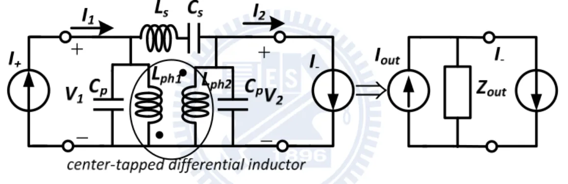
A single-band LC current combiner is introduced in Section 2.1.2. The dual-band version of the π-shaped LC current combiner is illustrated in Fig. 2-12. At low frequencies, the series branch is dominated by 1/j C S while the shunt branch is
dominated by 1 /j LPh1,2. On the other hand, the series and shunt branches are
dominated by j L S and j C P at high frequencies, respectively. Therefore, the
π-shaped dual-band LC current combiner can be treated implicitly as a combination of a low-frequency band-pass (LPh1, LPh2, and CS) resonator and a high-frequency band-pass (LS, CP) resonator as shown in Fig. 2-13.
Using the same method applied to a single-band LC current combiner, the target frequency of current reversion can be obtained by letting D=−1,
where
1 2 2 2 1 0 1 1 S P P S P S S P V L I C D C L I L C C L . (2.8)At that frequency, Itotal=I−−Iout= I−+I+=2I and ideally 6 dB gain improvement is
obtained when compared to each output node of the Gilbert mixer. When the element D of the ABCD matrix equals −1, i.e.,
4 2 2 1 0
P P S S P P S S P S
L C L C L C L C L C
. (2.9)
Iout=I+ is achieved, and therefore the equivalent total output current doubles. The roots
of Eqn. (2.9) are and1 , which can be found as 2
2 2 C D (2.10) where 2 2 2 1 2 ( 2 ) 2 2 P P S S P S C P P S S L C L C L C L C L C (2.11) and
2 2 2 2 2 1 ( 2 ) 4 2 2 P P S S P S P P S S D P P S S L C L C L C L C L C L C L C . (2.12)
The design procedure of the dual-band LC current combiner is as follows: a) Define the dual-band frequencies1and2. Thus the center frequencyCand
difference frequency D are specified by Eqns. (2.11) and (2.12).
b) Choose proper inductors (LS and LP) with high qualify factors at the desired
frequencies.
c) Calculate the value of CS and CP by knownCandD.
For the application on WLAN 802.11a/g, the two frequencies are specified as f1=
2.4 GHz and f2=5.7 GHz, respectively. The series capacitor CS is decomposed into
two capacitors with capacitance of 2CS and these two capacitors are connected to each
end of the floating inductor LS for fully symmetric layout design. The lower limitation
of inductances LS and LP are constraint by the achievable fQmax in practice while the
capacitances of CS and CP are restricted by the severe parasitic effects. Consequently,
2CS=0.8 pF and CP=1 pF and the inductances of LP and LS are 1.85 nH and 4.6 nH,
respectively. In the dual-band LC current combiner, a 5-square-turn symmetric inductor (LS) is 3 μm line width, 3 μm line spacing and outer diameter of 120 μm
while a center-tapped symmetric differential inductor, LP (consisting of LPh1 and LPh2), is composed of a 5-square-turn with line width, spacing and outer diameter of 4, 2.5, and 120 μm, respectively. In real implementation of on-chip inductors, the output impedance of the dual-band resonator at resonance frequency of 2.4 GHz and 5.7 GHz are both 120 Ω, by Agilent Advanced Design System (ADS) simulation.
The following sections introduce two implementations using the proposed dual-band current combiner. Section 2.2.2 describes a dual-band upconverter with a conventional BJT differential amplifier as an input TCA while a bias-offset TCA
introduced in Section 2.1.1 is further applied in the dual-band upconverter with linearity improvement in Section 2.2.3.
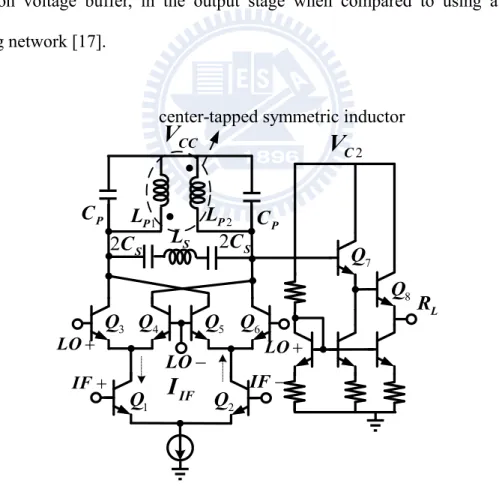
2.2.2 Dual-Band Upconversion Mixer With a Dual-Band LC Current Combiner
The schematic of the 2.4/5.7-GHz dual-band Gilbert upconverter using 0.35-μm SiGe HBT technology is shown in Fig. 2-14. The proposed dual-band LC current combiner is applied at the output of the Gilbert mixer. The chosen of inductance, capacitance and the real geometric size of real implementations in the dual-band current combiner are introduced in Section 2.2.1. Moreover, the power improvement of the Gilbert upconverter is achieved by using the active matching network, the Darlington voltage buffer, in the output stage when compared to using a passive matching network [17]. IF IF 2 C
V
LR
1Q
Q
2 3Q
Q
4Q
6 7Q
8Q
5Q
CCV
2 PL
2
C
SL
S2
C
S 1 PL
PC
PC
center-tapped symmetric inductor
LO LO LO IF
I
Fig. 2-14 Schematic of the 2.4/5.7 GHz Gilbert upconverter with a dual-band LC current combiner.
The die photo of the dual-band upconverter is shown in Fig. 2-15 and the die size is 1×1 mm2.
Fig. 2-15 Die photo. 1.5 2.0 2.5 3.0 3.5 4.0 4.5 5.0 5.5 6.0 6.5 7.0 7.5 -25 -20 -15 -10 -5 0 5 Co n ver sio n Gain (d B) RF frequency (GHz) Conversion Gain Fixed IF=100 MHz
Fig. 2-16 Conversion gain with respect to RF frequency.
-30 -25 -20 -15 -10 -5 0 5 -80 -70 -60 -50 -40 -30 -20 -10 0 10 IP1dB=-11 dBm IIP3=1 dBm IP1dB=-11.5 dBm Pout(f1) @RF=2.4GHz Pout(2f1-f2) @RF=2.4GHz Pout(f1) @RF=5.7GHz Pout(2f1-f2) @RF=5.7GHz RF power (dBm) IF power (dBm) IIP3=0.5 dBm
Fig. 2-16 shows the conversion gain with respect to RF output frequency when
IF=100 MHz. The measured conversion gain at desired frequencies of 2.4/5.7 GHz is
−3/−3.5 dB with the LO input power of −4 dBm. However, the peak conversion gain is 0/−3 dB at 2.7/5.9 GHz due to the process variation. As shown in Fig. 2-17, the dual-band upconverter has the IP1dB of −11.5/−11 dBm, and the IIP3 of 0.5/1 dBm
when IF=100 MHz, RF=2.4 GHz and 5.7 GHz, respectively. The power consumption is 49.5 mW at a 3.3-V supply.
2.2.3 2.4/5.7 GHz High-Linearity Gilbert Upconversion Mixer
The schematic of the 2.4/5.7 GHz dual-band SiGe BiCMOS Gilbert upconversion mixer is shown in Fig. 2-18. The upconverter in Fig. 2-18 consists of a SiGe HBT LO Gilbert mixer core (Q1-Q4), an IF bias-offset CMOS TCA (M1-M4),
and an RF output dual-band LC current combiner with a SiGe HBT TIA output buffer (Q5-Q6). S L RF
Fig. 2-18 Schematic of the SiGe BiCMOS dual-band Gilbert upconverter with the bias-offset TCA and dual-band LC current combiner.
As mentioned in Section 2.1.1, the transconductance of the TCA equals to 2kVB as long as the NMOS I-V characteristics is in the square-law long channel region. The NMOS devices M1-M4 are biased at a small gate overdrive voltage and the gate
lengths of the MOS transistors are 0.5 μm to mitigate the short channel effect. A shunt-shunt feedback TIA is employed in the output stage to achieve output matching. A wideband TIA with a 3dB bandwidth of 20 GHz is designed because strong feedback results in high linearity improvement. Passive matching output network is another choice [18].
The SiGe BiCMOS 2.4/5.7 GHz dual-band upconverter facilitates on-wafer rf measurements. Fig. 2-19 shows the die photo of the dual-band upconverter and the die size is 1.13×0.97 mm2. The supply voltage is 3.5 V and the current consumption of the mixer core with the common-drain-configured M5 and M6 input buffers is 6.95
mA.
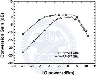
Fig. 2-19 Die photo.
In Fig. 2-20, the measured peak conversion gain at 2.4 GHz and 5.7 GHz is 1.5 and −0.2 dB, respectively, with 3dB bandwidth of 750 MHz when LO power is −5 dBm.
Fig. 2-20 Conversion gain as a function of RF frequency. -30 -25 -20 -15 -10 -5 0 5 10 15 -30 -25 -20 -15 -10 -5 0 5 10 C o n ver sion Gain (dB ) LO power (dBm) RF=2.4 GHz RF=5.7 GHz
Fig. 2-21 Conversion gain with respect to LO power at RF=2.4 and 5.7 GHz.
The measured conversion gain varies within 1 dB when LO power changes from –12 dBm to 4 dBm with RF=2.4 GHz, LO=2.3 GHz and IF=100 MHz while it changes from −6 dBm to 5 dBm with RF=5.7 GHz, LO=5.6 GHz and IF=100 MHz, as shown in Fig. 2-21. The output RF return loss is better than 13 dB at both 2.4/5.7 GHz. The power performance of the dual-band upconverter is illustrated in Fig. 2-22. It has OP1dB of −10.5/−9 dBm, and OIP3 of 12/13 dBm when input IF=100 MHz,
RF=2.4 GHz and 5.7 GHz respectively. The measured LO-to-RF isolation is 38/43 dB when LO=2.3 GHz and 5.6 GHz, respectively. The difference between OIP3 and
OP1dB can be used to indicate the linearity and our work shows excellent linearity of
22 dB difference between OIP3 and OP1dB.
TABLE. 2.2 summarizes the comparison of the proposed Gilbert upconversion mixer using bias-offset TCA in this section and that using conventional BJT differential pair introduced in Section 2.2.2. It is obvious that the difference between OIP3 and OP1dB is improved by around 9 dB when using a bias-offset TCA to replace
the conventional BJT differential pair.
TABLE.2.2PERFORMANCE COMPARISON OF THE DUAL-BAND UPCONVERTERS
WITH/WITHOUT BIAS-OFFSET TCA
w/ Bias-Offset TCA w/ BJT Differential Pair TCA
RF (GHz) 2.4/5.7 2.4/5.7 Gain (dB) 1.5/−0.2 −3/−3.5 LO-to-RF Isolation (dB) 38/43 30/32 OP1dB (dBm) −10.5/−9 −15.5/−15.5 OIP3 (dBm) 12/13 −2.5/−2.5 Supply Voltage (V) 3.5 3.3 Power Consumption (mW) 45 49.5
Chapter 3 Passive Quadrature Signal
Generations and Their Applications on BJT-
based Gilbert Mixers
3.1 P
ASSIVEQ
UADRATURES
IGNALG
ENERATIONA quadrature signal generation with accurate amplitude and phase is always an important issue for communication systems, e.g., quadrature up/down conversion mixers [19] and sub-harmonic mixers (SHMs) [20], because the quadrature accuracy determines the bit-error rate (BER) performance.
Typically, there are four main methods for generating quadrature signals: 1) A frequency divider,
2) a quadrature voltage-controlled oscillator (QVCO),
3) distributed elements, e.g., a quarter-wavelength coupler or a branch-line coupler, 4) lumped elements, e.g., an RC-CR, LR-CR phase shifter and even a poly-phase
filter (PPF).
An even-modulus divider, e.g., a divide-by-two divider, can generate accurate quadrature signals but it requires an input signal with twice the RF frequency and an extra dc power consumption. However, its wideband performance and excellent accuracy are very attractive and thus is widely used in real applications [14], [21]. On the other hand, a QVCO suffers from a strong trade-offs between quadrature phase accuracy and phase noise performance. Thus, it is difficult to achieve both of them at the same time [22]-[24]. A passive coupler has an advantage over the lumped circuits especially at high frequencies; however, it occupies a bulky area at low frequencies [25], e.g., below 10 GHz. Passive realizations using either distributed or lumped components have unavoidable power loss. However, when applying to low-frequency