國
立
交
通
大
學
電子工程學系 電子研究所
博 士 論 文
用於頻率合成器及無線通訊之金氧半積體電路技術
CMOS CIRCUIT TECHNIQUES FOR FREQUENCY
SYNTHESIS AND WIRELESS COMMUNICATION
研 究 生:盧台祐
(Tai-You Lu)
指導教授:陳巍仁
(Wei-Zen Chen)
用於頻率合成器及無線通訊之金氧半積體電路技術
CMOS CIRCUIT TECHNIQUES FOR FREQUENCY
SYNTHESIS AND WIRELESS COMMUNICATION
研 究 生
:盧台祐
Student: Tai-You Lu
指導教授:陳巍仁
Advisor: Wei-Zen Chen
國 立 交 通 大 學
電子工程學系 電子研究所
博 士 論 文
A Dissertation
Submitted to Department of Electronics Engineering &
Institute of Electronics
College of Electrical and Computer Engineering
National Chiao Tung University
in Partial Fulfillment of the Requirements
for the Degree of
Doctor of Philosophy
in
Electronics Engineering
July 2011
Hsinchu, Taiwan, Republic of China
研究生:盧台祐
指導教授:陳巍仁 博士
國立交通大學電子工程學系電子研究所
摘要
隨著通訊系統及互補式金氧半導體之快速發展,應用於當代無線通訊系統之收發 器電路技巧仍然是被迫切需要。頻率合成技巧是一項在收發器裡面不可或缺的技術,主
要是用來執行產生穩定且低雜訊之本地振盪信號(Local oscillator, LO),或是用於直接調
變(Direct modulation)傳送。這些頻率合成器必需要符合低成本、低功率及低電壓操作之 單晶片設計,並且也要能滿足相位雜訊及切換速度之系統規格。於各式各樣的通訊系統 中,頻率合成器將面對不同的挑戰需要去克服。一訊號源操作於sub-THz(0.1-1 THz)頻 率範圍被需要應用於感測、進階影像及生化偵測等應用。同時,射頻電路也被嘗試數位 化並與基頻電路整合。對於生活的品質來說,一個低尺寸(form factor)及低功率之收發 器則被需要用於生醫電子。 有鑒於此,本論文將開發金氧半電路技巧於頻率合成技術與無線通訊系統去克服 將面臨的挑戰。發展數位輔助之射頻電路而應用於sub-THz 影像系統與無線個人區域網 路。除此之外,一高整合度之無線收發器也完成於無線身體區域網路而讓其應用能更普 及。主要的研究主題有四項,其包括:(1)設計與分析一個數位控制且可切換模式之駐 波振盪器,能產生基頻與三倍頻信號於sub-THz 頻帶; (2)設計與分析具數位可重組傳輸
線之寬調節範圍數位控制振盪器(Digitally controlled oscillator, DCO)於無線高畫質傳輸;
合成器; (4)一無參考信號源(reference-less)且具 1 Mbps QPSK 調變之單晶片無線接收器 應用於無線身體感測網路。 本論文第二章首先探討各種頻率合成技術並探究其特點。直接、間接及數位頻率 合成技巧將被介紹並總結其特點於此章節。 第 三 章 , 介 紹 電 感 電 容 共 振 腔 式 電 壓 控 制 振 盪 器(LC-tank voltage-controlled oscillator)之設計考量。接下來,提出一個 38/114 GHz 可切換模式且能同步鎖定之駐波
振盪器(Standing wave oscillator, SWO)。三倍頻之輸出頻率可以被數位控制激發以操作
於不同模式。實驗模型以低漏電65 nm 互補式金氧半導體技術製造。結合同步鎖定技巧, 於 38 GHz 偏移 1 MHz 頻率所量測之相位雜訊在鎖定前後分別為-102 dBc/Hz 與-120 dBc/Hz。在模式 1 操作於 38 GHz 及模式 3 操作於 114 GHz 下,所消耗之功率於 1.2 V 之偏壓下分別為4 mA 及 20 mA,其晶片面積為 720×880 μm2. 第四章,介紹電感電容共振腔式數位控制振盪器之設計考量。之後,設計完成一 具75 kHz 解析度之 10 GHz 電感電容共振腔式數位控制振盪器應用於全數位鎖相迴路。 其更精細之頻率解析度可進一步藉由高速之合差調變器(ΔΣ modulator)達成。所量測於 1 MHz 偏移頻率之相位雜訊為-102 dBc/Hz,使用 90 nm 互補式金氧半導體技術製造其共 消耗3.9 mW 於 1 V 之偏壓下。除此之外,一使用線性可變電感之 40 GHz 且具 14%調 節範圍之數位控制放大器應用於60 GHz 超寬頻系統也被介紹於此。藉著所提出之技術, 寬調節範圍及多頻帶操作可以被完成而不犧牲其振盪頻率。使用90 nm 數位互補式金氧 半導體技術,其能涵蓋38.6 GHz 至 43.4 GHz 之操作頻率。自 43 GHz 所量測 10 MHz 偏移頻率之相位雜訊為-109 dBc/Hz,輸出功率為-11 dBm。此數位控制振盪器於 1.2 V 偏壓下共消耗19 mW。晶片面積為 0.5 × 0.15 mm2。 第五章提出一使用直接頻率合成技巧之 3 至 10 GHz、14 個頻帶且具突波(Spurs) 縮減之頻率合成器應用於多頻帶超寬頻正交多頻分工系統。基於單一個鎖相迴路及兩級
混頻之架構,其能降低諧波混合(Harmonic mixing)與頻率拉扯(Frequency pulling)之效應
以抑制突波產生。同時,於鎖相迴路之迴授路徑上也只需要除二除頻器。因此更精準之
正交次諧波項 (I/Q sub-harmonics) 能夠被單旁波帶混波器(Single sideband mixer, SSB
mixer)利用以產生 14 個載波頻率。經實驗結果,於正交信號校正後,鏡像突波(Image spur)
可以被改善 22dB 且抑制至-45 dBc 以下。使用 0.18 μm 互補式金氧半導體技術製造,
位調變(QPSK modulation) ,使用 0.18 μm 互補式金氧半導體技術製造。此接收器直接 由接收的射頻信號中,完成本地振盪載波之回復與資料解調變,而不需要振盪器形式之
參考源及額外之類比至數位信號轉換器(Analog to digital converter, ADC)於基頻。其整合
低雜訊放大器(Low noise amplifier, LNA)、混頻器、本地振盪載波回復迴路(LO recovery
loop)、後級放大器(Post amplifier)及數位解調變器(Digital demodulator)於單一晶片,於 1.8 V 電壓供應下共消耗 20.4 mW。由回復之載波於 2.432 GHz 所量測到 1 MHz 偏移頻
率之相位雜訊為-112 dBc/Hz。晶片面積為 1.75 x 1.55 mm2。
CMOS CIRCUIT TECHNIQUES FOR FREQUENCY
SYNTHESIS AND WIRELESS COMMUNICATION
Student: Tai-You Lu Advisor: Dr. Wei-Zen Chen
Department of Electronics Engineering and Institute of Electronics
National Chiao-Tung University
Abstract
With the rapid development of communication system and CMOS technology, the circuit techniques of contemporary transceivers for wireless communication remain to be imperatively desired. The frequency synthesis technique is an essential technique in transceivers to perform a stable and high purity local oscillator (LO) generation, or direct modulation transmission. These synthesizers need to meet the stringent requirements of low cost, low power and low voltage monolithic implementation while also meeting the phase noise and switching transient specifications. For various communication systems, the frequency synthesizers have to face different challenges that need to be overcome. The signal source at sub-THz (0.1-1 THz) is required for sensing, advanced imaging or bio-agent chemical detection application. Also, the RF circuits are tried to be digitalized and to be integrated with baseband. For quality of life, a small form factor and low power transceiver is needed for healthy electronics.
This dissertation develops the CMOS circuit techniques for frequency synthesis and wireless communications to conquer the encountered challenges. The digital assisted RF techniques are developed for sub-THz imaging system and wireless personal area network. Besides, a highly integrated wireless transceiver for wireless body area network is achieved to promote pervasive adaptations. There are four major topics in this dissertation, including: (1) the design and analysis of a digitally controlled switched-mode standing wave oscillator
design and analysis of wide tuning range digitally controlled oscillators with digitally reconfigurable transmission line for wireless high definition; (3) a fast hopping MB-OFDM UWB (multi-band orthogonal frequency division multiplexing) frequency synthesizer with digital I/Q calibration for spurs reduction; (4) a reference-less single chip wireless receiver for 1 Mbps QPSK demodulation applied in wireless body sensor network.
Chapter 2 reviews various types of frequency synthesis techniques and explores their characteristics. The direct, indirect and digital frequency synthesis are introduced and summarized in this chapter.
In chapter 3, the design considerations of a LC-type voltage controlled oscillator (VCO) are introduced. Furthermore, a 38/114 GHz switched-mode standing wave oscillator (SWO) capable of synchronous locking is presented. Triple output frequency can be excited by digital control of different mode operations. The experimental prototype was fabricated using a low leakage 65 nm CMOS technology. Incorporating a synchronous lock scheme, the measured phase noise from a 38 GHz carrier before and after the phase locked at 1 MHz offset are -102 dBc/Hz and -120 dBc/Hz, respectively. For the mode 1 operation at 38 GHz and mode 3 operation at 114 GHz, the experimental prototype consumes 4 mA and 20 mA , respectively, under a 1.2 V biasing voltage and with a chip size of 720×880 μm2.
In chapter 4, the design considerations of a LC-type digitally controlled oscillator (DCO) are introduced. Afterwards, the LC-type DCO achieves a 75 KHz frequency resolution with 10 GHz operating frequency for an all digital PLL (ADPLL) is presented. The frequency resolution can be further enhanced by employing high speed dithering through a ΔΣ modulator. The measured phase noise is -102dBc/Hz at 1MHz offset, while consuming 3.9 mW from a 1V power supply using 90 nm CMOS technology. Additionally, a 40 GHz and 14% tuning range DCO using proposed linear variable inductor (VID) is introduced for 60 GHz UWB system. By employing the proposed frequency tuning scheme, wide-tuning range as well as multi-band operations are achieved without sacrificing its operating frequency. Fabricated in 90-nm digital CMOS process, the DCO is capable of covering frequency range from 37.6 to 43.4 GHz. The measured phase noise from a 43 GHz carrier is about -109 dBc/Hz at 10 MHz offset, and the output power is -11 dBm. The DCO core dissipates 19 mW from a 1.2-V supply. Chip size is 0.5 × 0.15 mm2.
Chapter 5 demonstrates a 3-10 GHz, 14 bands CMOS frequency synthesizer with spurs reduction for MB-OFDM UWB system using direct frequency synthesis technique. Based on a single phase locked loop and two-stage frequency mixing architecture, it alleviates
harmonics mixing and frequency pulling to diminish spurs generation. Also, only divide-by-2 dividers are needed in the feedback path of the PLL. Thus more precise I/Q sub-harmonics can be derived for the SSB mixer in the 14 bands carrier generation. From experimental results, the image spurs are suppressed below -45 dBc and improved by more than 22 dB incorporating with I/Q calibration. Implemented in a 0.18 μm CMOS technology, this chip drains 65 mA from a single 1.8 V supply. The chip size is 2.5 by 2.2 mm2 providing 14 bands
I/Q phases.
Chapter 6 describes a 2.4 GHz reference-less single chip wireless receiver for 1Mbps QPSK demodulation using 0.18 μm CMOS technology. The receiver accomplishes LO carrier recovery and data demodulation directly from the RF received signal without a need of resonator-based reference source and extra baseband ADC. Integrating LNA, mixer, LO carrier recovery loop, post amplifier, and digital demodulator on a single chip, the total power consumption is 20.4mW from a 1.8 V power supply. The measured phase noise from a recovered carrier at 2.432 GHz is about -112 dBc/Hz at 1 MHz offset. The chip size is 1.75 x 1.55 mm2.
Chapter 7 summarizes the main results of this dissertation. The recommendations for future works are also addressed.
To my dear parents 盧國禎, 陳淑慧 and my family To my advisor Prof. Wei-Zen Chen
To all my classmates and all my friends
Without all your supports, this dissertation could never be done
T
AI-Y
OUL
UNational Chiao-Tung University 2011, July
Contents
Abstract (Chinese)
iAbstract (English)
ivContents
xiiiTable Captions
xFigure Captions
xiChapter 1. Introduction
1 1.1. Background 1 1.2. Organization 2Chapter 2. Frequency Synthesis
42.1. Introduction 4
2.2. Summary 13
Chapter 3. LC-Type Voltage-Controlled Oscillator
163.1. Introduction 16
3.2. Design Consideration 19
3.3. Switched-Mode Standing Wave Oscillator 28
3.3.1. Circuit Implementation 30
3.3.2. Experimental Result 33
3.4. Conclusion 36
Chapter 4. LC-Type Digitally Controlled Oscillator
374.1. Design Consideration 37
4.2. Wide Tuning Range Digitally Controlled Oscillator 40
4.2.1. Circuit Implementation 41
4.2.2. Experimental Result 50
4.3. High Resolution Digitally Controlled Oscillator 53
4.3.1. Circuit Implementation 54
Chapter 5. Fast Hopping and Ultra Wide Band Frequency Synthesizer
625.1. Introduction 63
5.2. Architecture 64
5.2.1. Spur Issue 65
5.2.2. I/Q Calibration Algorithm 70
5.3. Circuit Implementation 74
5.4. Experimental Result 81
5.5. Conclusion 86
Chapter 6. Reference-Less Frequency Synthesizer and Receiver
886.1. Introduction 88
6.2. Architecture 90
6.2.1. Frequency Acquisition and Phase Tracking 92
6.2.2. Behavior 96
6.3. Circuit Implementation 99
6.3.1. Low Noise Amplifier 100
6.3.2. Frequency Down-Converted Mixer 102
6.3.3. Post Amplifier 103
6.3.4. Carrier Recovery Loop 107
6.4. Experimental Result 107 6.5. Conclusion 108
Chapter 7. Conclusion
113 7.1. Summary 113 7.2. Future Work 114Bibliography
115Vita
126Publication List
127Table Captions
Chapter 2
Table 2.1 Comparison of indirect frequency synthesis techniques 14
Chapter 3
Table 3.1 Comparison with DSO and SSO 24
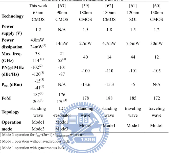
Table 3.2 Performance benchmark with SWO 35
Chapter 4
Table 4.1 Performance comparison with MMW DCO 51
Chapter 5
Table 5.1 Performance benchmark of MB-OFDM UWB frequency synthesizers 87
Chapter 6
Table 6.1 Designed parameters 99
Chapter 2
Fig. 2.1 The direct frequency synthesis of (a) direct digital synthesis and (b) direct analog
synthesis 5
Fig. 2.2 The indirect frequency synthesis 5
Fig. 2.3 The noise model of (a) indirect digital synthesis and (b) its simplified model 6 Fig. 2.4 The indirect frequency synthesis includes (a) ILFD-PLL (b) FM-PLL and (c)
RX-PLL 8
Fig. 2.5 (a) The conceptual ILFD circuit, (b) the diagram in frequency domain and (c)
locked spectrum 9
Fig. 2.6 The conceptual ILFM circuit 11
Fig. 2.7 The diagram of a frequency multiplier based on multiphase edge combining 12 Fig. 2.8 The diagram of an ADPLL 13
Chapter 3
Fig. 3.1 The diagram of feedback oscillatory system 17
Fig. 3.2 The diagram of a ring-type oscillator 17
Fig. 3.3 (a) A Colpitts oscillator and (b) A cross-coupled oscillator with differential output
18
Fig. 3.4 The phase noise of an oscillator 19
Fig. 3.5 Frequency tuning curve with multiband and single band 20
Fig. 3.6 Equivalent circuit for the LC oscillators 21
Fig. 3.7 A typical phase noise plot for a free running oscillator 21
Fig. 3.8 Conversion of noise to phase instabilities and phase noise sideband 22
Fig. 3.9 Circuit schematic of a (a) SSO and (b) DSO with N-MOS tail current 23
Fig. 3.10 Circuit schematic of a SSO with noise filtering technique 24
Fig. 3.11 (a) The LC tank QVCO and (b) its cell 25
Fig. 3.12 The conceptual diagram of QVCO 26
Fig. 3.13 Fig. 3.13 Measured frequency tuning curve of (a) the 8.4 GHz and (b) the 2.4
GHz VCO with multiband tuning 27
Fig. 3.15 (a) The proposed switched-mode standing wave oscillator architecture and (b)
detailed circuit schematic 29
Fig. 3.16 Standing wave oscillator for mode 3 operation 31
Fig. 3.17 Simulated Z11 at node l/2 with different excited mode 31 Fig. 3.18 SWO (a) chip micrograph and (b) physical layout 32
Fig. 3.19 Measured output spectrum at mode 1 (38 GHz) and mode 3 (114GHz) 33
Fig. 3.20 Measured phase noise before (grey) and after (dark) synchronous lock 34
Chapter 4
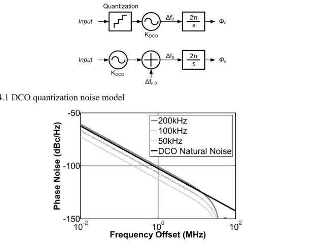
Fig. 4.1 DCO quantization noise model 38
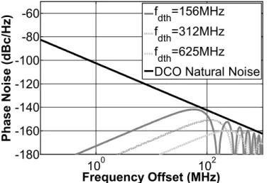
Fig. 4.2 Phase noise due to frequency quantization of different frequency resolution step
38
Fig. 4.3 Phase noise due to ΣΔ-shaped frequency quantization with different dithering
frequency 39
Fig. 4.4 Phase noise due to ΣΔ-shaped frequency quantization with different order of ΣΔ
modulator 39
Fig. 4.5 The front-end architecture for a 60 GHz dual-IF UWB system 41
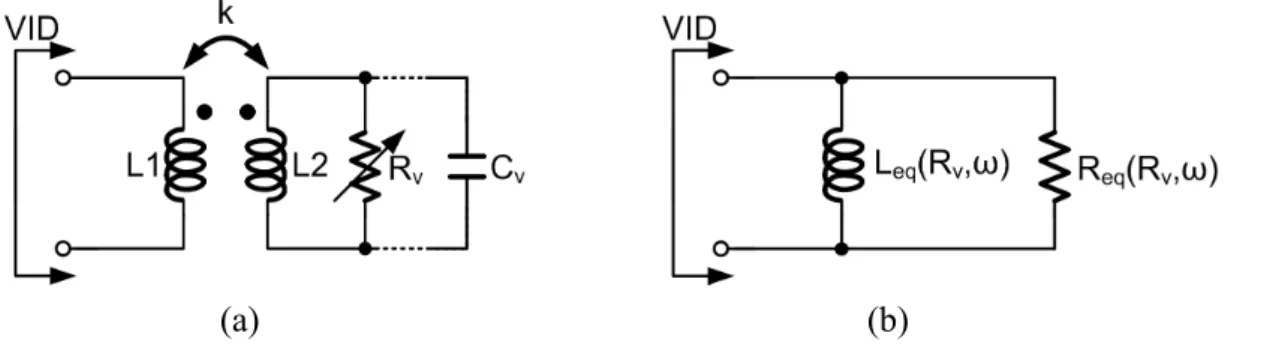
Fig. 4.6 (a) The proposed variable inductor (b) equivalent circuit model 42
Fig. 4.7 The 1:1 Transformer layout view 43
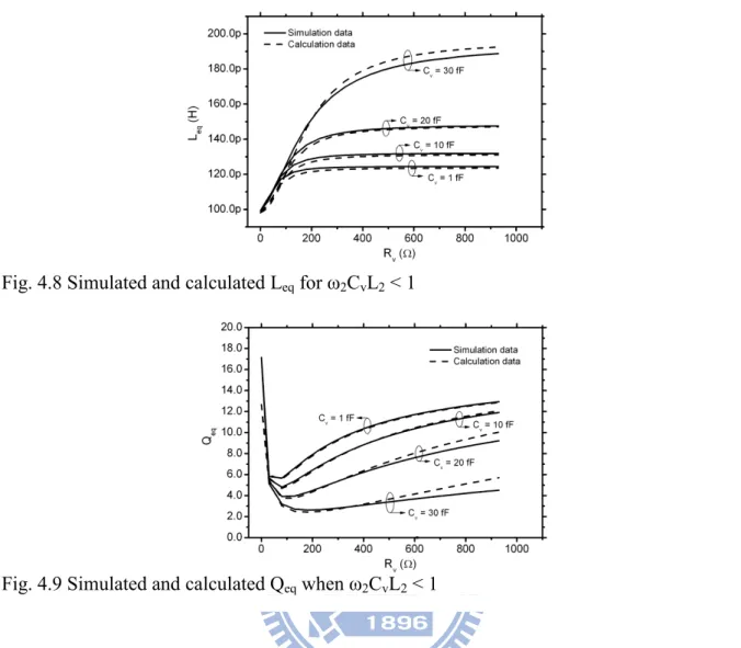
Fig. 4.8 Simulated and calculated Leq for ω2CvL2 < 1 44 Fig. 4.9 Simulated and calculated Qeq when ω2CvL2 < 1 44 Fig. 4.10 The calculated Leq and derived Rlin of the VID 45 Fig. 4.11 The reconfigurable transmission line 46
Fig. 4.12 The proposed 4-bits linear VID 47
Fig. 4.13 (a) The EM simulated and theoretic real part of Zeq and (b) equivalent inductance
and quality factor of linear VID 47
Fig. 4.14 The circuit schematic of DCO using 4-bits linear VID 48
Fig. 4.15 The chip microphotograph of DCO 50
Fig. 4.16. Measured frequency tuning range versus input code of the DCO 50
Fig. 4.17 Measured DCO phase noise at 10-MHz offset of the DCO 52
Fig. 4.18 Measured output spectrums at (a) 38 GHz (b) 41.6 GHz (c) 43.3 GHz 52
Fig. 4.21 The schematic of fine tune cell 56
Fig. 4.22 (a) The layout view and (b) the EM simulation results of the inductor 57
Fig. 4.23 Diagram of the 2nd MASH-II order ΣΔ modulator 57
Fig. 4.24 Chip microphotograph of the DCO applied to an ADPLL 58
Fig. 4.25 Measured DCO frequency versus control code of coarse tuning bank CDCO[24:18] 59
Fig. 4.26 Measured DCO frequency versus control code of fine tuning bank CDCO[17:8] 59 Fig. 4.27 Measure open loop phase noise from 9.98GHz carrier 60
Chapter 5
Fig. 5.1 The 14 bands frequency synthesizer architecture for MB-OFDM transceiver 64Fig. 5.2 Frequency planning for 14 bands carrier generation 65
Fig. 5.3 (a) Signal path for band 11 generation and (b) Signal spectrum at point A, B and C 66
Fig. 5.4 The simulated output spectrum of second stage SSB mixers with and without I/Q imbalance 69
Fig. 5.5 The trace diagram under (a) gain mismatch, (b) phase mismatch and (c) ratio of output vectors with phase and amplitude error during phase calibration 71
Fig. 5.6 The I/Q calibration architecture 72
Fig. 5.7 (a) The SSB mixer architecture and (b) the 1st stage SSB mixer 73
Fig. 5.8 The 2nd stage SSB mixer 74
Fig. 5.9 (a) Gain calibration buffer (b) I vector after gain calibration 75
Fig. 5.10 (a) Phase calibration buffer (b) Q vector after phase calibration 76
Fig. 5.11 (a) Gain and (b) phase simulation results of VCBUF 77
Fig. 5.12 (a) MUX1 and (b) MUX2 circuit schematic 78
Fig. 5.13 The charge pump circuit 79
Fig. 5.14 Chip microphotograph 80
Fig. 5.15 The measured PLL output spectrum 81
Fig. 5.16 The measured PLL phase noise 83
Fig. 5.18 The measured output spectrum at 3960 MHz (band 2) 84
Fig. 5.19 The measured output spectrum at (a) 7656 MHz (band 9) (b) 9468 MHz (band 13) and (c) 6600 MHz (band 7) 85
Fig. 5.20 Measured switching behavior from 8.1 GHz to 8.7 GHz 86
Chapter 6
Fig. 6.1 The wireless sensor network and bio-inspired electronics 89Fig. 6.2 (a) The proposed receiver architecture (b) frequency acquisition mode (c) phase tracking and data demodulation mode 91
Fig. 6.3 (a) Frequency discriminator (b) timing diagram of edge counter 92
Fig. 6.4 (a) QPSK signal constellation (b) demodulator (c) timing diagram 94
Fig. 6.5 (a) Receiver behavior model (b) equivalent model and (c) noise model 96
Fig. 6.6 The simulated settling behavior 99
Fig. 6.7 Low-noise amplifier based on (a) common-source and (b) common-gate topology 100
Fig. 6.8 The differential gm-boosted CGLNA 101
Fig. 6.9 The frequency down-converted mixer 102
Fig. 6.10 Post-amplifier architecture 103
Fig. 6.11 Gain cell of post-amplifier 104
Fig. 6.12 Full wave rectifier for RSSI 105 Fig. 6.13 The circuit schematic of charge pump and loop filter 105
Fig. 6.14 The architecture of (a) feedback divider, (b) timing diagram of divided-by-19 divider and (c) NAND gate embedded TSPC filp-flop 107 Fig. 6.15 Chip microphotograph 110
Fig. 6.16 Measured recover spectrum of the local oscillator 110
Fig. 6.17 Measured frequency locking time 111
Fig. 6.18 Measured phase noise performance 111
Introduction
In this chapter, the background and the organization of this dissertation are discussed. First, the background of frequency synthesis is introduced. Finally, the organization of this dissertation is well described.
1.1. Motivation
With the rapid development of communication system and CMOS technology, the circuit techniques of contemporary transceivers for wireless communication remain imperatively to be desired. Frequency synthesis is an essential technique in transceivers to perform a stable and high-purity local oscillator (LO) generation, or direct modulation transmission. These synthesizers need to meet the stringent requirements of low cost, low power and low voltage monolithic implementation while also meeting the phase noise and switching transient specifications. For varied communication systems, the frequency synthesizers have to face various challenges that need to be overcome.
In 2002, the Federal Communication Commission (FCC) regulations released the unlicensed spectrum from 3.1 to 10.6 GHz for ultra wideband (UWB) wireless communication. It opens an opportunity to develop a short range and high data rate communication for wireless personal area network (WPAN), or for wireless universal serial bus (USB). As proposed by MB-OFDM (multi-band orthogonal frequency division multiplexing) alliance, the spectrum for UWB communication system ranges is divided into 14 bands with each band of 528 MHz and categorized into 5 groups [1]. According to the recommendation, the frequency hopping time for band switching should be less than 9.5 ns. These challenges have drawn tremendous research efforts [2]-[18].
From the viewpoint of rapid evolution in CMOS technology, millimeter wave applications in sensing, advanced imaging, and bio-agent chemical detection become more feasible and have drawn tremendous research efforts in the past few years [55]-[64]. For pervasive adaptations, compact and cost-effective signal source is a key component to
2 Chapter 1. Introduction materialize these systems. Hence, CMOS synthesizers in nano-meter technology have strong potential to be applied in the sub-Tera Hz frequency range (0.1-1 THz).
Not only the opportunity of sub-THz application but also a highly integrated system on chip (SOC) is benefited by the advanced CMOS technology. However, it is difficult to integrate CMOS circuits including radio frequency, analog baseband and digital baseband on a single chip to achieve a solution of high volume, high power efficiency and effective cost. Therefore, a new paradigm of digital RF processor (DRP) [40]-[50] is reported. To take more advantages of nanometer CMOS technology, the RF circuits including frequency synthesizers are tried to be digitalized and be integrated at baseband. Hence, the all-digital phase locked loops (ADPLL) for SOC are reported [40]-[47], while the interface between continuous behavior of oscillators and discrete domain of digital circuits is an important issue. To conquer this issue, a high resolution digitally controlled oscillator is an essential circuit block.
On the other hand, the wireless sensor network (WSN) and bio-inspired electronics, which attract more stress on small form factor and low power, are another significant research [90]-[100], in contrast to consumer electronics pursuing maximum data rate. For bio-inspired electronics, the human signals, such as electrocardiogram, body temperature and blood pressure are monitored by wireless sensor node attached to the human body. Then the signals are transmitted to the medical server through portable wireless receiver. For the sensor node integrated circuits (ICs) design, small form factor, low power, and system cost are of special interests to promote pervasive and ubiquitous adaptations. Consequently, the transceiver ICs have to face these challenges for healthy electronics.
To sum up, the transceiver ICs need to have various research efforts to be adopted in specific communication systems. The stringent frequency hopping time of 9.5 ns is required for MB-UWB OFDM system. A signal source at sub-THz frequency band is required for sensing, advanced imaging or bio-agent chemical detection application. The frequency synthesizer at radio frequency needs to be digitalized for highly integrated SOC solution. Also, a small form factor and low power transceiver IC must to achieved to promote pervasive adaptations for disposable and healthy electronics. To conquer these various issues, this dissertation develops the frequency synthesis techniques and circuit skills for different challenges in recent communication systems.
1.2. Organization
Chapter 2 reviews different types of frequency synthesis technique and explores the characteristics between them. The direct, indirect and digital frequency synthesis is introduced and summarized in this chapter.
In chapter 3, the design considerations of a LC-type voltage controlled oscillator (VCO) are introduced. Then a 8.4 GHz and a 2.4 GHz VCO are implemented with experimental results, respectively. They will be respectively employed in chapter 5 and chapter 6 for proposed frequency synthesis. Furthermore, a switched-mode standing wave oscillator capable of generating fundamental and triple output frequency in sub-THz frequency range (0.1-1 THz) is proposed with experimental results. It can be further employed by a frequency multiplier based PLL.
In chapter 4, the design considerations of a LC-type digitally controlled oscillator (DCO) are introduced. Afterwards, a high resolution LC-type DCO at 10 GHz is designed and measured for an all digital PLL (ADPLL). Finally, a wide tuning range DCO at 40 GHz using proposed linear variable inductor are described with measurement for 60 GHz UWB system.
Chapter 5 describes a 14 bands CMOS frequency synthesizer with spurs reduction for MB-OFDM UWB system using direct frequency synthesis technique. The spurs issues encountered in direct frequency synthesis are investigated and analyzed. To alleviate the spurious tones, I/Q calibration algorithm applied in carrier generation are described. Moreover, the detailed circuit blocks are presented and experimental results of the synthesizer are discussed.
Chapter 6 demonstrates a 2.4 GHz single chip wireless receiver incorporating with frequency synthesizer without a need of resonator-based reference source. The receiver accomplishes LO carrier recovery and data demodulation directly from the RF received signal without a need of resonator-based reference source and extra baseband ADC. The established behavior model is included to discuss stability and noise issues. Then the major building blocks are presented. Finally, the experimental results are shown and discussed.
Chapter 7 summarizes the main results of this dissertation. The recommendations for future works are also addressed.
Chapter 2
Frequency Synthesis
Frequency synthesis is an essential technique employed in RF systems to achieve local oscillator (LO) generation or direct modulation transmission. In this chapter, we review the different types of frequency synthesis technique and explore the tradeoffs between them. The techniques of fractional-N synthesis typically are extended from integer-N. Thus we focus on the review of integer-N frequency synthesis. For a frequency synthesizer, the output signal purity, frequency settling time, frequency resolution and power consumption are important indexes. In section 2.2 the associated frequency synthesis technique is summarized for comparison.
2.1. Introduction
To constitute a complete data link for wireless communication system, one indispensable building block is required by both receive and transmit path. That is the building block which generates a stable local oscillator (LO) signal: the frequency synthesizer. Wherever frequencies are translated, frequency synthesis is crucial to provide a high purity, stable and programmable local oscillator signal. Depend on the requirement of communication systems, the frequency synthesizer may need to be fast switching to perform the addressing sufficiently fast, or it needs to be high purity since low oscillator noise is vital for the quality and reliability of the information transfer.
The techniques of frequency synthesis typically can be mainly categorized into two types. One is the direct frequency synthesis shown in Fig. 2.1(a)(b), and another is the indirect frequency synthesis shown in Fig. 2.2. Generally, the differentiation between direct and indirect techniques is determined by whether the synthesized loop is open or closed. The direct synthesis (open loop synthesis) can further be sorted as digital direct synthesis (DDS) and analog direct synthesis. Fig. 2.1(b) shows the diagram of DDS. DDS is a technique using digital data processing blocks as a means to generate a frequency and phase tunable output signal referenced to a fixed-frequency precision clock source. The major building blocks include a memory and a digital to analog converter (DAC). Due to the limited speed of the memory and high resolution DAC, high frequency operation is not feasible.
On the other hand, the analog direct synthesizer synthesizes the wanted output frequency from PLLs by multiplying, mixing and dividing, as shown in Fig. 2.1(b). By repeatedly mixing and dividing, any frequency spacing is possible to achieve. Besides, based on the direct frequency mixing scheme, the frequency hopping time is mainly depend on the switching speed of multiplexers and single sideband (SSB) mixers. Hence it results in fast settling time of only several nano-seconds. Ideally, the output spectrum is as clean as the reference sources from PLLs. However, when implementing the direct synthesizer, cross coupling and harmonic mixing between stages is a problem for the spectral purity and the large number of components causes the synthesizer to be power hungry. Thus the frequency mixing scheme of direct synthesis has to consider these practical issues. An ultra wideband
Memory (look-up table) Digital to analog converter (DAC) Clock fcontrol fout (a) PLL PLL MUX MUX fcontrol fout SSB mixers (b)
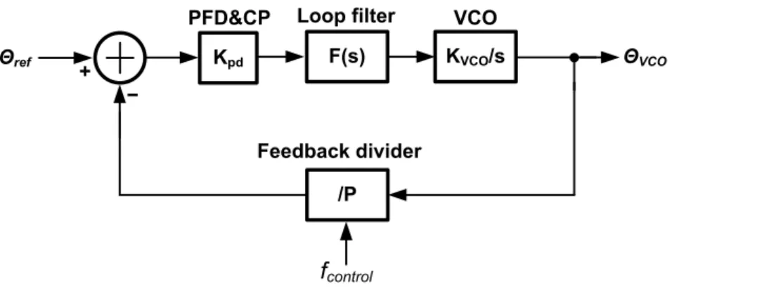
Fig. 2.1 The direct frequency synthesis of (a) direct digital synthesis and (b) direct analog synthesis ΘVCO PFD&CP F(s) Kpd KVCO/s VCO Loop filter /P Feedback divider Θref − + fcontrol Fig. 2.2 The indirect frequency synthesis
6 Chapter 2. Frequency Synthesis
(UWB) and fast settling frequency synthesizer utilizing open loop frequency synthesis will be demonstrated and analyzed in chapter 5.
The indirect frequency synthesizer generates its output by phase locking the divided output to a reference signal. Fig. 2.2 shows the block diagram of a closed loop frequency synthesis, where the gain of PFD and charge pump is Kpd, VCO gain is KVCO, and the transfer
function of loop filter is F(s). When a frequency hopping occurs, the loop need additional settling time to settle down since the loop configuration is readjusted by feedback divider. Generally, the settling time requires more than one hundred periods of reference cycle. It results in at least several micro seconds according to a typical reference frequency. The noise model of a PLL is shown in Fig. 2.3(a) and noise transfer function from each circuit blocks to output can be derived as
Θn,out PFD&CP F(s) Kpd KVCO/s VCO Loop filter 1/P Feedback divider Θn,fref − Θn,divider Θn,PFD&CP Θn,VCO (a) 0 f Sn,PFD 0 f Sn,VCO 0 f Sn,VCO
VCO referred noise
PFD referred noise
foptimal
(b)
( )
( )
( )
, , 1 n out n PFD referred A s P PG s A s θ θ − = + = (2.1)( )
( )
, , 1 1 1 n out n VCO referred G s A s θ θ − = + = − (2.2) where( )
1 PD VCO( )
A s = P K⋅ ⋅K ⋅F s sThe above can be observed that the noise come from reference signal, charge pump and feedback circuit contribute in band noise to output, while the VCO contributes out band noise. Fig. 2.3(b) shows the simplified noise model that the noise source is summarized as PFD referred noise (in band noise) and VCO referred noise (out band noise). It can be observed that in band noise is scaled by square of divide ratio and inverse of PFD gain. The optimal loop bandwidth is determined at the frequency that PFD referred noise meets the VCO referred noise. To suppress in band noise contributed from PFD and charge pump, a sub-sampling PLL were proposed [37]. This prior art improves the loop gain from charge pump to output, and mitigates the noise contributed from PFD and charge pump.
8 Chapter 2. Frequency Synthesis
For millimeter wave communication, a frequency synthesizer must generate high frequency LO for transceiver. However, the feedback frequency divider based on high speed D flip-flops is difficult to work at such high frequency. Therefore, some techniques for millimeter wave frequency synthesis were proposed [39], [55]-[59], [63]-[65]. Fig. 2.4 illustrates the indirect frequency synthesizers based on the techniques of injection locked frequency divider (ILFD), injection locked frequency multiplier (ILFM), multiphase edge combining, and the proposed receiver-based frequency synthesis.
H(s) Loop gain 1/P1 Θref − + ΘVCO PDivider 1/N1 ILFD VCO (a) H(s) Loop gain 1/P2 Θref − + PDivider × M VCO ΘVCO FM (b) G(s) Loop gain 1/P3 Θref − + ΘVCO PDivider Mixer VCO Nfref Post Amplifier RSSI (c)
Fig. 2.4 The indirect frequency synthesis includes (a) ILFD-PLL (b) FM-PLL and (c) RX-PLL
Fig. 2.5(a) shows the conceptual ILFD circuit [38]. By injecting a proper signal Iinj with
frequency ωinj into a resonant tank with a quality factor Q and center frequency ω0, the circuit
indeed oscillates at ωinj rather than at ω0 and injection locking occurs, as shown in Fig. 2.5(b).
The locking range of a injection locked phenomenon depend on the magnitude of injected signal Iinj and the quality factor of resonant tank Q and can be derived as [38]
M1 A1 -1 R1 L1 C1 Iinj I1 Iosc ωinj ω0 (a) ω ω Mag(tank) Phase(tank) ω0 ωinj (b) ω Power ω0 Injection locked Free running
Fig. 2.5 (a) The conceptual ILFD circuit, (b) the diagram in frequency domain and (c) locked spectrum
10 Chapter 2. Frequency Synthesis 0 0 2 2 1 2 1 inj L inj osc inj osc I Q I I I ω ω = ω ω− = ⋅ ⋅ − (2.3)
where Iosc denotes the magnitude of original oscillation tank, and ωL presents the locking
range. For Iinj <<Iosc, the above equation can be further approximated as
0 2 inj L osc I Q I ω ω ≈ ⋅ (2.4) Obviously, the frequency locking range of a injection locked circuit is proportional to the magnitude of injected signal and inversely proportional to the quality factor of oscillation tank. From the viewpoint of time domain behavior, a free running oscillator could be phase synchronized by an injected signal when injection locked occurs. The phase noise within the frequency range of ω0±ωL can be corrected likes a spectrum of phase locked, as shown in Fig.
2.5(c).
The ILFM and multiphase edge combining techniques can be summarized as frequency multiplier-based PLLs (FM-PLL). It is composed of a synthesizer with low frequency output cascaded with a frequency multiplier to generate the desired output frequency [39], [56]. In this structure, the low frequency synthesizer is operated at the sub-harmonic of the desired frequency and the target frequency is generated by the frequency multiplier such as ILFM [39] or multiphase edge combiner [56]. In contrast to fundamental mode PLLs, it has the smaller divide ratio and lower power dissipation from prescaler. However, the design of a low power and high conversion efficiency frequency multiplier is a key point.
The operation principle of an ILFM circuit is similar to an ILFD circuit which is based on the mechanism of injection locking. The nth harmonic term of the input signal is enhanced
by the nonlinear input stage and then injects to a tank which resonates at nth harmonic
frequency, as shown in Fig. 2.6. Typically, the input stage is designed to have an optimal gain at the wanted harmonic term.
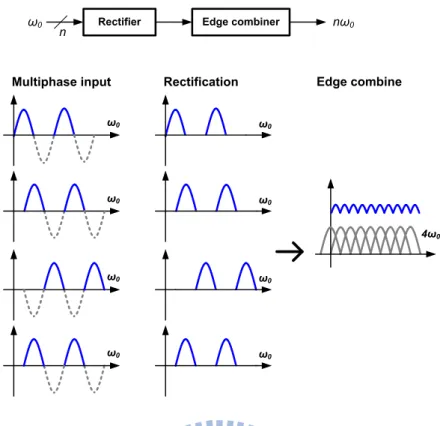
On the other hand, the multiphase edge combining technique employs linear superposition of multiple shifted phase (in 2π/n sequence, where n is an even integer) and rectified fundamental signals (at the angular frequency ω0) to produce a superimposed output
signal at the intended frequency of nω0. The diagram is illustrated in Fig. 2.7 by taking n=4
for example. The conversion efficiency from fundamental to nth harmonic can be derived as [56]
(
n 12)(
nn 1)
AIη= π⋅
− + (2.5)
where AI is the rectification gain. As the operating frequency increases, matching,
cross-coupling, and insertion loss of transmission lines between the oscillators and edge combiner become critical to the realization of a successful design. In addition, the edge combiner itself may become an obstacle to the achievement of the desired frequency range. These result in a low rectification gain (AI) and then low conversion efficiency (η). From the
perspective of power efficiency, an edge combiner seeks to eliminate lower order harmonics through vector cancellation. However, it turns out to consume a considerable amount of DC power wastefully since its output signal becomes quite small as the multiplication factor increases.
Furthermore, with the explosive growth of CMOS technology recently, the analog charge-pump based PLLs may encounter issues such as leakage from MOS capacitor, serious
M1 A1 -1 R1 L1 C1 Iinj I1 Iosc ωinj ω0~nωinj nonlinearity circuit
12 Chapter 2. Frequency Synthesis
current mismatch from charge pump circuits and limited voltage headroom under low power supply. These may lead to higher noise floor and spurious tone. Besides, the highly integrated level of an SOC allows more digital noise coupled to analog part. In other words, the analog circuit may not take too much advantage with the advance nano-meter technology. Consequently, the digital intensive approaches of PLLs have drawn tremendous research efforts recently [40]-[50]. The diagram of the all-digital PLL (ADPLL) is shown in Fig. 2.8. The ADPLL is mainly consisted of a digitally controlled oscillator, a time to digital domain interface and a digital loop filter. Although the ADPLL has advantages such as fast settling time, spurs free or direct modulation and so on [40]-[47], the resolution of the interface between continuous and discrete time domain is an issue and need extra efforts to overcome. In chapter 4, the proposed high resolution 10 GHz DCO and a wide tuning range 40 GHz DCO at is demonstrated respectively for 10 GHz ADPLL and 60 GHz UWB system.
To design a frequency synthesizer applying in THz image system, we propose a receiver-based PLL (RX-PLL) that employed a receiver-signal-strength-indicator (RSSI) to frequency tracking, as shown in Fig. 2.4(c). Because the VCO fundamental mode oscillates at THz such high frequency which almost closes to the maximum limitation in a CMOS technology, the output power is certainly small. Under this situation, the locking range of
Multiphase input Rectification Edge combine ω0 ω0 ω0 ω0 4ω0 ω0 ω0 ω0 ω0 Rectifier Edge combiner
ω0
n nω0
feedback divider must be small. Besides, the issues of the center frequency mismatch between ILFD and VCO due to PVT variation still exists. In contrast to an ILFD-PLL, the RX-PLL utilizes a frequency down-converted mixer to let the THz frequency down to intermediate-frequency and can be amplified by the proceeded post amplifier. Due to the low IF architecture, the magnitude of image tone caused by double sideband mixer can be filtered out below the noise floor.
Excepted to the crystal-based PLLs, a proposed crystal-less frequency synthesizer and receiver [99] will be introduced in chapter 6. Based on the concept of wireless remote frequency synchronization to the transmitter side, it eliminates extra reference generator at the receiver side, and also facilitates wireless clock distribution. Since the LO carrier at the receiver side is tracking the frequency at the transmitter side directly during data receiving, the issue of carrier frequency offset between the transmitter and receiver in conventional wireless transceivers is eliminated. Meanwhile, it accomplishes data demodulation along with carrier and timing recovery without resort to an extra base-band ADC.
2.2. Summary
This chapter introduces the synthesis techniques of direct frequency synthesis, indirect frequency synthesis, and proposed crystal-less frequency synthesis. The indirect frequency synthesis is based on the PLLs including ILFD-PLL, FM-PLL and RX-PLL. A frequency synthesizer has some important characteristics such as frequency locking range, frequency resolution, settling time, signal purity and power consumption. Table 2.1 summarizes the comparison of the indirect frequency synthesis techniques. Assume the following parameters are the same among them:
Reference frequency fref, target frequency fout, loop bandwidth of the PLL, frequency tuning
Digital loop filter DCO
PD F(z)
Θfref Θ
out
Analog to digital
14 Chapter 2. Frequency Synthesis
percentage of the VCO, power dissipation and noise of the circuit block are all the same Based on the assumption, the PLLs employ ILFD and ILFM have narrow frequency range limited by the nature of injection locking, while it generally consume less power than other techniques due to its high Q. At the point of frequency resolution, the FM-PLLs have worse resolution caused by the frequency multiplier. Also, the output power in FM-PLLs is smaller than the fundamental mode PLLs. Generally, the RX-PLL has wide locking range and faster settling time due to its inherent post amplifier can be employed to frequency tracking. The RX-PLL may intuitively be observed that it has larger in band noise than the other types due to it cascades two PLLs. However, the second PLL of the RX-PLL has larger loop gain from charge pump to output and the total PFD referred noise contributed to output can be derived as
(
)
, , 3 , n out RX PLL n PFD f − = N P f+ (2.6) Based on the assumption of same fout/fref, the RX-PLL has equal in band noise contributed from PFD referred noise of both two PLLs.In addition to indirect synthesis, the direct synthesis techniques can achieve ultra wide frequency locking range in contrast to indirect synthesis which is limited by VCO. Besides,
Table 2.1 Comparison of indirect frequency synthesis techniques
Reference ILFD-PLL
FM-PLL
RX-PLL ILFM Multiphase edge
combining
Frequency locking range narrow narrow wide wide
fout/fref P1N1 P2M P2M P3+N Frequency resolution
(normalized to fref) 1 M M 1
Settling time normal normal normal fast
Output power large small small large
PFD referred noise to output
(Normalized to ILFD-PLL) 1 1 1 1
the frequency settling time is faster than indirect synthesis than about 1000 times at the expenses of the circuit complexity and power consumption. These issues will be discussed in chapter 5. Moreover, a crystal-less frequency synthesizer and receiver [99] will be introduced in chapter 6.
Chapter 3
LC-Type Voltage Controlled Oscillator
This chapter introduces the design of LC-type oscillators for wireless communications. As discussed in chapter 1, the VCO plays an important role in a frequency synthesizer. For high frequency circuit designs, LC-type oscillators can achieve higher speed than ring-type oscillators, and have relatively good phase noise and ease of implementation. This chapter is focused on the design of LC-type oscillators and organized as follows. In section 3.2, the noise analysis in cross-coupled LC oscillators will be introduced [51]-[52]. By this noise analysis, the circuit technique for low noise design is presented [53]. Also, a performance comparison between only N-MOS (or P-MOS) and complementary is reported [54]. Two complementary VCO respectively operates at 8.4 GHz and 2.4 GHz both in 180 nm CMOS technology is implemented for an ultra wideband and fast settling frequency synthesizer in chapter 5, and for a crystal-less frequency synthesizer and receiver in chapter 6. In contrast to LC-type oscillators, a 38/114 GHz switched-mode standing wave oscillator (SWO) capable of synchronous locking [64] is presented in section 3.3 which can be utilized in a FMPLL. This section proposes a switched-mode standing wave oscillator capable of generating fundamental and triple output frequency in the sub-THz range by nature. Different excitation modes are enabled by digital control without resort to other high speed circuits or edge combiner. Additionally, incorporating mode enabling and sub-harmonic injection locking, the proposed SWO can be synchronized to an external reference to further improve phase noise performance. The close-in phase noise is improved by about 18 dB with the proposed scheme when the SWO is with synchronous lock. The experimental prototype was fabricated using a low leakage 65 nm 1P9M triple-well CMOS technology.
Oscillators are extensively used in frequency synthesis and clock generation. The design of oscillators on monolithic implementation can be categorized as ring-type and LC-type. Generally, ring-type oscillators consist of a number of gain stages in a loop. On the other hand, LC-type oscillators typically are also treated as a number of gain stages in a loop but with inductors in each gain stage. To sustain oscillation, the phase shift of a loop must be a positive feedback (or 360o), and the frequency that a positive feedback loop occurs determines the oscillation frequency. Besides, the other requirement is that the loop gain at the oscillation frequency must be larger than unity. Fig. 3.1 shows the diagram of feedback oscillatory system, and these two conditions are called “Barkhausen criteria”. The ring-type oscillators shown in Fig. 3.2 have output frequency as
1 2 osc d f n T = ⋅ (3.1) where n and Td is the number and the delay time of each gain stage. Frequency tuning is
achieved by varying the delay time which is dominated by the time of charge and discharge to output capacitor of each gain stage. The resulting tuning range is large. However, the circuit complexity limits the speed of ring oscillators. Also, the lack of noise filtering (as in LC-tank oscillators) and the transistors in the gain stages cause the intrinsically high phase noise. On the other hand, the oscillation frequency of a LC-type oscillator is determined by
H(s) In(s) β(s) Out(s) ( ) ( ) 0 H s β s ∠ = + + ( ) ( ) 1 H s β s ≥ ( ) ( ) 1 ( ) ( )( ) Out s H s In s = −H s β s
Fig. 3.1 The diagram of feedback oscillatory system
1 2 3 n
18 Chapter 3. LC-Type VCO
the resonance of an inductor and capacitor, as 1 osc tank tank f L C = (3.2)
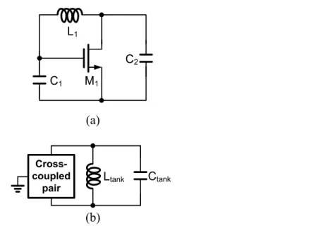
where Ltank and Ctank presents the inductor and capacitor values, respectively. Due to the
phase shift by inductors, a LC-type oscillator can satisfy the Barkhausen criteria with minimum gain stage. As shown in Fig. 3.3, a Colpitts oscillator demonstrates a topology of one stage and single-ended output, and a cross-coupled oscillator is a two stage and differential output topology which is commonly used in wireless communication. Due to its simple architecture and a band pass filter of LC-tank, LC oscillators perform relatively good phase noise and high resonant frequency. For wireless communications, the oscillators in a PLL operates at the highest frequency and usually determines the out band noise of the frequency synthesizer. For wireless communication, the out band noise picks up the interferers from adjacent channel and then degrades SNR of a receiver. Thus, this chapter focuses on the design of the LC-type oscillators. The considerations will be introduced in next section. In section 3.3, a switched-mode standing wave oscillator (SWO) capable of synchronous locking [64] which can be employed by a FMPLL is demonstrated.
M1 C1 C2 L1 (a) Cross-coupled
pair Ltank Ctank
(b)
3.2. Design Consideration
An oscillator generates a periodic output. The circuit must entail a self-sustaining mechanism that allows its own noise to grow and eventually become a periodic signal. According to Barkhausen’s criteria, a positive feedback loop and that the loop gain larger than unity are both vital requirements for oscillation. When design an oscillator for a wireless communication system, there are some important specifications need to take into considerations.
Phase noise: It is a parameter for signal purity in the frequency domain viewpoint. An
oscillator’s instabilities are usually characterized in terms of the single sideband noise spectral density shown in Fig. 3.4. It defines that the units of decibels below the carrier per Hertz (dBc/Hz) as
{ }
10log sideband(
0 , 1)
carrier P Hz L P ω ω ω + ∆ ∆ = (3.3)where Psideband(ω0+△ω, 1 Hz) denotes the single sideband power at a frequency offset
△ω from the carrier in a measurement bandwidth 1 Hz, and Pcarrier is the total power at
carrier frequency ω0. In the time domain viewpoint, the uncertainty of the transition
spacing is known as timing jitter. The clock jitter often dominates the maximum speed of digital circuits and high speed SERDES. A relation between phase noise and cycle to cycle jitter can be derived from the integral of phase noise profile [51]
1 Hz carrier P f
( )
V S ω ω ∆20 Chapter 3. LC-Type VCO
2 1 2 2 f f UI L f df J
(3.4)Frequency tuning range: The frequency tuning range of an oscillator dominates the
output frequency of a frequency synthesizer, and it must cover the entire frequency band for a communication system. The frequency tuning range usually designs larger than specification to cope with variation of process, voltage and temperature.
VCO gain: For a given noise amplitude on the control line of a voltage-controlled
oscillator, the noise in the output frequency is proportional to VCO gain (KVCO). Hence,
to minimize the effect of noise on the control line, KVCO must be minimized. There has a
constraint in direct conflict with the required tuning range. The multiband operation can be adopted to lower the sensitivity of the noise, as illustrated in Fig. 3.5.
Output power: Typically, the output of an oscillator drives next stages of frequency
dividers and mixers. Thus large amplitude swing at output is desirable to drive next stages. Besides, it has less sensitivity to noise when output power is large. The amplitude trades with power dissipation, supply voltage and even the tuning range.
Generally, a LC-type VCO has better phase noise and higher operating frequency than a ring-type VCO due to its higher quality factor. The equivalent circuit of a LC oscillator is
Vtune fosc ΔV Δfs s VCO f K V ΔfL ΔV L VCO f K V
Large KVCO Small KVCO
fosc
Vtune
shown in Fig. 3.6, which is composed of a RLC tank with loss and a positive feedback loop. To maintain oscillation, the loop gain must be larger than 1. The phase noise performance as well as start-up condition is both relative to effective series resistance in Fig. 3.6, which can be derived as [51]
(
)
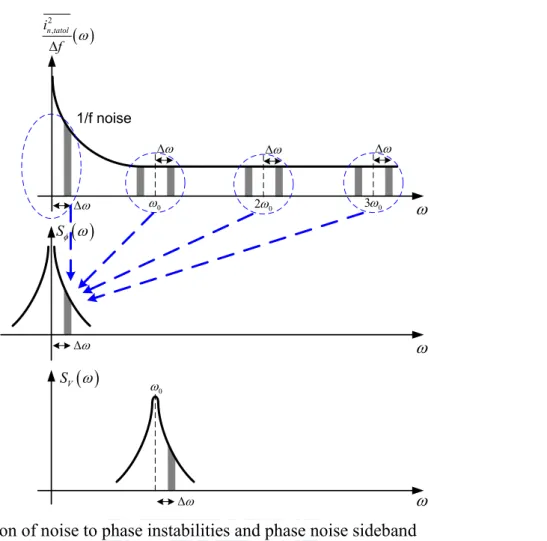
2 1 eff L C p osc R R R R ω C = + + (3.5)The above reveals that the more electric power stores in capacitor of tank, the more quality factor can be obtain. Also, effective series resistance can be reduced more to obtain better phase noise performance. A typical phase noise plot for a free running oscillator is illustrated in Fig. 3.7. The second order transfer function of LC-tank converts a flicker and thermal noise of circuits φinto 1/f3 and 1/f2 region, respectively. A flat region occurs at the
frequency far away from center frequency of LC-tank. To capture how the noise sources
Rp C L RC RL iin(ω) Gm Vout
Fig. 3.6 Equivalent circuit for the LC oscillators
( )
log ∆ω{ }
L ∆ω 1/f3 1/f2 / dBc Hz (-30 dB/dec) (-20 dB/dec)22 Chapter 3. LC-Type VCO
contaminate resonant tank, Fig 3.8 illustrates a diagram in spectrum. Fig 3.8 shows that noise components located near integer multiple of resonant frequency are integrated to form the low frequency sidebands for Sφ(ω). These sidebands in turn become close in phase noise as
SV(ω) through phase modulation. The close-in (1/f 3 region) phase noise is mainly caused by
the flicker noise of tail current through the mechanism of up-converted single balance mixer performed by cross-coupled pair [53], or a time-variant phase noise model with impulse sensitivity function [51]. Then the 1/f 3 noise due to tail current will be further filter out by
LC-tank band pass filter, which is depend on its quality factor. On the other hand, the noise in 1/f 2 region is deteriorated by cross-coupled pair and effective series resistance of tank. The
[51] derived phase noise in 1/f 2 region and 1/f 3 region is described as
{ }
22 2 2 max 10log 2 rms in f L q ω ω Γ ∆ ∆ = × ⋅ ∆ for ω ω> 1/ f (3.6) ω ∆ ω ∆ 0 3ω ω ∆ 0 2ω 1/f noise ω ∆ 0 ω ω ∆ ( ) 2 , n tatol i f ω ∆ ω ω ∆ 0 ω ω ω ( ) Sφ ω ( ) V S ω{ }
02 2 1/ 2 2 max 10log 2 f n c i f L q ω ω ω ω ∆ ∆ = × × ⋅ ∆ ∆ for ω ω< 1/ f (3.7)where Γrms and C0 respectively denote the root-mean-square and DC value of ISF, qmax is the
maximum charge stored in tank and ω1/f is the corner frequency of device.
The cross-coupled LC oscillators can be categorized as double-switch-pair oscillator (DSO) and single-switch-pair oscillator (SSO) two types. Fig. 3.9 illustrates the circuit schematics of SSO and DSO both with N-MOS tail current source, and their noise source are contributed from cross-coupled pairs, tail current, and LC tank itself. The phase noise in 1/f2 region for DSO and SSO can be respectively derived [54]
( )
( )
2 2 2 tan 10 log 1 2 n p B DSO DSO k p k T L A C R γ γ ω ω + ∆ = + ∆ for DSO (3.8)( )
( )
2(
)
2 2 tan 10 log B 1 SSO n SSO k p k T L A C R ω γ ω ∆ = + ∆ for SSO (3.9)The γp and γn presents the channel noise of P-MOS and N-MOS, respectively. Assume γp and
γn are equal, and everything else is also the same, except the oscillation amplitudes Adso and
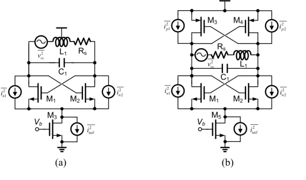
M1 M2 Vb L1 C1 2 2 n i 2 1 n i 2 tail i Rs M3 2 rs v
M1 M2 Vb L1 M3 M4 C1 Rs 2 1 n i 2 2 n i 2 1 p i 2 2 p i 2 tail i 2 rs v M5
(a) (b)
24 Chapter 3. LC-Type VCO
Asso. We have seen that, for the same bias current, the DSO has double oscillation amplitude,
compared to the SSO and results in a phase noise which is 6 dB lower in the DSO. It figured out that DSO does not have to pay any noise penalty associated to the second switch pair. In fact, what happens is that each switch in the DSO generates only half as much noise as each switch in the SSO, so that the total noise is the same in both oscillators.
Although DSO has better phase noise performance when operating at the same bias current and power supply, the SSO can operate at half power supply and twice bias current to achieve the same FoM of DSO, as summarized in Table 3.1 which the values are normalized to DSO. Therefore, SSO is suitable for low voltage supply than DSO by its nature. On the other hand, if a chip with power management cannot offer an extra half power supply to SSO, DSO is more properly to be adopted in this situation.
To suppress more phase noise, a noise filtering technique can be adopted [53]. As discussed before, noise components located near integer multiple of resonant frequency are
Table 3.1 Comparison with DSO and SSO
DSO SSO
VDD 1 1 0.5
Itail 1 1 2
Phase noise 1 0.25 1
Figure of merit 1 0.25 1
integrated to vicinity of resonant frequency results in close in phase noise. Hence, we can design a filter to filter out the significant noise in 2ω0 to achieve a low noise oscillator. Fig
3.10 illustrates a SSO with noise filtering technique. A top bias with P-MOS has adopted to obtain lower flicker noise floor, a bypass capacitor at node A also utilizes to bypass the noise at 2ω0. Besides, an auxiliary LC-tank is added at the source of cross-coupled pair and
resonates at 2ω0 to prevent gds of the switch pair in triode region to degrade the quality factor
of LC-tank.
A quadrature VCO (QVCO) and a differential VCO respectively operates at 8.4 GHz and 2.4 GHz is implemented using 180 nm CMOS technology. Under a single 1.8 V power
Iout Ioutb Qout Qoutb I Ib O Ob Vb Vtune I Ib O Ob Vb Vtune Cell_1 Cell_2 Vb Vtune VBS (a) M1 M2 M3 M4 Cc1 Cv2 Cc2 R1 R2 M5 M6 L1 Cv1 Vtune Vb Ib O I I1 I2 2 vBS SC2 Ob 2 vBS SC1 (b) Fig. 3.11 (a) The LC tank QVCO and (b) its cell
26 Chapter 3. LC-Type VCO
supply, both of them are base on a complementary architecture. Fig. 3.11 illustrates the LC tank QVCO and its core cell. Both Cv1 and Cv2 are accumulation mode MOS varactors for
fine frequency tuning. In addition, the switched capacitor SC1 and SC2 are added in parallel
for coarse tuning to cope with PVT variations. The quadrature output employs anti-phase coupling technique to form a two stage ring oscillator between two differential VCOs. By injecting out phase current to tank through M5 and M6, the oscillation frequency must deviate from ωcenter by a greater amount so that tank provides the required phase shift, as
shown in Fig. 3.12. As the frequency is increasingly farther from the resonant frequency, the Q falls and the phase noise raises as well. Thus it is desirable to sustain anti-phase coupling while minimize the coupling factor defined as
1 2 I coupling factor I = (3.10)
A coupling factor of approximately 25% typically provides a reasonable compromise between Q degradation and oscillation reliability for synchronization. Under this condition, the oscillation frequency can be derived as
1 1 1 4 osc Q LC ω = × − (3.11) ω ω Mag(tank) Phase(tank) ωcenter ωosc Φshift
Fig. 3.13(a) shows the measured oscillation frequency versus tuning voltage under 2 bits coarse tuning. The oscillation frequency of QVCO can cover the wanted frequency of 8448 MHz at code 01 while drawing about 5 mA from a 1.8 V power supply. The QVCO will be employed in chapter 5 to design an ultra wideband and fast settling frequency synthesizer. On the other hand, Fig. 3.14 shows another complementary VCO operating at 2.4 GHz. The 2.4 GHz VCO have 3 bits coarse tuning due to the requirement of low KVCO. The design policy is
the same with QVCO and the measured oscillation frequency versus tuning voltage under 2 bits coarse tuning is shown in Fig. 3.13(b). The VCO consumes 2 mA under a 1.8 V power
(a)
(b)
Fig. 3.13 Measured frequency tuning curve of (a) the 8.4 GHz and (b) the 2.4 GHz VCO with multiband tuning
28 Chapter 3. LC-Type VCO
supply with KVCO around 100 MHz/V. This 2.4 GHz VCO will be utilized in Crystal-less
frequency synthesizer and receiver introduced in chapter 6.
3.3. Switched-Mode Standing Wave Oscillator
Millimeter wave applications in sensing, advanced imaging, and bio-agent chemical detection have drawn tremendous research efforts in the past few years. For pervasive adaptations, compact and cost-effective signal source is a key component to materialize these systems. Recently, CMOS oscillators in nano-meter technology have demonstrated strong potential to be applied in the sub-Tera Hz frequency range (0.1-1 THz) [55]-[57]. These designs are basically based on LC-tank architecture and try to multiply its output frequency through a multi-phase edge combing [56] or push-push techniques [57]. As the operating frequency advances to hundreds of GHz range, matching, cross-coupling, and insertion loss of transmission lines between oscillators and edge combiner become more and more critical for a successful design. Besides, the edge combiner itself may become the bottleneck of the achievable frequency range. From the view point of power efficiency, edge combiner tries to eliminate lower order harmonics by vector cancellation. It turns out to burn a lot of DC power in vain since its output signal becomes quite small for a higher multiplication factor.
M1 M2 M3 M4 C1 C2 C3 C4 R1 R2 SC1 2 voutp vBS SC2 2 voutn vBS I1 vtune vbias
In contrast to LC-tank oscillators, wave-based oscillators are capable of pushing their output frequency close to devices’ cut-off frequency (fT) by distributing parasitic capacitance
along the transmission line [58]-[62]. The output frequency can be varied by switching capacitor and varactor tuning [60]. Under the ultimate frequency limitation, the oscillation speed is primarily determined by the characteristics of the transmission line. Conventional standing wave or traveling wave oscillator or distributed oscillator is operated at its fundamental mode [58]-[62], and is difficult to generate double or triple output frequency in a single oscillator in contrast to its multi-band LC oscillator based counterparts [9]. In order to facilitate multi-band operation, this section proposes a switched-mode standing wave
(a)
(b)
Fig. 3.15 (a) The proposed switched-mode standing wave oscillator architecture and (b) detailed circuit schematic