國 立 交 通 大 學
電子工程學系 電子研究所碩士班
碩 士 論 文
低溫多晶矽技術對多晶矽奈米線薄膜電晶體
通道結晶特性影響之研究
A Study of Characteristics of Poly-Si Nanowire Thin-Film
Transistors Fabricated by LTPS Technique
研 究 生:林漢仲
指導教授:林鴻志 博士
黃調元 博士
低溫多晶矽技術對多晶矽奈米線薄膜電晶體
通道結晶特性影響之研究
A Study of Characteristics of Poly-Si Nanowire Thin-Film
Transistors Fabricated by LTPS Technique
研 究 生:林漢仲 Student:Han-Chung Lin
指導教授:林鴻志 博士 Advisor:Dr. Horng-Chih Lin
黃調元 博士
Dr. Tiao-Yuan Huang
國 立 交 通 大 學
電子工程學系 電子研究所碩士班
碩 士 論 文
A Thesis
Submitted to Department of Electronics Engineering & Institute of Electronics College of Electrical and Computer Engineering
National Chiao Tung University in Partial Fulfillment of the Requirements
for the Degree of Master in
Electronics Engineering June 2008
Hsinchu, Taiwan, Republic of China
低溫多晶矽技術對多晶矽奈米線薄膜電晶體
通道結晶特性影響之研究
研 究 生:林漢仲 指導教授:林鴻志 博士
黃調元 博士
國立交通大學
電子工程學系 電子研究所碩士班
摘 要
本論文研究應用低溫多晶矽(LTPS)技術,製造具有多晶矽奈米線通道
之薄膜電晶體。快速熱退火(RTA)是一種具有材料選擇性加熱的技術,應
用於金屬誘發側向結晶法(MILC)時,除了可以大幅降低元件製程時間和
熱積存問題,更能增加複晶矽橫向結晶的速度;然而,固相結晶(SPC)機
制的發生卻會使 MILC 反應受到阻礙,藉由調整 RTA 製程溫度與持溫時
間,討論元件特性造成的影響;並從材料、電性分析和活化能等參數萃取,
探討成核開口配置及不同結晶方法製備奈米線通道薄膜電晶體的差異。另
外,當電晶體佈局為複數通道時,不同多晶矽結晶技術將會對元件通道多
晶矽品質產生變異性,進而造成元件操作特性的擾動,本研究結果顯示
MILC 製程採用 RTA 技術,在生產製造奈米線通道之薄膜電晶體,元件
特性的均勻性優於一般採用爐管製備法。
A Study of Characteristics of Poly-Si Nanowire Thin-Film
Transistors Fabricated by LTPS Technique
Student:Han-Chung Lin Advisors:Dr. Horng-Chih Lin
Dr. Tiao-Yuan Huang
Department of Electronics Engineering & Institute of Electronics
National Chiao Tung University
ABSTRACT
In this thesis, low-temperature poly silicon (LTPS) technique is employed to fabricate TFTs with poly-Si nanowire (NW) channels. Rapid thermal annealing (RTA) not only possesses a good selective heating function with specific materials, but the process time and the issue of thermal budget can be diminished, even re-crystallization rate of a-Si is increased during metal-induced lateral crystallization (MILC) process. However, the mechanism of solid phase crystallization (SPC) takes place earlier in the film as the crystallization temperature increases; the laterally-grown cryststalline grain of MILC is blocked. By adjusting RTA temperature and annealing time, the impacts on the performance of the fabricated NW-TFTs are discussed. The effects of seeding window arrangement and different crystallization strategy are investigated as well via material analysis, electrical characteristics, and extraction of activation energies. Moreover, there exists crystalline variation among the poly-Si NWs. Therefore, the fluctuation of NW-TFT performance is observed. In this regard, our results indicate that MILC process with pulsed RTA (PRTA) technique achieves better uniformity in device characteristics
誌 謝
碩士班兩年的求學過程中,由衷感謝林鴻志教授與黃調元教授的指
導,培養了我做研究應有的正確態度與追求知識的執著。每天進進出出
NDL做實驗的日子令我難忘,感謝蘇俊榮、盧景森、張凱翔、徐行徽、蔡
子儀、林哲民等學長的提攜,帶領我完成實驗,也鉅細靡遺的與我分享你
們豐富的經驗;謝謝好同學們,陳威臣、劉大偉、洪政雄、洪文強、李冠
樟、江忠祐和陳玲,因為有你們讓我在求學路上不寂寞,在彼此互助、討
論和學習之下,建立了深厚的友誼。ADTL實驗室是一個大家庭,蓬勃的
朝氣讓大夥有向心力,每一位成員都是實驗室的一股活力,能和大家在一
起做研究是緣分,也是三生有幸。最後,謹以本文獻給最敬愛的父親林裕
章先生、母親劉月卿女士,感謝多年來給予我堅強的後盾,讓我得以全心
全意投入研究領域,完成夢想,也特別感謝姊姊湘怡長期的陪伴父母與對
我的支持,讓我求學無後顧之憂。期許自己秉持學海無涯、立志終身學習,
更希望所學能對產業有所貢獻。
漢仲 謹誌於 新竹交通大學 2008 年 6 月Contents
Abstract (in Chinese)……….………...i
Abstract (in English)………...……….ii
Acknowledgement (in Chinese)………..…………iii
Contents……….………...………iv
Table Captions………...………...………vi
Figure Captions………...………….…...vii
Chapter 1 Introduction………...……..1
1.1 Overview of LTPS TFT……….………….1
1.1.1 Solid Phase Crystallization (SPC).………...……….2
1.1.2 Excimer Laser Crystallization (ELC)………..…………..3
1.1.3 Metal-Induced Lateral Crystallization (MILC)………...…..…………4
1.2 Overview of Nanowires………..5
1.3 Pulsed Rapid Thermal Annealing MILC of a-Si Film………7
1.4 Thesis Organization………...………….8
Chapter 2 Device Fabrication and Measurement………..………..10
2.1 Device Structure and Process Flow……….……….……10
2.2 Measurement Setup and Electrical Characterization………...……….12
Chapter 3 NW-TFTs Fabricated by Pulsed RTA MILC………..………...14
3.1 Material Analysis of PRTA Grain Growth………14
3.4 Effects of Pulsed RTA Annealing Conditions……….….………….19
3.4.1 Effects of Pulsed RTA Annealing Temperature………...……….19
3.4.2 Effects of Pulsed RTA Annealing Time……….………...…..…….21
3.5 Leakage Mechanisms………..………..22
Chapter 4 NW-TFTs Fabricated Using Different Crystallization Strategy…….….….25
4.1 The Effect of Stress on PRTA NW-TFTs………..……25
4.2 The Effect of Crystallization Approaches……..………...26
4.2.1 Comparison between Furnace and PRTA Annealing MILC…………..……..26
4.2.2 MILC NW-TFTs with Multiple Channels………..……..28
4.3 The Fluctuation of NW-TFTs………29
Chapter 5 Conclusion and Future Work………..32
5.1 Conclusions………..………32 5.2 Future Work………...………..…….33 References………..…..35 Table………...………..42 Figure………...……….………...…46 Vita………...…..………..81
Table Captions
Chapter 1
Table 1-1 The comparisons among SPC, ELA, and MILC. ………..………..42
Chapter 3
Table 3-1 Key electrical parameters of NW-TFTs with SSW configuration by PRTA MILC. ………..43
Chapter 4
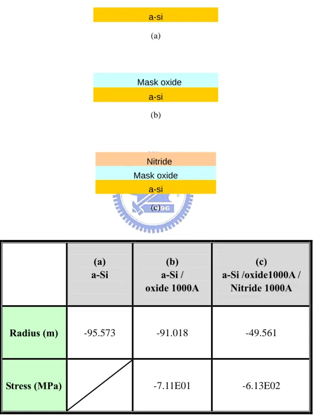
Table 4-1 Stress Measurements of LTO and Nitride films deposited on a-Si layer. …...44
Table 4-2 Major parameters for NW-TFTs by three different crystallization approaches. ………45
Figure Captions
Chapter 1
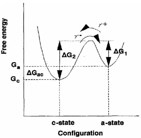
Fig. 1-1 Schematic illustration of the free energy of a- and c-states. ………...….46
Fig. 1-2 (a) Equilibrium molar free-energy diagram for NiSi2 in contact with a-Si and c-Si. (b) Schematic representation of the proposed NiSi2 and growth of c-Si. ……....47
Chapter 2
Fig. 2-1 Key device-fabrication flow. ………..……….….48
Fig. 2-2 (a) Top view of NW-TFTs and (b) the definition of poly-Si nanowire channel...50
Fig. 2-3 TEM images of NW-TFT without Nitride-capping layer. ………...…51
Fig. 2-4 TEM images of NW-TFT with Nitride-capping layer. ………....52
Chapter 3
Fig. 3-1 (a) Heating temperature in one cycle annealing during PRTA. (b) On/Off status of the heating lamp and a illustration of measured temperature in RTA processor. ………...…53
Fig. 3-2 Growth of the MILC region using PRTA with different annealing peak temperature (On/Off time of PRTA per one cycle is 10/30 sec). …………..…54
Fig. 3-3 Illustration of competing crystallization mechanisms between MILC and background SPC. ………...55
Fig. 3-4 Activation energies of MILC for PRTA and furnace annealing. ………...56
Fig. 3-5 The schematic device structures of two kinds of MILC seeding window arrangement, including (a)ASW and (b) SSW configuration. ………...57
Fig. 3-6 Optical microscopic images of the growth of MILC region with increasing pulsed cycles. ………....58
channel length. ……….…..59
Fig. 3-8 (a) Transfer and (b) output characteristics of NW-TFT by PRTA MILC. ….….60
Fig. 3-9 Transfer characteristics of NW-TFTs with Nitride capping layer. ……….61
Fig. 3-10 Transfer characteristics of NW-TFTs without nitride capping layer. ……….…62
Fig. 3-11 Transfer characteristics of NW-TFTs fabricated by PRTA anneal at 675°C. ….63
Fig. 3-12 A schematic of possible flow paths for off-state leakage currents. …………....64
Fig. 3-13 Leakage mechanisms in the gate-to-drain overlap region. (a) Thermal emission. (b) Thermionic field emission. (c) Band-to-band tunneling. ………….………65
Fig. 3-14 Transfer characteristics of NW-TFT with (a) ASW and (b) SSW configuration measured in forward/reverse operation mode. ………..66
Chapter 4
Fig. 4-1 Transfer characteristics of NW-TFTs with or without Nitride capping layer. ...67
Fig. 4-2 Cumulative probability of (a) subthreshold swing and (b) threshold voltage of NW-TFTs with or without nitride capping layer. ……….…...68
Fig. 4-3 (a) Transfer and (b)output characteristics of NW-TFTs with ASW configuration fabricated by furnace MILC. (c)Transfer and (d)output characteristics of NW-TFTs with SSW configuration fabricated by furnace MILC. ……….……69
Fig. 4-4 (a)Transfer and (b)output characteristics of NW-TFTs fabricated by furnace SPC. ……….…...…71
Fig. 4-5 Transfer characteristics of NW-TFTs fabricated by MILC (both PRTA and furnace anneal) and SPC (furnace anneal). ……….…...72
Fig. 4-6 Plot of ln(ID/VG) versus (1/VG) for three different crystallization approaches...73
Fig. 4-7 Schematic illustrations of ASW and SSW NW-TFT with multiple channels….74
Fig. 4-8 Transfer characteristics of NW-TFTs with multiple channels fabricated by furnace MILC. ………....75
Fig. 4-9 Transfer characteristics of NW-TFTs with multiple channels fabricated by PRTA MILC. ………76
Fig. 4-10 On-current as a function of the multiple channels for NW-TFT devices crystallized by MILC : (a) furnace anneal (ASW configuration), (b) furnace anneal (SSW configuration), (c) PRTA (SSW configuration), and (d) crystallized by furnace SPC. ……….78
Fig. 4-11 Comparisons of on-current for PRTA and furnace MILC NW-TFTs with multiple channels. ………..79
Fig. 4-12 Cumulative probability of (a) subthreshold swing and (b) threshold voltage of NW-TFTs fabricated by three different approaches. (i.e., MILC by either PRTA or furnace anneal, and SPC by furnace anneal) ……….……80
Chapter 1
Introduction
1.1 Overview of LTPS TFT
Low-Temperature Poly Silicon (LTPS) Technology has drawn much attention from
many research organizations around the world, and has been widely recognized as one of
the most important next-generation large-area electronic techniques. Owing to electrical
performance and cost-down issue, various functional devices such as displays, sensors,
memories, and even other 3-dimensional complicated integrated circuits regard LTPS as a
potential solution for the future. Poly silicon (poly-Si) thin film transistors (TFTs) are in the
vanguard of technological advancement. With their higher carrier mobility and drive
current, poly-Si TFTs can be employed for reducing pixel charging time of the periphery
circuits of the display [1], [2]. Poly-Si TFTs are also expected to enable all the computing
electronics to be built on the display itself, while larger aperture ratio and higher panel
resolution can be achieved. Moreover, the manufacturing of poly-Si TFT can be
implemented with CMOS process on the inexpensive glass substrates, leading to cheaper
expenditure. Currently there are several approaches for the preparation of LTPS films,
including solid-phase crystallization (SPC) [3], metal-induced lateral crystallization (MILC)
mentioned methods for LTPS is summarized in Table 1-1. Details would be explained as
follows.
1.1.1 Solid Phase Crystallization (SPC)
SPC is a common method to transfer poly-Si from a-Si. The process was typically
carried out in a furnace with N2 carrier gas and annealing temperature of approximately
600°C for several hours. The phase transition of amorphous (a-) state to crystalline (c-)
state consists of incubation and crystallization steps, where the kinetics can be described
respectively by classical nucleation and conventional thermodynamic theory [6], [7]. Also
noted that an important parameter of phases transition, the Gibbs-free-energy difference
(∆G), is correlated with the nucleation rate and grain growth velocity as shown in Fig. 1-1
[8].
Similar to most solid-state transformation, a crystalline film can nucleate
homogeneously within the amorphous film or heterogeneously on interfaces or defects
which serve as the nucleation centers, and then gradually grow until two adjacent grains
contact with each other, forming a region called grain boundary (GB). There exist grain
boundary dangling bonds and intra-grain strain bonds in poly-Si of SPC; as a result, the
characteristics were influenced. Hence, NH3 [9], H2 [10], and O2 [11] plasma treatments for
eliminating trap defects are widely used for poly-Si TFTs. The detailed physical
mechanism and kinetics of plasma passivation have been well reported [12].
1.1.2 Excimer Laser Crystallization (ELC)
Concerning mass production of TFT applications such as active-matrix liquid-crystal
displays (AMLCDs), ELC presently has become the most promising LTPS technique [13].
The laser light sources are generated by standard gas mixtures, XeCl (308nm), KrF
(248nm), and ArF (193nm). As a short-pulsed, rectangular UV beam is scanned across the
substrate, the amorphous silicon film is melting first and solidified to the crystalline state
when it cools. It is a high-throughput process because of high laser beam energy.
Excimer-laser crystallized poly-Si, however, has a serious problem that the grain size is less
than 100 nm with non-optimized process conditions [5], [14]. Besides, if laser energy
density is not be well-controlled and reproduced over time, non-uniform and randomly
distributed poly-Si grains will result in large variation of TFT performance, particularly for
small-dimensional TFTs fabrication [15]. Fortunately, many approached have shown that
large grains with uniform grain size distribution can be achieved, including sequential
continuous-wave laser lateral crystallization [19], selectively enlarging laser crystallization
[20], etc. However, some of them are not readily compatible to existing ELA systems or an
adequate solution for circuit layout due to the large amount of existing anisotropic grain
boundaries.
1.1.3 Metal-Induced Lateral Crystallization (MILC)
Metal-induced crystallization (MIC) of amorphous silicon has intensely been
investigated over the past few decades. It was known that certain metals contact with a-Si
would act as a catalyst for inducing the crystallization at a lower temperature. Film
crystallinity superior to SPC can be achieved. Owing to different reactions which are taking
place at metal/silicon interface, the crystallization mechanism can be classified into two
groups. One uses metals, for example Al [21], Au [22] and Sb [23] to form eutectics with Si.
The other forms silicide with Si by using Ti [24], Pd [25] and Ni [26]. It is believed that
metal dissolved in a-Si may weaken Si bonds and enhance the nucleation of crystalline
silicon [27]. However, problems related with metal contamination of the crystallized Si
films must be solved. Fortunately, it has been reported that a-Si thin film can be
crystallized laterally with less metal tainting. This process is called metal-induced lateral
high-performance TFTs.
Compared with the microstructure of conventional poly-Si with fine grains, MILC
poly-Si consists of relatively elongated grains and less grain boundaries in the crystalline
film [28]. In general, Ni was chosen as the catalytic material. During MILC process at a
temperature around 500°C, NiSi2 crystallites were formed and laterally migrated through
a-Si. The driving force for the transformation of a-Si to c-Si is the free energy difference.
As shown in Fig. 1-2, the chemical potential of Ni atoms is lower at the NiSi2/a-Si interface,
whereas the chemical potential of Si atoms is lower at NiSi2/c-Si interface [29]. In other
words, the migration of Ni atoms consumes a-Si is at NiSi2/a-Si interface and needlelike Si
crystallines are generated at the other side of NiSi2. Furthermore, the lattice constant of
NiSi2 is 5.406 Å, which is 0.4 % less than that of Si (5.430 Å), and is truly a good nucleus
of Si for induced crystallization, excluding the phenomenon of misfit dislocation.
1.2 Overview of Nanowires
Nanoelectronics refers broadly to a field of applied science and technology that can
precisely control matter on the atomic or molecular scale, generally with dimensions
smaller than 100 nm. The nanowires (NWs) are especially intensely interesting due to their
many potential emerging device applications, including nano CMOS [30], memories [31],
NW-TFTs [32], biochemical sensors [33], [34], and light-emitting diodes [35]. There are
two main approaches for Si-NW preparation, as described in the following.
(a) Bottom-up
A bottom-up approach signifies that the materials or devices are built from molecular
components which are assembled chemically. The synthesis of Si-NWs with small diameter
can be achieved by catalyst-assisted growth. The vapor-liquid-solid (VLS) growth
mechanism is one of the most developed methods for this approach [36]. Formed NWs are
later harvested and dispersed into a solution, assembled and aligned on the desired
substrate and are demonstrated that they can be carried out by electrical-field-directed
assembly [37], microfluidic channel [38], and Langmuire-Blodgett (LB) technique [39] etc.
Although the bottom-up approach offers great potential in nanoelectronic [40], [41], the
reproducibility and controllability of NWs hedge about its use in practical manufacturing
nowadays.
(b) Top-down
A top-down approach employs advanced lithographic tools like deep UV stepper, e-beam
writer or nanoimprint [13]. Compatible with modern semiconductor process, patterns
as it requires expensive equipments and cutting-edge technologies. The dimension of NW
is also confined by the resolution limit of lithography and the capability of etching. Thus,
several special techniques such as thermal flow, chemical shrink, and spacer patterning [14]
have been proposed that uncomplicated methods can directly generate nano-scale patterns
via conventional lithography tools (e.g., I-line and G-line steppers).
1.3 Pulsed Rapid Thermal Annealing MILC of a-Si Film
Very high performance TFT with local grain quality similar to that of single crystal
silicon has been demonstrated [44]. However, obtaining a high quality of crystalline film
usually requires high-temperature annealing process. Yet, too high a thermal budget is not
viable for nowadays on-glass low-temperature TFT fabrication. The operation of heating
may cause other undesirable effects, like dopant lateral diffusion along the poly-Si grain
boundary. Besides, even some technology could not endure such a high temperature, with
multilayer stacked transistors as one instance [45]. Therefore, methods for MILC processes
under conventional constant temperature annealing and pulsed rapid thermal annealing
(PRTA) were propsoed [46]. Using a specific heating pattern with very short annealing
pulses, a fast lateral crystallization rate of MILC can be achieved, and the total thermal
the lateral crystallization is not obstructed by SPC nucleation mechanism. As long as with
proper annealing condition, the crystalline quality would approach that of ideal single
crystal. In addition, tungsten-halogen lamp was used as a light source in RTA heating
system, whose radiation provides a good selective heating function. It is due to the fact that
materials have different absorption characteristics corresponding to its energy gap. For
instance, silicon can be heated by RTA process since the energy gap of Si is 1.12 eV. But
for some materials such as oxide and silicon Nitride, the energy gap is 9eV and 5eV
respectively, which are too high for them to acquire heating. Regarding TFT fabricated on
glass substrate, using RTA will be a great benefit to reduce thermal budget, which can
fulfill a practical application for LTPS-TFT process.
1.4 Thesis Organization
In this thesis, a novel method to fabricate NW-TFT was originally proposed by
Advanced Device Technology Laboratory (ADTL), NCTU [47]. To further improve the
characteristics of the NW devices, the main idea of this thesis is to apply LTPS technology
to form crystalline Si channel. Without involving expensive lithography equipment in the
process, TFT devices with nano-scale channels can be achieved and are compatible with
conventional furnace-annealed SPC, and MILC will be explored and addressed.
The overview of LTPS-TFT and NW devices is mentioned in Chapter 1. In Chapter 2,
we briefly depict the device structure and process flow. In Chapter 3, NW-TFTs fabricated
by PRTA MILC with different annealing conditions are characterized. In Chapter 4,
comparison and analysis of different strategy in crystallizing are described. Finally, we
Chapter 2
Device Fabrication and Measurement
2.1 Device Structure and Process Flow
The fabrication began by depositing a 100nm in-situ doped n+-poly Si gate material on
6-inch (100)-Si substrate capped with a 100nm oxide layer. Then a 35nm-thick TEOS
serving as the gate oxide and 100nm amorphous Si (a-Si) layer were sequentially deposited
by using a low–pressure chemical vapor deposition (LPCVD) system. After ion
implantation by P31+ with a dose of 1015 cm-2 at 15 keV, source/drain (S/D) regions were
defined by photolithography. An isotropic reactive ion etching process was subsequently
employed to remove the a-Si, and the NW channels were simultaneously formed on the
sidewall of the poly-Si gate. A 100nm-thick low-temperature oxide (LTO) was next
deposited. In some devices, either one-sided or two-sided metal-induced lateral
crystallization (MILC) seeding windows were defined on the surface of the heavily doped
regions (i.e., the source or drain regions) and opened through the LTO, followed by the
deposition of a 5 nm-thick nickel (Ni) by a physical vapor deposition (PVD) system
serving as the seeding layer. Wafers were then divided into several splits according to the
(1) NW-TFTs
One of the splits was fabricated by pulsed rapid thermal anneal (PRTA) MILC
crystallization to transfer the a-Si channel into polycrystalline. Using a specific heating
pattern with very short annealing pulses, a much faster crystallization rate at a smaller
thermal budget can be achieved. Wafers were then treated by PRTA in a rapid thermal
processor. During channel MILC annealing, the heating lamp was turned on for 10 seconds
and off for 30 seconds periodically 60 times in N2 ambient. A peak annealing temperature
was set at 650°C, 675°C, or 690°C, respectively. Other samples were annealed in
conventional furnace tube at temperature of 525°C, in N2 ambient for comparison purpose.
The unreacted Ni was subsequently removed in an H2SO4/H2O2 solution at 120°C for 10
minutes, followed by the deposition of a 200nm-thick LTO over all wafers before contact
holes were opened. An additional anneal step in N2 ambient at 600°C for 12 hr was adopted
to ensure the activation of the dopants in the S/D region. The fabrication was completed
after the formation of test pads using standard metallization steps. The main fabrication
flow of NW-TFT is shown in Fig. 2-1.
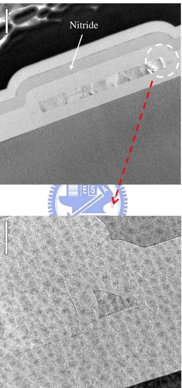
(2) NW-TFTs with Nitride capping layer on mask oxide
The other split was fabricated by Nitride-capping PRTA MILC crystallization. The
seeding window opening. During channel MILC annealing, peak annealing temperature
was individually set at 625°C, 650°C, or 675°C in a rapid thermal processor for 5 or 10
seconds, and off for 30 seconds periodically 60 times, respectively.
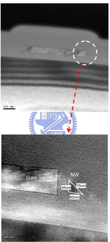
Figure 2-2 illustrates (a) top view of the NW-TFT and (b) the definition of nanowire
width and thickness used. In this experiment, the NW channels were formed by RIE system.
Their feature size is determined by several factors, including height of the side gate, a-Si
thickness, and over-etching time. In this work, the NW channel width and thickness are 45
nm and 60nm, respectively, as shown in the transmission electron microscopy (TEM)
image in Fig. 2-3 and Fig. 2-4. Also note that a parameter called offset, OS, is defined as
the horizontal distance between the MILC open window and the channel. In this study, the
condition for OS is 1 um.
2.2 Measurement Setup and Electrical Characterization
Electrical characterization on the NWFETs was performed using an HP 4156
semiconductor parameter analyzer system. In all measurements, the temperature was
controlled and fixed at a stable value by temperature-regulated hot chuck. From the
measured ID-VG curve at VG = 0.5V, key parameters including threshold voltage (Vth),
following relations.
In this study, a constant-current method was employed to determine the threshold voltage,
in other words, the threshold voltage is defined as the gate voltage as the drain current ID
reaches the value of (W/L)×100 nA, or.
nA L W I V Vth = G@ D = ×100 (2-1),
where W, L are the channel width and length, respectively.
The subthreshold swing could be calculated from the subthrshold current in the weak
inversion region by ) (log D G I V SS ∂ ∂ = (2-2).
Finally, the filed-effect mobility (μFE) is determined by using the following equation:
D ox m FE V WC g L⋅ = μ (2-3),
where gm is the maximum transconductance and Cox is the gate oxide capacitance per unit
Chapter 3
NW-TFTs Fabricated by Pulsed RTA MILC
3.1 Material Analysis of PRTA Grain Growth
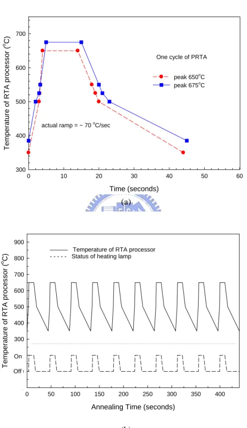
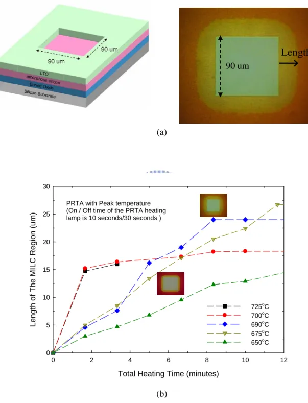
For the material analysis, a 5 nm-thick Ni seeding layer was deposited onto a selected
a-Si region which is called seeding window with dimension of 90×90 μm2.
Recrystallization of the amorphous silicon was subsequently performed to observe the
PRTA MILC characteristics, where all samples were annealed in a RTA processor (AG heat
pulse 610 system) with N2 ambient for 60 cycles with each cycle consisting of 10 seconds
on-period and 30 seconds off-period. Various annealing temperatures, i.e., 650 °C, 675 °C,
690 °C, 700 °C, or 725 °C, were set within every operational cycle. Figure 3-1 illustrates
the heating pattern of the applied temperature which is measured in the chamber during the
annealing process. However, MILC growth rate during cooling interval at 400 °C is less
than 0.1μm/h [48] and can be ignored.
The length of the MILC region formed by PRTA in different annealing conditions is
shown in Fig. 3-2. The value was measured by an optical microscope and was defined as
the length from the center of seeding window edge to the MILC front. Since SPC also
occurs throughout the entire a-Si film during the annealing process, it was observed that the
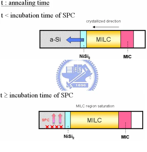
explained by competing crystallization mechanisms between MILC and background solid
phase crystallization. While SPC takes place in the film, the laterally-grown cryststalline
grain is blocked and no further lateral growth is observed. At the onset of the crystallization,
an incubation time is required for the SPC of a-Si to take place. At higher annealing
temperature, the SPC takes place earlier and becomes more dominant than MILC process.
Conversely, the effect of SPC diminishes at low annealing temperature. A distinctive
illustration is depicted in Fig. 3-3. Moreover, the lateral saturation region and film
crystallinity are dependent on the temperature of MILC annealing process. To obtain large
grain size with high quality of film crystallinity, it is necessary to retard the background
SPC process. By properly adjusting the annealing period or the peak temperature
conditions, the PRTA cycle can be tuned to be shorter than the transient time of the
background SPC, the undesirable effect of SPC can thus be completely suppressed during
MILC process [46].
3.2 Activation Energy Extraction
In order to gain a deeper insight into the kinetics of MILC by rapid thermal and furnace
anneal, the activation energy for a-Si to become poly-Si is obtained by thermodynamic
0 exp( )
kT E A
R= ⋅ − a (3-1),
where R is the recrystallization growth rate, A0 is the coefficient constant of growth rate, Ea
is the activation energy, k is the Boltzman constant, and T is the absolute temperature. The
equation can also be expressed as
ln( ) ln( 0) ( )
kT E A
R = + − a (3-2).
The extracted parameters, R and Ea, are related to the different definitions used (some
authors include the incubation time to be part of activation energy calculation), the
apparatuses of annealing, and the preparation of specimens [50]. In this work, the measured
initial rates of MILC crystallization, as a function of annealing temperature are shown in
Fig. 3-4. The activation energy of two dissimilar methods, deduced from the slopes, was
found to be 1.55 eV for PRTA and 1.76 eV for furnace annealing. The lower activation
energy for RTA is believed to be due to photon assisted or free energy released by sudden
heating during RTA [51]. Moreover, the method of PRTA crystallization proceeds much
faster than conventional furnace annealing during MILC process. For instance, the sample
of furnace annealing was prepared at 525 °C for 21 hr to form MILC length of about 32 μm,
whereas the PRTA sample was prepared at 650 °C with 60 cycles of pulses (total heating
time of 10 minutes) to form MILC length of 12.9 μm. Despites the fact that MILC length of
PRTA is shorter than that of furnace annealing, the recrystallized growth rate per unit time
PRTA MILC is also exploited to reduce the long process time in recrystallization.
3.3 Fundamental Characteristics of PRTA NW-TFTs
The operational principles of the novel NW-TFTs are similar to those of the conventional
TFTs. The n+ poly-Si gate is used to modulate the channel potential, consequently
controlling the switching behavior of the devices. Based on one-sided or two-sided seeding
windows for MILC, the NW-TFTs are categorized as metal-induced unilateral
crystallization (MIUC) or metal-induced bilateral crystallization (MIBC). The schematic
device structures of two kinds of MILC seeding windows arrangement are shown in Fig.
3-5, including (a) asymmetric seeding window (ASW), and (b) symmetric seeding window
(SSW). Figure 3-6 presents the growth of MILC region with increasing pulsed cycles, as
observed by optical microscope.
Figure 3-7 shows the transfer characteristics of n-channel NW-TFT devices with ASW
and SSW configurations. The samples were prepared by PRTA anneal at 650 °C peak
temperature with 60 cycles of pulses (total heating time of 10 min) to form MILC
crystallized channel. The performance of ASW devices with different channel lengths are
presented in Fig. 3-7 (a). According to previous material analysis in Section 3.1, MILC
annealing. However, SPC seems to take place earlier than expected. We may exploit the
electrical characteristics to gain insights into the crystalline quality of polysilicon channel.
The result illustrates that the NW crystallinity is dependent on the channel length, i.e., the
NW located near the Ni seeding window depicts superior crystallinity to that away from the
window. It is believed that the heterogeneous nucleation of SPC process, rather than the
Ni-induced lateral recrystallization, dominates the channel recrystallization process in the
area away from the seeding window. Considerable grain boundaries and microstructural
defects in the NW would inevitably degrade the device performance. In addition, along
SiO2 film steps preferential nucleation area during annealing was observed [52]. Since NW
channels are just located at the steps of gate oxide, controlling RTA heating temperature is
supposed to be more significant during MILC treatment. However, for PRTA MILC
technique, NW-TFT devices with SSW has demonstrated that better device performance
can be achieved as shown in Fig. 3-7 (b) and Fig. 3-8, especially in terms of higher drain
current and steeper subthreshold slope, compared with the asymmetric counterparts. It can
be attributed that SSW cases may have more opportunities to develop better NW channel
crystallinity because seeding windows on both the source and drain terminals would
proceed to convert a-Si into polycrystalline silicon simultaneously. The probability of
undesired, fine grains by SPC can be reduced, and the needle-like grain with crystallization
conduction electrons must overcome is also reduced as well. The major device parameters
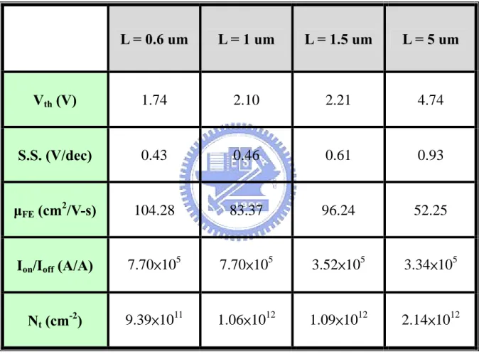
of different channel lengths are extracted and summarized in Table 3-1. Therefore, the
following discussion will focus on NW-TFT devices with SSW configuration. Also noted
that the off-state current of SSW case is rather high due to more Ni residual giving rise to
metal contamination. Further details regarding off-state leakage current mechanisms will be
discussed later.
3.4 Effects of Pulsed RTA Annealing Conditions
3.4.1 Effects of Pulsed RTA Annealing Temperature
In order to obtain ideal crystallinity of NW channels, selecting a precise heating
temperature plays an important role on PRTA MILC fabrication. The MILC annealing
conditions affect not only the recrystallization growth rate but also polycrystalline silicon
grain size, grain boundaries, and even metallic species distribution inside the film. Figure
3-9 compares several MILC annealing splits of n-channel NW-TFTs with an additional
nitride capping layer on the channel. The samples were prepared with different peak PRTA
annealing temperature for 60 cycles. The results show that the three MILC splits (i.e.,
overall channel crystallinity when the channel length is short. When the channel length
increases, the split with polycrystalline silicon formed at 650 °C has better characteristics
in term of steeper subthreshold slope, compared with the other splits of 625 °C and 675 °C.
At higher annealing temperature such as 675 °C, the SPC mechanism of the a-Si layer takes
place quickly and clogs MILC grain growth. Thus, the resultant polycrystalline silicon NW
channel is believed to contain microstructural defects with random crystalline gain
orientation. Besides, the large number of grain boundaries existing in the channel would
degrade the device performance. Another reason of device degradation may relate to Ni
concentration. Higher annealing temperature leads to higher Ni concentration in the MILC
region, grain size decreases due to many NiSi2 crystallites formation during MILC
treatment. This phenomenon, albeit sensitive to annealing temperature, is insensitive to the
annealing time [53]. On the other hand, a relatively low temperature is desirable to form
good-quality MILC polycrystalline channel with larger grain size and less grain boundaries.
However, the MILC of a-Si becomes slower with lower temperature. It will take more time
to achieve the same MILC growth region at lower temperature. The trade-off between the
MILC and SPC should therefore be carefully taken into consideration. Nevertheless,
NW-TFTs without nitride capping layer fabricated by similar MILC annealing conditions
3.4.2 Effects of Pulsed RTA Annealing Time
In the above discussions, the device performance of different PRTA annealing
temperature depends on the channel length of NW-TFTs. For longer channel, the annealing
time is prolonged beyond the incubation time of SPC. Arranging proper annealing period
during each cycle is another approach to suppress SPC mechanism. The samples were
prepared by PRTA anneal periodically for 60 times with 5 seconds per period (i.e., total
heating time of 5 min). The peak temperature was set at 675 °C to make sure that the MILC
recrystallization region is longer than the channel length. The transfer characteristics are
shown in Fig. 3-11, together with those of the sample with the same processing conditions,
except the total heating time of 10 minutes. It can be seen that the device performance is
not improved by reducing the annealing time. It is assumed that MILC lateral-growth
crystallinity does not dominate the entire NW channel. It has been reported by R.B. Iverson
et al. that the incubation time of SPC is roughly 40 minutes in furnace anneal at 675 °C
[54]. While from our material analysis in Section 3.1, the incubation time in RTA anneal at
675°C in our case is about 11 minutes. This suggests that SPC mechanism takes place
earlier in NW channel during PRTA MILC treatment. Thus, PRTA MILC with higher
temperature annealing appears to speed up SPC mechanism and is unfavorable for
3.5 Leakage Mechanisms
The major off-state currents of NW-TFT fabricated by MILC process are related to
several possible paths as depicted in Fig. 3-12. One is through the drain/channel junction
(path 1) and the other is through the gate-to-drain overlap region (path 2). The conduction
mechanisms in the two regions are strongly dependent on the strength of local field which
is determined by the gate and drain biases, referred to as the gate-induced drain leakage
(GIDL). The field-dependent conduction mechanisms are shown in Fig. 3-13. When |VGD|
is high, strong electric field would lead to trap-assisted (Fig.3-13(b)) or band-to-band
tunneling (Fig. 3-13(c)). Major conduction path can be identified by investigating the
dependence of leakage of devices with same channel on the gate-to-drain overlap area [55]:
It is mainly through path 2 as the dependence is linearly proportional to the gate-to-drain
overlap area, and through path 1 as the leakage is independence of the gate-to-drain overlap
area. Typical poly-Si NW devices fabricated in our work follow the path 2 [56]. This is
mainly attributed to the low dopant concentration for the poly-Si layer near the oxide
interface and the relatively low density-of-state (DOS) of the poly-Si film so that the band
bending (related to the electric field) at interface of the poly-Si layer shown in Figs.3-13(b)
and (c) is easy to trigger. To address the issue, we’ve also proposed and demonstrated two
side-gate to reduce the field strength at the channel interface [57]. (2) Promotion of the
dopant concentration in the region of the poly-Si layer near the interface to hinder the
inversion of the drain region (Figs.3-13(b) and (c)) [58]. In one of our previous work, we
also found that, as a poly-SiGe layer is used to replace the poly-SiGe as the NW channel
and the S/D material, the dependence of leakage of devices with same channel is
independent of the gate-to-drain overlap area. This is ascribed to the DOS of the poly-Si
which is much larger than the poly-Si [59]. The high DOS in poly-SiGe would pin the
Fermi level and thus the band-bending is less likely to occur.
For MILC samples, one additional leakage mechanism is attributable to the
contamination of residual Ni. Ni-related species accumulated either at the inter- or
intra-grains may provide more trap states in the band gap of Si, resulting in trap-assisted
tunneling leakage current. Besides, the off-state current of NW-TFT with SSW devices is
more severe. Except the fronts of seeding Ni-silicide from the opposite sides may confront
each other causing metallic species left inside the channel, main reason is one of the
seeding windows located at the gate-to-drain overlap region. Many residual Ni-related
species trap in grain boundaries between the MIC and MILC region. Hence, either forward
or reverse operation modes were used; the leakage currents of SSW devices would be
identical and transfer characteristics are illustrated in Fig. 3-14. Here, the reverse mode of
can be seen if ASW devices operated under reverse mode, owing to the fact that the
Chapter 4
NW-TFTs Fabricated Using Different
Crystallization Strategy
4.1 The Effect of Stress on PRTA NW-TFTs
In this thesis, the effects of capping an additional 100 nm-thick PECVD Nitride film
over the 100 nm LTO layer prior to PRTA MILC treatment on the device characteristics are
studied. Figure 4-1 compares the transfer characteristics of NW-TFT devices with and
without the Nitride-capping layer. We can see that better subthreshold slope and higher
on-current are obtained with the Nitride capping. To study the effect of stress, a 100 nm
LTO and 100 nm Nitride films were deposited on a-Si layer and investigated by stress
measurement. The three layers were all blanket and stacked on a-Si wafer for the test
sample. The stress measurement was performed by probing the change in curvature before
and after the capping of the layer using light interference technique. It was found that a
compressive stress was introduced by nitride film. The measured parameters are listed in
Table 4-1. A compressive stress that exists during phase transformation from a-Si into
poly-Si is believed to be able to suppress the speed of solid phase crystallization owing to
relax causing an increase of strain energy with phase transformation [60]. However, MILC
can still proceed under a compressive stress, since the lateral grain growth is determined by
the free energy difference of Ni atom at the NiSi2/a-Si or NiSi2/c-Si interface. Once the
effect of SPC during lateral grain growth is retarded, improved crystallinity of poly-Si with
less grain boundaries could be carried out during MILC process. The cumulative
probability of NW-TFTs with or without Nitride capping layer was measured and is shown
in Fig. 4-2. It can be seen that performance enhancement is indeed attained.
4.2 The Effect of Crystallization Approaches
4.2.1 Comparisons between Furnace and PRTA Annealing
MILC
For comparison purpose, Fig. 4-3 shows the transfer and output characteristics of MILC
control samples annealed at 525 °C for 21 hr in a conventional furnace. Unlike the samples
fabricated by the PRTA MILC technique as discussed in Chapter 3, NW-TFTs with ASW
configuration exhibit superior device performance to that with SSW configuration. The
extracted field-mobility is 122.4cm2/V-sec for ASW case, which is higher than 88cm2/V-sec
of SSW case. This is interesting as two dissimilar MILC approaches to acquire
and the other by furnace anneal with relatively low temperature but long processing time,
show different trends. The crystallinity of NW is verified to be associated with seeding
window arrangement, crystallization rate, annealing temperature, and annealing time. For
the devices with SSW configuration prepared by conventional MILC furnace anneal,
degraded on-state performance over the asymmetric case has been demonstrated to be
caused by trace amount of metallic species left inside the channel [61]. ASW case depicts
better electrical characteristics in terms of less grain boundaries and less metal
contamination in the channel region. Moreover, throughout the period of furnace annealing,
background SPC mechanism is also triggered as process time increases. When lateral
MILC grain growth is blocked by several small grains formed by SPC, the crystallinity of
NW is affected as well. On the other hand, since higher annealing temperature is exploited
for PRTA MILC technique, the undesired SPC mechanism occurs earlier than expected.
NW channels are crystallized simultaneously by symmetric seeding windows while better
polycrystalline silicon is obtained.
Figure 4-4 shows the transfer and output characteristics of SPC samples annealed at
600 °C for 24 hr in a conventional furnace. Transfer characteristics of MILC (by PRTA and
furnace anneal) and SPC (by furnace anneal) poly-Si TFT with NW channel are compared
in Fig. 4-5. As shown in the figures, two MILC approaches (with SSW configuration)
reduced subthreshold slopes as compared with SPC devices. In addition, the trap density
(Nt) is extracted from the grain boundaries trapping model proposed by J. Levinson et al
[62], defined as ) 8 exp( 2 3 0 G ox s t G ox D D V kTC t N q V C V L W I ε μ − = (4-1)
Where μ0 is a pre-exponential factor, q is the electric charge, Nt is the carrier trap-state
density per unit area, t is the channel thickness, and εs is the semiconductor permittivity. In
Fig. 4-6, the plots of ln(ID/VG) versus (1/VG) for three different approaches of
crystallization are shown, and trap density of each sample is extracted from the
corresponding slope. It can be found that the Nt of MILC devices is much smaller than that
of SPC device. This indicates that NW channel formed by MILC possesses better film
crystallinity. Either furnace or PRTA MILC technique results in much fewer grain
boundaries and microstructural defects in the NW channel. However, rather high off-state
leakage caused by metal contamination is a foremost concern. Finally, the extracted
performance parameters are summarized in Table 4-2.
4.2.2 MILC NW-TFTs with Multiple Channels
Based on the devices structure, the drive current of NW-TFTs is much smaller than that
nano-scale dimension. Boosting the current driving ability can improve the circuit speed
and broaden the practical application of NW-TFTs. Fortunately, the NW channels are
formed simultaneously on the sidewall of poly-Si gate, so NW-TFTs with multiple channels
can be achieved simply by increasing the number of side gates, as depicted in Fig. 4-7.
Figures 4-8 and 4-9 demonstrate the transfer characteristics of NW-TFT with multiple
channels fabricated by furnace and PRTA MILC, respectively. Evidently, the on-current
increase is due to the current sum of all parallel NW channels. The driving ability, however,
is not exactly consistent with the number of multiple channels. Because the crystallinity of
each poly-Si NW is not ideally identical, the variation of transfer characteristics is observed,
as shown Fig. 4-10. When increasing the number of multiple channels, performance
fluctuation of NW-TFTs also becomes larger, as can be seen in Fig. 4-11. In addition, the
off-state leakage current is proportional to the number of channels as well. This is
reasonable since the effective gate-to-drain overlap regions are broadened with increasing
channel number.
4.3 The Fluctuation of NW-TFTs
As device size is scaled below deep-submicrometer regime, the fluctuation of devices
manufacturing process or material-related factors. NW-TFT with MILC crystallized
channel depicts inherent fluctuation which contributes to device performance
non-uniformity. The distribution of metal-induced lateral grains and grain boundaries inside
the NW channel are plausible culprits. In MILC process, the crystallization proceeds
radially from the seeding window. Only lateral grain growth passes through the NW, so the
good quality of crystalline silicon can be achieved. Figure 4-12 compares the cumulative
probability of subthreshold swing and threshold voltage of NW-TFTs fabricated by three
different approaches (i.e., MILC by either PRTA or furnace anneal, and SPC by furnace
anneal). Since SPC nucleates homogeneously within the amorphous film or
heterogeneously on interfaces, small grains are formed randomly in the NW. NW-TFTs by
SPC approach shows the narrowest variation of electrical characteristics among the splits in
Fig. 4-12 which is acceptable as the channel film consists of a large number of small grains.
On the other hand, NW channel crystallized by MILC process in furnace depicts apparently
larger device fluctuation over that by PRTA. As discussed in Chapter 3, the activation
energy of MILC by furnace anneal is higher than that by PRTA, which means that
lateral-crystallization process in furnace is more sensitive to anneal temperature. Light
variation of processing temperature may bring about abnormal MILC growth region, so the
fluctuations of MILC by furnace anneal should be taken into consideration. On the other
annealing temperature. This leads to a smaller fluctuation observed in Fig. 4-12 as
compared with the MILC samples prepared by furnace. Moreover, a fast crystallization rate
by using PRTA MILC is believed to be capable of eliminating the fluctuation of NW-TFT
device performance, since the annealing time in crystallizing is substantially reduced in
contrast to MILC by furnace-anneal. Therefore, MILC process fabricated by PRTA
technique is promising as it not only reduces process time in crystallization which is
Chapter 5
Conclusions and Future Work
5.1 Conclusions
In this thesis, a novel MILC technique using pulsed-RTA to crystallize NW channel is
studied. Our results indicate that PRTA MILC has a faster recrystallized growth rate than
that of conventional furnace anneal owing to higher crystallization temperature and lower
activation energy. The effects of PRTA annealing condition were also investigated as well.
The crystallinity of NW is explained by competing crystallization mechanisms between
MILC and SPC. Specifically, undesired SPC mechanism of the a-Si layer takes place
quickly and clogs MILC grain growth at higher annealing temperature. A lower
temperature is preferred to form good-quality of laterally-grown cryststalline grain,
however, the MILC of a-Si becomes slower with lower annealing temperature. The
trade-off between the MILC and SPC should therefore be carefully taken into
consideration.
The effect of additional stress on the NW channel is studied to improve MILC device
characteristics because it is capable of suppressing the speed of background solid phase
crystallization. We have also fabricated and characterized devices with multiple NW
the channel number increases. Moreover, the NW channels crystallized by MILC process in
furnace depict apparently wider device fluctuation than those by PRTA. Abnormal MILC
growth region may result in crystallinity difference in each poly-Si NW. MILC process
fabricated by PRTA technique, however, appears to be a promising approach as it not only
reduces process time in crystallizing which is suitable for mass-production, but also
achieves better uniformity in device characteristics.
5.2 Future Work
The development and characterization of NW-TFTs with PRTA and furnace annealing
MILC channels have been studied in this thesis. To further enhance the device performance,
several propositions are suggested for future work.
1. Through the post-treatments like high temperature annealing and hydrogenation
plasma passivation, further improvement in electrical performance is expected by
enlarging the grain size and eliminating defects in the MILC film.
2. Several reports have revealed that the growth rate of MILC can be enhanced by
incorporation of boron into a-Si channel (i.e., dopant effect of MILC) [63]. For
NW through additional BF2+ implantation.
3. Both MILC and SPC techniques have been studied in fabricating NW-TFTs. Another
interesting approach in the preparation of LTPS film, excimer laser annealing (ELA),
References
[1] S. D. Brotherton, “Polycrystalline Silicon Thin Film Transistors,” Semicond. Sci.
Technol., vol. 10, pp. 721-738, 1995.
[2] A. G. Lewis, D. D. Lee and R. H. Bruce, “Polysilicon TFT Circuit Design and Performance,” IEEE J. Solid-State Circuits, vol. 27, pp. 1833-1842, 1992.
[3] A. Mimura, N. Konishi, K. Ono, J. I. Ohwada, Y. Hosokawa, Y. A. Ono, T. Suzuki, K. Miyata and H. Kawakami, “High Performance Low-temperature Poly-Si n-channel TFT’s for LCD,” IEEE Trans. Electron Devices, vol. 36, pp. 351-359, 1989.
[4] S. W. Lee and S. K. Joo, “Low Temperature Poly-Si Thin-film Transistor Fabrication by Metal-induced Lateral Crystallization,” IEEE Electron Device Lett., vol. 17, pp. 160-162, 1996.
[5] T. Sameshima, M. Hara and S. Usui, “XeCl Excimer Laser Annealing Used to Fabricate Poly-Si TFT’s,” Jpn. J. Appl. Phys., vol. 28, pp. 1789-1793, 1989.
[6] G. Shi and J. H. Seinfeld, “Transient Kinetics of Nucleation and Crystallization: Part I. Nucleation,” J. Mater. Res., vol. 6, pp. 2091-2096, 1991.
[7] G. Shi, J. H. Seinfeld, “Transient Kinetics of Nucleation and Crystallization: Part II. Nucleation,” J. Mater. Res., vol. 6, pp. 2097-2102, 1991.
[8] Y. Masaki, P. G. LeComber and A. G. Fitzgerald, “Solid Phase Crystallization of Thin Films of Si Prepared by Plasma-enhanced Chemical Vapor Deposition,” J. Appl. Phys. vol. 74, pp. 129-134, 1993.
[9] H. C. Cheng, F. S. Wang and C. Y. Huang, “Effects of NH3 Plasma Passivation on n-channel Polycrystalline Silicon Thin-film Transistors,” IEEE Trans. Electron
Devices, vol. 44, pp. 64-68, 1997.
Electron Device Lett., vol. 10, pp. 123-125, 1989.
[11] H. N. Chern, C. L. Lee and T. F. Lei, “The Effects of H2-O2-plasma Treatment on The Characteristics of Polysilicon Thin-film Transistors,” IEEE Trans. Electron Devices, vol. 40, pp. 2301-2306, 1993.
[12] U. Mitra, B. Rossi, and B. Khan, “Mechanism of Plasma Hydrogenation of Polysilicon Thin Film Transistors,” J. Electrochem. Soc., vol. 138, pp. 3420-3424, 1991.
[13] K. Shimizu, O. Sugiura and M. Matsumura, “High-mobility Poly-Si Thin-film Transistors Fabricated by a Novel Excimer Laser Crystallization Method,” IEEE
Trans. Electron Devices, vol. 40, pp. 112-117, 1993.
[14] M. Yasushi and N. Takashi, “UV Pulsed Laser Annealing of Si+ Implanted Silicon Film and Low-temperature Super-thin Film Transistors,” Jpn. J. Appl. Phys., vol. 28, pp. 309-311, 1989.
[15] K. Mutsumi, I. Satoshi and S. Tatsuya, “Dependence of Polycrystalline Silicon Thin-film Transistor Characteristics on the Grain-boundary Location,” Appl. Phys., vol. 89, pp. 596-600, 2001.
[16] R. S. Sposili and J. S. Im, “Sequential Lateral Solidification of Thin Silicon Films on SiO2,” Appl. Phys. Lett., vol. 69, pp. 2864-2866, 1996.
[17] P. C. Wilt, B. D. Dijk, G. J. Bertens, R. Ishihara and C. I. Beenakker, “Formation of Location-controlled Crystalline Islands Using Substrate-embedded Seeds in Excimer-laser Crystallization of Silicon Films,” Appl. Phys. Lett., vol. 79, pp. 1819-1821, 2001.
[18] C. H. Oh, M. Ozawa and M. Matsumura, “A Novel Phase-Modulated Excimer-laser Crystallization Method of Silicon Thin Films,” Jpn. J. Appl. Phys., vol.37, pp. 492-495, 1998.
Y. Sano and N. Sasaki, “High Performance Low Temperature Polycrystalline Silicon Thin Film Transistors on Non-alkaline Glass Produced Using Diode Pumped Solid State Continuous Wave Laser Lateral Crystallization,” Jpn. J. Appl Phys., vol. 43, pp. 1269-1276, 2004.
[20] M. Tai, M. Hatano, S. Yamaguchi, T. Noda, S. K. Park, T. Shiba and M. Ohkura, “Performance of Poly-Si TFTs Fabricated by SELAX,” IEEE Trans. Electron Devices, vol. 51, pp. 934-939, 2004.
[21] G. Radnoczi, A. Robertsson, H. T. Hentzell, S. F. Gong and M. A. Hasan, “Al Induced Crystallization of a-Si,” J. Appl. Phys., vol. 69, pp. 6394-6399, 1991.
[22] L. Hultman, A. Robertsson, H. T. Hentzell, I. Engström and P. A. Psaras, “Crystallization of Amorphous Silicon During Thin-film Gold Reaction,” J. Appl.
Phys., vol. 62, pp. 3647-3655, 1987.
[23] S. F. Gong, H. T. Hentzell and A. E. Robertsson, “Initial Solid-state Reactions between Crystalline Sb and Amorphous Si Thin Films,” J. Appl. Phys., vol. 64, pp. 1457-1463, 1988.
[24] R. J. Nemanichi, R. T. Fulks, B. L. Stafford and H. A. Plas, “Initial reactions and Silicide Formation of Titanium on Silicon Studied by Raman Spectroscopy,” J. Vac.
Sci. Technol. A, vol. 3, pp. 938-941, 1985.
[25] S. W. Lee, Y. C. Jeon and S. Ki. Joo, “Pd Induced Lateral Crystallization of Amorphous Si Thin Films,” Appl. Phys. Lett., vol. 66, pp. 1671-1673, 1995.
[26] S. W. Lee and S. K. Joo, “Low Temperature Poly-Si Thin-film Transistor Fabrication by Metal-induced Lateral Crystallization,” IEEE Electron Device Lett., vol. 17, pp. 160-162, 1996.
[27] Y. G. Yoon, M. S. Kim, G. B. Kim and S. K. Joo, “Metal-induced Lateral Crystallization of a-Si Thin Films by Ni-Co Alloys and the Electrical Properties of
[28] M. Wang, Z. Meng and M. Wong, “The Effects of High Temperature Annealing on Metal-induced Laterally Crystallized Polycrystalline Silicon,” IEEE Trans. Electron
Devices, vol. 47, pp. 2061-2067, 2000.
[29] C. Hayzelden and J. L. Batstone, “Silicide Formation and Silicide-mediated Crystallization of Nickel-implanted Amorphous Silicon Thin Films,” J. Appl. Phys., vol. 73, pp. 8279-8289, 1993.
[30] F. L. Yang, D. H. Lee, H. Y. Chen, C. Y. Chang, S. D. Liu and C. C. Huang, “5 nm-gate Nanowire FinFET,” VLSI Symp. Tech. Dig., pp. 196-197, 2004.
[31] X. Duan., Y. Huang and C. M. Lieber, “Nonvolatile Memory and Programmable Logic From Molecule-gated Nanowires,” Nano Lett., vol. 2, pp. 497-490, 2002.
[32] X. Duan, C. Niu, V. Sahi, J. Chen, J. W. Parce, S. Empedocles and J. L. Goldman, “High-performance Thin-film Transistors Using Semiconductor Nanowires and Nanoribbons,” Nature, vol. 425, pp. 274-278, 2003.
[33] Q. Wei, H. Park and C. M. Lieber, “Nanowire nanosensors for Highly Sensitive and Selective Detection of Biological and Chemical Species,” Science, vol. 293, no. 5533, pp. 1289-1292, 2001.
[34] Z. Li, Y. Chen, X. Li, T. Kamins, K. Nauka and R. S. Williams, "Sequence-specific Label-free DNA Sensors Based on Silicon Nanowires," Nano Lett., vol. 4, no. 2, pp. 245-247, 2004.
[35] M. C. McAlpine, R. S. Friedman, S. Jin, K. H. Lin, W. U. Wang and C. M. Lieber, “High-performance Nanowire Electronics and Photonics on Glass and Plastic Substrates,” Nano Lett., vol. 3, pp. 1531-1535, 2003.
[36] X. Duan and C. M. Lieber, “Laser-assisted Catalytic Growth of Single Crystal GaN Nanowires,” J. of American Chemical Society, vol.122, pp.188-189, 2000.
[37] X. Duan, Y. Huang, Y. Cui, J. Wang and C. M. Lieber, “Indium Phosphide Nanowires as Building Blocks for Nanoscale Electronic and Optoelectronic Devices,” Nature, vol.
409, pp.66-69, 2001.
[38] Y. Huang, X. Duan, Q. Wei and C. M. Lieber, “Directed Assembly of One-dimensional Nanostructures into Functional Networks,” Science, vol. 291, pp. 630-633, 2001.
[39] A. Tao, F. Kim, C. Hess, J. Goldberger, R. He, Y. Sun, Y. Xia and P. Yang, “Langmuir-Blodgett Silver Nanowire Monolayers for Molecular Sensing Using Surface-enhanced Raman Spectroscopy,” Nano Lett., vol. 3, pp. 1229-1233, 2003. [40] S. J. Tans, R. M. Verschueren and C. Dekker, “Room-temperature Transistor Based on
a Single Carbon Nanotube,” Nature, vol. 393, pp. 49-52, 1998.
[41] M. S. Fuhrer, J. Nygard, L. Shih, M. Forero, Y. G. Yoon, M. S. Mazzoni, H. J. Choi, J. Ihm, S. G. Louie, A. Zettl and P. L. McEuen, “Crossed Nanotube Junctions,” Science, vol. 288, no. 5465, pp. 494-497, 2000.
[42] M. D. Austin, H. Ge, W. Wu, M. Li, Z. Yu, D. Wasserman, S. A. Lyon and S. Y. Chou, “Fabrication of 5 nm Linewidth and 14 nm Pitch Features by Nanoimprint Lithography,” Appl. Phys. Lett., vol. 84, pp. 5299-5301, 2004.
[43] Y. K. Choi, T. J. King and C. Hu, “A Spacer Patterning Technology for Nanoscale CMOS,” IEEE Trans. Electron Devices, vol. 49, pp. 436-441, 2002.
[44] H. Wang, M. Chan, S. Jagar, V. M. Poon, M. Qin, Y. Wang and P. K. Ko, “Super Thin-film Transistor with SOI CMOS Performance Formed by a Novel Grain Enhancement Method,” IEEE Trans. Electron Devices, vol. 47, pp. 1580-1586, 2000. [45] V. W. Chan, P. C. Chan and M. Chan, “Three Dimensional CMOS Integrated Circuits
on Large Grain Polysilicon Films,” IEDM Tech. Dig., pp. 161-164, 2000.
[46] C. F. Cheng, T. C. Leung, M. C. Poon and M. Chan, “Large-Grain Polysilicon Crystallization Enhancement Using Pulsed RTA”, IEEE Electron Device Lett., vol. 25, pp. 553-555, 2004.
Low-cost Method to Fabricate TFTs with Poly-Si Nanowire Channel,” IEEE Electron
Device Lett., vol. 26, pp. 643-645, 2005.
[48] M. Wong, Z. Jin, G. A. Bhat, P. C. Wong and H. S. Kwok, "Characterization of the MIC/MILC Interface and Its Effects on the Performance of MILC Thin-film Transistor," IEEE Trans. Electron Devices, vol. 47, pp. 1061-1067, 2000.
[49] K. H. Kim, W. S. Sohn, J. H. Oh, S. J. Park, J. Jang and S. H. Kang, “Crystallization Temperature Dependence of Electrical Conductivity on SMC Poly-Si,” J. of Korean
Phys. Soc., vol.42, pp.462-465, 2003.
[50] L. K. Lam, S. Chen and D. G.. Ast, “Kinetics of Nickel-induced Lateral Crystallization of Amorphous Silicon Thin-film Transistors by Rapid Thermal and Furnace Anneals,”
Appl. Phys. Lett., vol. 74, pp. 1866-1868, 1999.
[51] R. Kingi, Y. Wang, S. J. Fonash, O. Awadelkarim, J. Mehlhaff and H. Hovagimian, “Comparison between Rapid Thermal and Furnace Annealing for a-Si Solid Phase Crystallization,” Mater. Res. Soc. Symp. Proc., vol. 424, pp. 237-241, 1997.
[52] M. Moniwa, M. Miyao, R. Tsuchiyama, A. Ishizaka, H. Sunami, M. Ichikawa and T. Tokuyama, “Preferential Nucleation along SiO2 Steps in Amorphous Si,” Appl. Phys.
Lett., vol. 47, pp. 113-115, 1985.
[53] C. F. Cheng, M. C. Poon, C. W. Kok and M. Chan, “Modeling of Metal-induced-lateral-crystallization Mechanism for Optimization of High Performance Thin-film-transistor Fabrication,” IEDM Tech. Dig., pp. 569-572, 2002. [54] R. B. Iverson and R. Reif, “Recrystallization of Amorphized Polycrystalline Silicon
Films on SiO2: Temperature Dependence of the Crystallization Parameters,” J. Appl. Phys., vol. 62, pp.1675-1681, 1987.
[55] K. Roy, S. Mukhopadhyay and H. Mahmoodi-Meimand, “Leakage Current Mechanisms and Leakage Reduction Techniques in Deep-submicrometer CMOS Circuits,” Proceedings of the IEEE, vol. 91, pp. 305-327, 2003.
[56] H. C. Lin, M. H. Lee, C. J. Su and S. W. Shen, “Fabrication and Characterization of Nanowire Transistors with Solid-phase Crystallized Poly-Si Channels,” IEEE Trans.
Electron Devices, vol. 53, pp. 2471-2477, 2006.
[57] H. H. Tsai, H. C. Lin and T. Y. Huang, “Performance Enhancement in Thin-Film Transistors with Poly-Si Nanowire Channels,” Master thesis, Institute of Electronics Engineering, National Chiao Tung University, 2006.
[58] Y. F. Huang, H. C. Lin and T. Y. Huang, “A Study of Thin-Film Transistors with Poly-Si Nanowire Channels Fabricated by LTPS Technology,” Master thesis, Institute of Electronics Engineering, National Chiao Tung University, 2007.
[59] M. H. Lee, H. C. Lin and T. Y. Huang, “A Study of Leakage Current and Reliability Issues in Poly-Si Thin Film Transistors,” Ph.D. dissertation, Institute of Electronics Engineering, National Chiao Tung University, 2007.
[60] Y. Kimura, M. Kishi and T. Katoda, “Effects Of Elastic Stress Introduced By A Silicon Nitride Cap On Solid-phase Crystallization Of Amorphous Silicon,” J. Appl. Phys., vol. 86, pp. 2278-2280, 1999.
[61] H. C. Lin and C. J. Su, ” High-Performance Poly-Si Nanowire NMOS Transistors,” IEEE Trans. on Nanotechnology, vol. 6, pp. 206-212, 2007.
[62] J. Levinson, F. R. Shepherd, P. J. Scanlon, W. D. Westwood, G. Este and M. Rider, “Conductivity Behavior In Polycrystalline Semiconductor Thin Film Transistors,” J.
Appl. Phys., vol. 53, pp. 1193-1202, 1982.
[63] T. Ma and M. Wong, “Dopant And Thickness Dependence Of Metal-induced Lateral Crystallization Of Amorphous Silicon Films,” J. Appl. Phys., vol. 91, pp. 1236-1241, 2002.
Table 1-1 The comparisons among SPC, ELA, and MILC.
MILC
SPC
ELA
Conventional
PRTA
Temperature
High Low
Medium
Medium/High
Time
Long Short Medium Short
Grain size
Small Medium Large
Large/Medium
Cost
Low High Low Low
Throughput
Batch Single Batch Single
Table 3-1 Key electrical parameters of NW-TFTs with SSW configuration by PRTA MILC.
L = 0.6 um
L = 1 um
L = 1.5 um
L = 5 um
V
th(V)
1.74 2.10 2.21 4.74
S.S. (V/dec)
0.43 0.46 0.61 0.93
μ
FE(cm
2/V-s)
104.28 83.37 96.24 52.25
I
on/I
off(A/A)
7.70×10
57.70×10
53.52×10
53.34×10
5N
t(cm
-2)
9.39×10
111.06×10
121.09×10
122.14×10
12* All parameters were extracted at VD = 0.5 V except for the off-state current, Ioff , and on/off current ratio, Ion/Ioff , which were extracted at VD = 3 V.