國立交通大學
電機學院 電子與光電學程
碩 士 論 文
應用於視訊系統之高頻率倍數全數位式鎖相迴路時脈
產生器
An ADPLL Clock Generator with Large Frequency
Multiplication Factor for Video Application
研 究 生 : 黃文明
指導教授 : 李鎮宜 教授
應用於視訊系統之高頻率倍數全數位式鎖相迴路時脈
產生器
An ADPLL Clock Generator with Large Frequency
Multiplication Factor for Video Application
研 究 生:黃文明 Student:Wen-Ming Huang
指導教授:李鎮宜 Advisor:Chen-Yi Lee
國 立 交 通 大 學
電機學院 電子與光電學程
碩 士 論 文
A ThesisSubmitted to College of Electrical and Computer Engineering National Chiao Tung University
in partial Fulfillment of the Requirements for the Degree of
Master of Science in
Electronics and Electro-Optical Engineering June 2007
Hsinchu, Taiwan, Republic of China
應用於視訊系統之高頻率倍數全數位式鎖相迴路時脈
產生器
研究生:黃文明 指導教授:李鎮宜 教授
國立交通大學
電機學院 電子與光電學程
摘要
在本論文中,我們提出一個高頻率倍數的全數位式鎖相迴路,此電路可應用 於視訊系統中的時脈產生器,其主要功能是接收顯示卡發出的水平同步訊號,並 依據使用者設定的螢幕解析度,產生高頻像素時脈來擷取視訊訊號資料,取樣點 的穩定度直接影響到顯示畫面的品質,若是像素時脈不穩定,則顯示畫面會閃爍 或抖動。因此,如何在高頻率倍數下,產生一個穩定的時脈訊號,是此電路設計 的重點。我們使用標準元件庫來設計整個晶片,並利用合成軟體及自動佈局工具 實現電路,最後以 90 奈米 1P9M 標準 CMOS 製程來製作晶片。An ADPLL Clock Generator with Large Frequency
Multiplication Factor for Video Application
Student:Wen-Ming Huang Advisor:Dr. Chen-Yi Lee
Degree Program of Electrical and Computer Engineering
National Chiao Tung University
Abstract
In this thesis, an all-digital phase-locked loop with large multiplication factor is presented. This circuit can be applied to the video system as a clock generator. It receives the horizontal synchronous signal from the graphics card and then generates a high frequency pixel clock according to the monitor resolution setting to acquire the video signal data. The stability of this sampling clock affects the display image quality directly. If the pixel clock is not stable, the display image will be glittering or jittering. Therefore, how to design a stable clock generator with large multiplication factor is the point of this thesis. This chip is implemented with standard cell library by synthesis and auto place-and-route tools, and realized using 90nm 1P9M standard CMOS process.
Acknowledgements
I would like to express my immense gratitude to my advisor Prof. Chen-Yi Lee for his enthusiastic guidance and encouragement throughout the research, and give him and his family my sincere wishes.
I want to thank all my Si2 group mates, especially Dr. Ching-Che Chung, for many fruitful discussions and valuable suggestions. I could not complete my study without their help. I also want to thank anyone who ever helped me in the past.
Finally, I would like to give the greatest respect and love to my family and my girlfriend. I deeply appreciate their support and understanding these days.
Contents
Chapter 1 Introduction 6
1.1 Motivation 6
1.2 Thesis Organization 8
Chapter 2 Overview of Video System and Line-Locked PLL 9
2.1 Video System Basics 9
2.1.1 Video Display System Structure 9
2.1.2 Video Synchronous Signal Timing Definition 11
2.1.3 Monitor Timing Specification 12
2.2 Line-Locked PLL Overview 14
2.2.1 A Survey of Line-Locked PLL 14
2.2.2 A Survey of Large Multiplication Factor PLL 17
2.2.3 Summary 20
2.3 Design Challenge 21
2.3.1 The Difficulty of Large Multiplication Factor PLL Design 21
2.3.2 The Effect of Cycle Slipping Phenomenon 23
2.3.3 The Impact of Hsync Jitter Injection 26
Chapter 3 ADPLL Clock Generator Circuit Design 27
3.1 The Proposed ADPLL Architecture 27
3.2 Phase/Frequency Detector 29
3.3 Digital-Controlled Oscillator 31
3.5.1 State Diagram of Control Unit 36
3.5.2 Timing Diagram of Control Unit 39
Chapter 4 Chip Implementation 45
4.1 Chip Layout 45
4.2 Circuit Simulation Result 45
4.3 Chip Measurement Result 47
Chapter 5 Conclusion and Future Work 50
Reference 51
List of Figures
Fig. 1.1. A typical PLL block diagram 6
Fig. 2.1. A brief video display system diagram [14] 10
Fig. 2.2. Video signal and sampling clock timing diagram 10
Fig. 2.3. Video synchronous signal timing definition 11
Fig. 2.4. Monitor display area 11
Fig. 2.5. Separate Vsync/Hsync signal and pixel clock timing diagram 12
Fig. 2.6. Video line-locked PLL block diagram [22] 14
Fig. 2.7. Control mode flow chart [22] 15
Fig. 2.8. Video capture PLL [23] 16
Fig. 2.9. Low refresh rate PLL [24] 17
Fig. 2.10. A large frequency multiplication factor PLL [26] 18
Fig. 2.11. A 4 to 1022 multiplication factor PLL [27] 19
Fig. 2.12. A 1 to 4096 multiplication factor PLL [28] 20
Fig. 2.13. A tracking jitter problem of large multiplication factor 22
Fig. 2.14. Jitter versus multiplication factor at fixed 240 MHz output [28] 22
Fig. 2.15. The impact of cycle slipping on lock time 23
Fig. 2.16. (a) Conventional three-state phase detector architecture 24
(b) State diagram of the three-state phase detector Fig. 2.17. (a) Ideal linear PFD characteristic 25
(b) Nonideal linear PFD characteristic Fig. 2.18. PFD nonideal behavior due to nonzero reset path delay 25
Fig. 3.1. The proposed ADPLL clock generator architecture 28
Fig. 3.2. The simulation waveform of the proposed ADPLL 28
Fig. 3.3. The schematic of the proposed PFD 29
Fig. 3.5. The simulation result of the proposed PFD 30
Fig. 3.6. The schematic of the proposed DCO 31
Fig. 3.7. The schematic of the proposed SAR tuning stage 32
Fig. 3.8. The schematic of the proposed linear tuning stage 33
Fig. 3.9. The schematic of the proposed DCO dithering stages 34
Fig. 3.10. The schematic of the proposed phase adjustment circuit 35
Fig. 3.11. The state diagram of the control unit 36
Fig. 3.12. The timing diagram of DCO dithering method 38
Fig. 3.13. The timing diagram of control unit 39
Fig. 3.14. The timing diagram of SAR frequency search state 41
Fig. 3.15. The timing diagram of LIN frequency search state 42
Fig. 3.16. The timing diagram of DIT1 frequency search state 43
Fig. 3.17. The timing diagram of DIT2 phase tracking state 44
Fig. 4.1. The ADPLL core circuit layout 45
Fig. 4.2. Mixed-mode simulation environment 47
Fig. 4.3. The ADPLL functional test waveform 47
Fig. 4.4. Pixel clock measurement result 48
Fig. 4.5. Phase difference measurement result 48
List of Tables
Table 2.1. Monitor timing specification 13
Table 2.2. Some design problems of early PLL publications 20
Table 3.1. The tuning range simulation result of the SAR stage 32
Table 3.2. The tuning range simulation result of the linear stage 33
Table 3.3. The tuning range simulation result of the DCO dithering stages 34
Table 3.4. The simulation result of the overall DCO operation range 34
Table 3.5. The simulation result of the proposed phase adjustment circuit 35
Table 4.1. The proposed DCO simulation result 46
Table 4.2. The proposed adjustment circuit simulation result 46
Table 4.3. The proposed ADPLL full chip simulation result 47
Chapter 1
Introduction
1.1 Motivation
Since the first phase-locked loops (PLL) were realized with discrete components, they are integrated in a monolithic chip nowadays. The PLLs have been widely used as clock generators in electronic systems, such as microprocessors, system-on-chip (SoC) applications, data communication systems, and so forth [1-13] in the past decades. A PLL is a circuit that synchronizes an output signal with a reference or input signal in frequency as well as in phase, i.e. a PLL circuit causes a particular system to track with another one. A typical PLL block diagram is illustrated in Fig. 1.1. It consists of five fundamental blocks: a phase-frequency detector (PFD), a charge pump (CP), a loop filter (LF), a voltage-controlled oscillator (VCO), and clock divider. The frequency of the output clock is N times of the input clock. Generally, a PLL-based clock generator receives a low frequency input clock as a reference signal, which commonly comes from a quartz oscillator, and generates a high frequency signal according to a specific multiplication factor. This frequency multiplication factor of the PLLs usually ranges from several tens to several hundreds in microprocessor or data communication system applications.
Another important application of PLLs is the pixel clock generator, so-called line-locked PLL or video capture PLL, in the graphics or video display system [14-25]. This kind of PLL receives a low frequency horizontal synchronous signal from the graphics card and generates a high frequency pixel clock according to the display resolution for sampling the video signals. The frequency multiple between the input horizontal synchronous signal and the output pixel clock is quite large; it ranges from several hundreds to several thousands depending on the image resolution of the display system. The higher the image resolution, the larger the frequency multiple. As we know, the loop stability and output jitter would be thorny problems in the large frequency multiplication factor PLL circuit design. Besides the large frequency multiplication factor, the phase synchronization between the horizontal synchronous signal and the pixel clock is another chief design consideration. Since the period of the horizontal synchronous signal represents the time interval of one horizontal scan line on the screen, the generated pixel clock must be synchronized to it. If their phases are not well aligned, the images on the screen will appear distorted.
As the progressing of modern display technology, the video image quality is becoming better and better. The image resolution of the display system increases rapidly. The proposed PLL circuit is a large multiplication factor line-locked PLL for video application. We aim to design a pixel clock generator that can be accommodated to the current monitor timing specifications [57]. The proposed PLL circuit is achieved by means of cell-based all-digital approach [9-13]. The cell-based all-digital approach benefits in many ways: easy portability for different processes, high integration in SoC design, good immunity against switching noise and leakage, and low barrier in low voltage design. This chip is implemented in a 90nm 1p9m 1.0v/2.5v standard CMOS process. The total gate count is 2.4K, and the core circuit size is 100x100um2.
1.2 Thesis Organization
This thesis is arranged as follows. In chapter 2, we introduce the basic structure and timing definition of the video display system. A survey and the design challenges of the line-locked PLL are also described. In chapter 3, all the details of the proposed ADPLL clock generator, including the circuit architecture, functional blocks, and control algorithm, are presented. The chip implement, simulation, and measurement results are reported in chapter 4. Finally, we make conclusions and point out several design issues that need to be explored in the future in chapter 5.
Chapter 2
Overview of Video System and
Line-Locked PLL
2.1 Video System Basics
The video display system structure, video signal timing definition, and monitor timing specification are presented in this section.
2.1.1 Video Display System Structure
A brief video display system diagram [14] is shown in Fig. 2.1. The essential Red/Green/Blue (RGB) video signals are delivered along with vertical synchronous (Vsync) and horizontal synchronous (Hsync) signals by random access memory digital-analog converter (RAMDAC) of the computer. The main function of the RGB acquisition interface is to convert the analog video signals into digital signals through variable gain amplifier (VGA) and analog-to-digital converter (ADC). The sampling clock of the ADC comes from a clock generator, usually a PLL. This clock generator receives low frequency Hsync from computer and produces high frequency pixel clock according to the screen resolution of the display system. In other words, the pixel frequency is determined by the input Hsync frequency and the horizontal resolution. This pixel clock acts as sampling clock for converting the analog video signals into digital signals. The digital video signals are sent to digital processor and then transmitted to the display system. The multiple between Hsync and pixel clock is proportional to the screen horizontal resolution. Many popular monitor timing specification have been established by video electronics standards association
(VESA). A finer image quality has a higher screen resolution. Take one of the XGA mode as an example, the Hsync frequency is 48.4 KHz while the pixel frequency is 65.0 MHz. The pixel clock is 1344 times the frequency of the Hsync signal. Therefore, the frequency multiplication factor of the clock generator is 1344.
Fig. 2.1. A brief video display system diagram [14]
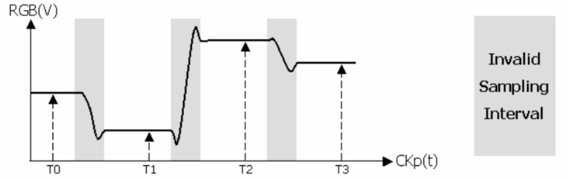
The stability of this sampling clock plays an important role to the display system performance. The video signal and sampling clock timing diagram [14,16,18,20,25] is shown in Fig. 2.2. The only valid sampling duration is the portion when video signal is stable. On the contrary, the signal transition region is invalid sampling interval. Once the sampling point locates in the invalid intervals, the acquired video data would be corrupted. Consequently, the image on the display screen will be distorted.
2.1.2 Video Synchronous Signal Timing Definition
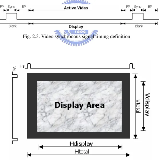
The video synchronous signal timing definition [57] is shown in Fig. 2.3. The video synchronous signal is composed of synchronous pulse (Sync), front porch (FP), back porch (BP) and active video subsections. The period of vertical synchronous signal defines the time interval of a display frame, i.e. the refresh time between two images. The period of horizontal synchronous signal defines the time interval of a scan line. The screen is blank from the start of front porch to the end of back porch. The image pattern only displays on the screen during the active video period. From these definitions, we know that the monitor display area is only the central active part of the screen as shown in Fig. 2.4.
Fig. 2.3. Video synchronous signal timing definition
Now, taking a closer look at the synchronous signals and the pixel clock. For an MxN display resolution, where M means the active horizontal resolution and N means the active vertical resolution, the period of Vsync is N times of Hsync while the period of Hsync is M times of pixel clock. That is to say, in the active display area, there are N horizontal scan lines in one display frame and there are M pixels in one horizontal scan line in case of an MxN display resolution. The more detail timing diagram [18,19,57] is shown in Fig. 2.5.
Fig. 2.5. Separate Vsync/Hsync signal and pixel clock timing diagram
2.1.3 Monitor Timing Specification
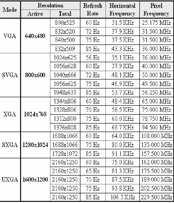
Many industrial standards of monitor timing specification have been developed by VESA for a long time. The most popular display modes are VGA (Video Graphics
Array), SVGA (Super Video Graphics Array), XGA (Extended Graphics Array), SXGA (Super Extended Graphics Array), and UXGA (Ultra Extended Graphics Array). The monitor timing specifications [57] of these modes are listed in Table 2.1.
The active resolution defines the displayed horizontal and vertical ranges, while the total resolution includes the blank area. It is worthy of noticing that the frequency multiple relation between Hsync and pixel clock is the total horizontal resolution not the active one. For instance, the pixel clock is 800 times the frequency of the Hsync instead of 640 times in the 60 Hz refresh rate 640x480 resolution VGA mode.
2.2 Line-Locked PLL Overview
The so-called line-locked or video capture PLL is a clock generator employed in the video acquisition interface that generates a pixel clock, which is phased-locked with the horizontal synchronous signal as mentioned in the previous section. The large frequency multiplication factor of this kind PLL is inherent in the video display system. We will deliver several line-locked and large multiplication factor PLL examples briefly and make a summary of this section.
2.2.1 A Survey of Line-Locked PLL
The first video line-locked PLL [22] example is illustrated in Fig. 2.6. This PLL is composed of phase detector, frequency detector, charge pump, VCO, clock divider, and control unit. The control mode flow chart of this circuit is shown in Fig. 2.7. The control unit operates in conjunction with phase detector and frequency detector to provide one of five modes of operation: coarse frequency (CFR), fine frequency (FFR), coarse phase (CPH), fine phase (FPH), or hold (HOLD). It needs an external RC as loop filter.
Starting from an out-of-lock condition with a large frequency error, the PLL goes into the CFR mode where frequency error is adjusted in approximately ±4% steps. After stepping the clock frequency within 4% of that desired, the PLL goes into the FFR mode. When the clock frequency is around 2% of that desired, the PLL goes into CPH mode. Finally, when the phase error is within 2 clock periods, the PLL goes into FPH mode. If the input HSRef signal disappears, the PLL goes into the HOLD mode and the VCO control voltage is held fixed until HSRef is restored. In additional, the ÷N counter divides the clock frequency by Nset and outputs ClkDiv pulse. The decimal value of Nset is expected to be between 750 and 2600. There is provision for resetting the phase of ClkDiv to align with HSRef by means of reset pulse Reset generated in CPH mode.
The second example is video capture PLL by Analog Bits Inc. [23]. This PLL circuit is composed of phase/frequency detector, numeric-controlled oscillator, phase interpolator, clock divider, control unit, and two internal PLLs. An internal PLL generates a 5-phase 660MHz clock from a 14.3MHz system reference clock as a high precision time reference. The PLL utilizes a high precision 28-bit digital frequency synthesizer, with a programmable all-digital loop filter making it possible to generate an output clock with less jitter. A 12-bit clock divider can accomplish the frequency multiplication. A controllable fine phase delay line is inserted in the output path for external phase adjustment purpose.
Fig. 2.8. Video capture PLL [23]
Another example is low refresh rate PLL by CEVA Inc. [24]. This is a 2-stage cascaded loops structure. Each stage is composed of phase/frequency detector, charge pump, VCO, and clock divider. The first stage accepts a low refresh rate reference clock and generates a 24-36MHz clock according to mSel. The second stage
multiplies this intermediate clock to a high frequency clock according to nSel. Finally, an output divider can divide the clock to a desired frequency by setting the divSel. Overall, the target multiplication factor of this PLL can be obtained by properly arranging the setting of mSel, nSel, and divSel.
Fig. 2.9. Low refresh rate PLL [24]
2.2.2 A Survey of Large Multiplication Factor PLL
Because the large frequency multiplication factor is inherent in the video application PLLs, this type of PLL is also described in this section.
One of the large frequency multiplication factor PLL [26] is shown in Fig. 2.10. This PLL consists of four modules: (1)current-controlled oscillator, (2)frequency control logic, (3)phase control logic, and (4)arithmetic module. The counter counts the number of Fcco cycles during a time frame defined by M cycles of the reference frequency. This number is then compared to the value of N. The desired relation between Fcco and Fref id given by Fcco=Fref*(N/M). The result of the comparison determines the next value of S, which controls the current of CCO. The arithmetic unit is responsible for the implementation of current control formula.
Fig. 2.10. A large frequency multiplication factor PLL [26]
Another example of large frequency multiplication factor PLL is illustrated in Fig. 2.11. This is an all-digital PLL for frequency multiplication by 4 to 1022 with seven-cycle lock time [27]. It uses a time-to-digital converter (TDC) as a frequency and phase detector, and a DCO as a frequency variable oscillator. The time resolution of both circuits is determined by a common ring-delay-line (RDL), so the time resolution is always the same, i.e. one individual inverter propagation delay time. This RDL is a novel ring oscillator composed of even number of inverters and NAND gates [53] that provides 32 poly-phase delay clocks (P1-P32) for TDC and DCO. First, The period of external reference clock CKI is digitized (DA=n) by the TDC circuit with the unit gate delay time of RDL. Next, the ratio of this data and the multiplication factor N is calculated in the digital processing section, and the output clock control data CD is generated (CD=n/N). Then, an output clock CKO with a period TCK corresponding to this control data CD is generated. Finally, one of the 32
poly-phase clocks with its phase is closest to the reference clock is selected to be the output clock. The frequency and phase acquisition process are finished in seven cycles.
Fig. 2.11. A 4 to 1022 multiplication factor PLL [27]
The last example is a 1 to 4096 frequency multiplication factor self-biased PLL [28]. The PLL architecture is shown in Fig. 2.12. It consists of a phase/frequency detector, two charge pumps, loop filter, a voltage-controlled oscillator, and a clock divider. The architecture is similar to a conventional PLL. The key element of this circuit is the two charge pumps with shunt capacitors in the loop filter. This kind of structure can minimize the pattern jitter that will repeat every reference cycle or N output cycles.
Fig. 2.12. A 1 to 4096 multiplication factor PLL [28]
2.2.3 Summary
Some design problems of the early PLLs are listed in Table 2.2. Some problems can be eluded by means of elaborate design techniques. Nevertheless, some of them accompany with the design structure. For instance, the video capture PLL [23] will always suffer the power consumption problem owing to the internal high frequency multiphase clocks.
2.3 Design Challenge
In this section, three main design challenges of the line-locked PLL are presented. These are the key factors of designing a pixel clock generator with good performance.
2.3.1 The Difficulty of Large Multiplication Factor PLL
Design
The first thorny problem is the difficulty of designing a large frequency multiplication factor PLL. The frequency multiplication factor of line-locked PLL usually ranges from several hundreds to more than two thousand. A tracking jitter problem arises from this large multiplication factor as shown in Fig. 2.13. Assuming that the multiplication factor is N, the oscillator resolution is Δ, and the initial period of output clock is T. The divided clock are well aligned with the input reference clock in the beginning, that is, skew(n)=0. After one reference cycle, the divided clock lags the reference clock. The timing skew occurs at this moment, that is, skew(n+1)=δ. Afterward the oscillator will speed up through control mechanism in order to catch up the reference clock. Assuming that the period of output clock is adjusted to T-Δ, the timing skew between divided and reference clock becomes skew(n+2)=δ-(N*Δ) after another reference cycle. Since the multiplication factor N is a large number, this accumulated timing skew will not be a small quantity. The loop will emerge unstable owing to the big timing skew unless the oscillator resolution is sufficient small to minimize the timing skew. However, it is never easy to realize an extremely high resolution oscillator as the multiplication factor increases.
For instance, assuming the multiplication factor N equals 2000, and the oscillator resolution equals 1ps. As a result, the timing skew maybe as large as 2ns. In
order to keep the timing skew smaller than 1ns, an oscillator with 0.5ps resolution must be equipped. It is not easy to implement such a high resolution oscillator by current technology.
Fig. 2.13. A tracking jitter problem of large multiplication factor
This timing skew, namely tracking jitter, is strongly related to the multiplication factor as reported in reference [28] as shown in Fig. 2.14. The period jitter can be maintained under 5 percent of the output period even with 4096 multiplication factor. Oppositely, the tracking jitter is over 100 percent when the multiplication factor is larger than 512. Here we propose a DCO dithering method to enhance the equivalent DCO resolution and tracking ability without degrading jitter performance.
2.3.2 The Effect of Cycle Slipping Phenomenon
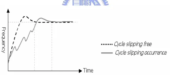
The second issue is the effect of cycle slipping phenomenon [29-31]. The cycle slipping in PLL is a statistical nonlinear phenomenon. It occurs when a large frequency error is presented to the phase detector and the loop bandwidth is not sufficient to correct for it in a fast time frame. The phase detector then causes a temporary correction in the opposite direction than it should. The result of this phenomenon is extra time required for the phase detector to lock to the correct frequency. The net impact of cycle slipping is that it increases lock time as shown in Fig. 2.15. The cycle slipping occurs generally in situations where the comparison frequency is very high relative to the loop bandwidth. In general, if the comparison frequency exceeds about 100 times the loop bandwidth, cycle slipping begins to emerge as a problem.
Fig. 2.15. The impact of cycle slipping on lock time
The cycle slipping phenomenon can be explored from the characteristics of a conventional three-state phase detector. The three-state phase detector (PD) was firstly reported in reference [32], it is also a phase/frequency detector (PFD). The conventional three-state phase detector architecture is illustrated in Fig. 2.16(a). It consists of two D-flip-flops (DFF) and a NAND gate. The NAND gate is employed to provide a self-reset path. The state diagram is shown in Fig. 2.16(b). Initially, the
phase detector is in Init state and both UP and DN signals are low. When one of the PFD inputs rises, the corresponding output becomes high. The state of the finite-state machine (FSM) moves from an initial Init state to an Up or Down state. The state is held until the second input goes high, which in turn resets the circuit and returns the FSM to the initial state.
Fig. 2.16. (a) Conventional three-state phase detector architecture (b) State diagram of the three-state phase detector
The characteristic of PFD is ideally linear for the entire range of input phase difference from 2π to -2π as shown in Fig. 2.17(a). However, due to the finite delay of the reset path, the linear range is less than 4π. This nonideal linear PFD characteristic is shown in Fig. 2.17(b). There are gain inversion regions near ±2π. The effect appears as a negative output for phase difference approaching ±2π. The width of the gain inversion region depends on the reset path delay, which is determined by the propagation delay of logic gates. The PFD nonideal behavior due to nonzero reset path delay is shown in Fig. 2.18. The CLK_ref leads the CLK_div that activates an UP signal. As the input phase difference approaches 2π, the next leading edge CLK_ref arrives before the DFFs are reset due to the nonzero reset path delay. The reset signal RB overrides the new CLK_ref edge and does not activate the UP signal. The subsequent CLK_div edge activates a DN signal, but it is wrong information. During acquisition, the frequency will not monotonically approach
lock-in range because the nonideal PFD gives the wrong information periodically. The acquisition process slows by how often the wrong information occurs. If the reset path delay equalsπ, i.e. in high frequency operation, the PFD outputs the wrong information half the time and, thus, fails to acquire frequency lock unconditionally.
In this design, a 2-cycle frequency search method cooperating with a new PFD structure can prevent the cycle slipping occurrence.
Fig. 2.17. (a) Ideal linear PFD characteristic (b) Nonideal linear PFD characteristic
2.3.3 The Impact of Hsync Jitter Injection
Another design issue is the impact of Hsync jitter injection. The PLL reference clock source in the video display system is very different form the other electronic systems. Unlike most PLL reference clock coming from a precise oscillator, the Hsync signal is a mediocre quality clock source in the video display system. The following is the clock jitter measurement data of three commercial graphic cards [25]. The jitter may range from several hundred pico-seconds to more than one nano-second. The injection of such a large jitter into the PLL will cause the stability problem. The output jitter may cause spatial instability in the displayed image. Furthermore, an overmuch Hsync jitter will probably make the PLL unable to be locked. This malfunction will cause the image to be distorted seriously.
Besides these previously described design issues, the low refresh rate induced jitter, nonzero PFD dead zone, DCO resolution limitation, and working temperature variation are also important considerations of the PLL clock generator for video application circuit design.
Chapter 3
ADPLL Clock Generator Circuit
Design
3.1 The Proposed ADPLL Architecture
The proposed cell-based ADPLL clock generator architecture is shown in Fig. 3.1. The ADPLL consists of phase/frequency detector (PFD), control unit (CTRL), digital-controlled oscillator (DCO), phase adjustment circuit (ADJ), and clock counter (DCO_CNT). An RSTB control signal enables the ADPLL circuit. The MULTI signals are used for programming the clock divider. The input reference clock is CLK_IN, which comes from Hsync. The output clock CLK_DCOO and CLK_DIVO are generated high frequency pixel clock and low frequency divided clock respectively.
The digital control unit is the core of this ADPLL clock generator. It issues commands to control all the other functional blocks. The proposed PFD is a modified three-state phase/frequency detector without self-reset path. It compares the phase relation between the input reference clock and the feedback divided clock, and then sends the comparison results, IS_UP and IS_DN, back to the control unit. The control unit will speed up or slow down the DCO according to the comparison results. The proposed DCO circuit is a four-tuning-stage ring oscillator with enable part. The frequency of DCO is decided by the digital control words TUNE1, TUNE2, TUNE3, and TUNE4 from the control unit. The phase adjustment circuit is a fine delay line to deskew channel delay according to the external phase selection signal, ADJUST. The clock counter acts as a frequency divider. It receives the DCO clock and feeds back a
multiplication factor, MULTI. The details of these functional blocks will be presented in the next sections. The simulation waveform of the proposed ADPLL system is shown in Fig. 3.2.
Fig. 3.1. The proposed ADPLL clock generator architecture
3.2 Phase/Frequency Detector
The proposed PFD is a modified three-state PFD without self-reset path as shown in Fig. 3.3. When feedback divided clock CLK_DIV lags input reference clock CLK_IN, the UP signal goes to logic high and DN remains low. Then, the control signal PD_GET goes high to latch the comparison results. Thus the IS_UP state is asserted. Oppositely, when CLK_DIV leads CLK_IN, the IS_DN state is asserted. Afterward the control signal PD_RB goes low to reset the PFD and then goes high to prepare for receiving the arrival of input signals next time. The timing diagram of the proposed PFD is shown in Fig. 3.4. The generation of the control signals will be presented in section 3.5. By the way, the only information sent to the control unit is the phase difference polarity not magnitude.
Fig. 3.3. The schematic of the proposed PFD
An important performance index of PFD is dead-zone. The so-called dead-zone is a very small region of PFD characteristics where the phase difference is around 0. The PFD cannot detect the phase relation of input reference and feedback divided clocks correctly within this region. In other words, the PFD is unable to generate correct information when the two input clock phases are very close. The cause of dead-zone comes from the response time of the devices. The dead-zone usually ranges from several to several tens pico-seconds. There have been plenty studies of PFD dead-zone problem published [33-48]. Most of them use dynamic logic techniques to improve the dead-zone. However, it cannot apply to a low refresh rate ADPLL.
The simulation result of the proposed PFD is shown in Fig. 3.5. The phase difference between CLK_IN and CLK_DIV is 1ps. The PFD can output correct information in different simulation conditions. The dead-zone of the proposed PFD is 1ps according to this simulation result.
Fig. 3.5. The simulation result of the proposed PFD
Note: The divided clock lags reference clock by 1ps. The PFD can latch correct information in different simulation conditions: (A)TT/1.0V/40°C (B)SS/0.9V/120°C (C)FF/1.1V/-40°C (D)FNSP/1.0V/40°C (E)SNFP/1.0V/40°C
3.3 Digital-Controlled Oscillator
The proposed DCO is a four-tuning-stage ring oscillator with enable part as shown in Fig. 3.6. The four stages are: (1)successive approximation register (SAR), (2)linear (LIN), (3)first DCO dithering (DIT1), and (4)second DCO dithering (DIT2). The first three stages are utilized as frequency searching, and the last stage is utilized as phase tracking. These tuning stages are governed by the control unit. The control flow chart will be presented in section 3.5.
Fig. 3.6. The schematic of the proposed DCO
The most basic requirement of the DCO circuit is the delay line range, that is, the DCO operation frequency range has to cover all the display modes. In order to meet all the display modes from VGA to UXGA, the DCO frequency range must cover 25MHz (40ns) to 230MHz (4.34ns) under different operation conditions. Hence the DCO tuning range must be more than 35.66ns (40ns-4.34ns=35.66ns). The proposed DCO frequency range is dominated by the tuning range of the first SAR stage. The schematic of the proposed SAR tuning stage is shown in Fig. 3.7. This stage is used to achieve fast frequency search. It is composed of 12 cascaded binary-weighted delay paths controlled by TUNE1[11:0]. Each delay cell consists of a multiplexer and a different weighted delay path. The control signal decides which path to be selected, thus one of 4096 delay path combinations could be chosen
through the 12-bit control word. The simulation result of each SAR stage tuning range corresponding to the control code TUNE1[11:0] is shown in table. 3.1. The minimum tuning range in fast case is 40.118 ns. It can be seen that the proposed DCO can apply to the all the display modes.
Fig. 3.7. The schematic of the proposed SAR tuning stage
Table. 3.1. The tuning range simulation result of the SAR stage
The linear tuning stage is shown in Fig. 3.9. The purpose of this linear stage is to acquire a more accurate frequency after SAR stage. It consists of 8 delay cells, and
each cell is composed of a buffer and two digitally controlled varactors (DCV) [49,50]. The DCV array is controlled by the 16-bit thermometer code which decoded from TUNE2[3:0]. The simulation result of this linear stage delay time corresponding to the control word is listed in table 3.2. It can be seen that the DCV cell can achieve 6ps high resolution in worst case.
Fig. 3.8. The schematic of the proposed linear tuning stage
Next, the DCO dithering stages are employed to minimize the frequency error and tracking error. Each stage is controlled by one single bit to alter the delay time. The control mechanism will be presented in section 3.5. The tuning range simulation results of the DCO dithering stages is listed in table 3.3. The tuning resolutions of the third and fourth stages are 168ps and 17ps respectively in worst case according to the simulation result. Because there is tradeoff between DCO resolution and tracking ability, a very small tuning step of the fourth stage is not necessary.
Fig. 3.9. The schematic of the proposed DCO dithering stages
Table. 3.3. The tuning range simulation result of the DCO dithering stages In short, the simulation result of the overall DCO operation range is shown in table 3.4. The maximum DCO frequency is 237MHz (4212ps) in slow case, and the minimum DCO frequency is 23.8MHz (41848ps) in fast case. Thus, the DCO can fully support all the display modes from VGA to UXGA.
3.4 Phase Adjustment Circuit
The purpose of the phase adjustment circuit is to deskew channel delay such that the sampling clock can be fine tuned to the best timing. It is a 16-step adjustable delay line controlled by ADJUST[3:0]. It is composed of 16 delay stages and a thermometer decoder, and each delay stage consists of a NAND and MUX to decide which path to be chosen [51,52]. The adjustment step is 410ps in slow case according to the simulation result listed in table 3.5.
Fig. 3.10. The schematic of the proposed phase adjustment circuit
3.5 Control Unit
The control unit is the core of the ADPLL clock generator. It receives the comparison result of PFD and modifies the DCO control code until the loop is locked. The detail state and timing diagrams will be presented in this section.
3.5.1 State Diagram of Control Unit
The state diagram of the control unit is shown in Fig. 3.11. The control algorithm will influence the frequency lock time and tracking performance of the loop.
Fig. 3.11. The state diagram of control unit
The first state is successive approximation register (SAR) tuning stage. The default values of the SAR control bits are all zeroes except the first bit, i.e. TUNE1[11:0]=12’b1000_0000_0000 (refer to Fig. 3.7.). The control code is scanned bit by bit from the most significant bit (MSB) to the least significant bit (LSB). A counter is employed to record the current SAR step. If the PFD returns IS_UP, the
control unit resets the current SAR control bit to logic 0 and sets next bit to logic 1 in order to speed up DCO frequency. In another situation, if the PFD returns IS_DN, the control unit keeps the current SAR control bit as logic 1 and sets the next bit to logic 1 in order to slow down the DCO frequency. By means of the SAR algorithm and binary-weighted DCO design, the fast frequency search can be achieved owing to the variable loop bandwidth. The loop bandwidth is quite high in the beginning and relatively small in the end of SAR state. The frequency search time depends on how many bits is the SAR control code. For instance, it takes n steps for an n-bits SAR control code. It takes 12 steps to finish the SAR frequency search process in the proposed chip.
The second state is linear (LIN) tuning stage. The purpose of this stage is to acquire a more accurate frequency after SAR stage. Thus the tuning resolution must be much higher than the first stage. The default values of the LIN control bits are half zeroes and half ones through a thermometer decoder, that is TUNE2[3:0]=4’b1000 while C[15:0]=16’b0000_0000_1111_1111 (refer to Fig. 3.8.). If the PFD returns IS_UP, the control unit decreases the LIN control code, which asserts less ones, to speed up the DCO frequency, and vice versa. The frequency search time is proportional to the width of control code. It equals 2n-1 steps for an n-bits LIN control code. As a result, it takes 8 steps to complete the LIN frequency search process in the proposed chip.
The third state is DCO dithering (DIT1) tuning stage. The control unit enters this stage as the PFD comparison result is changed. This means that the DCO frequency is quite close to the target frequency. This stage is intended to minimize the frequency error after the first two stages. Sometimes it is not possible to find a control code that exactly fulfils the multiple relations between input and output clock owing to the DCO resolution limitation. Therefore, the fraction-N PLL architecture is
introduced to enhance the tuning resolution and flexibility [55,56]. However, the multiple relations between input and output clocks are not fixed in different cycles. The fractional-N architecture is not feasible in the video application. Another solution to enhance the tuning resolution is the DCO dithering method [54]. The concept of DCO dithering is to alter the output clock period during one reference cycle and keep the multiple relation as shown in Fig.3.12. The period of CLK_DCO is controlled by TUNE signal. When TUNE is logic 1, the CLK_DCO is dithering to long period by increasing Δt whereΔt is the original DCO tuning resolution. From this figure, the DCO clock frequency keeps 10 times of the reference clock, and the period of the DCO clock is T0+Δt/2 on average. It can be seen that the DCO resolution is thus
doubled without an extremely high resolution DCO. The resolution enhancement level is determined by the frequency multiplication factor and how many cycles are dithered during one reference cycle. In the proposed design, a fractional and a step counters with binary search algorithm are exploited to decide how many DCO clock must be dithered. The frequency search time of this DCO dithering stage is determined by the width of the step counter. This stage ends up when the dithering step counter equals zero. For a n-bits counter, the binary search process takes n*2 steps. In the proposed design, the step counter is 10-bits, thus takes at most 20 steps to complete the frequency search process. As this DCO dithering stage finishes the frequency error is minimized and the PLL is locked to the desired frequency.
The final state is another DCO dithering (DIT2) stage. The behavior of this stage is similar to the first dithering stage. The PLL starts phase tracking when enters this stage. When the PFD returns IS_DN, more clocks are dithering as long period in order to realign with the reference clock. On the contrary, when the PFD returns IS_UP, fewer clocks are dithering as long period to catch up the reference clock.
3.5.2 Timing Diagram of Control Unit
The timing diagram of control unit is shown in Fig. 3.13. The state machine is in IDEL state during reset. When the reset signal RSTB releases and input reference clock activates, the state machine enters SAR, LIN, and DIT1 frequency search state sequentially. The frequency search states take 40 steps (12+8+20=40) to lock in the desired frequency. Because each frequency search step takes two reference cycles (this 2-cycle frequency compare method will be described thereafter), the frequency search process need totally 80 reference cycles to be finished. The PLL enters DIT2 phase tracking stage and the output signals CLK_DCOO and CLK_DIVO are activated once the frequency is locked. The detailed timing diagram of each state will be presented in the following.
The timing diagram of SAR frequency search state is shown in Fig. 3.14. When the first rising edge of reference clock CLK_ref comes, the DCO clock CLK_DCO is activated and the DCO counter dco_cnt starts up counting at timing (A). The dco_cnt keeps up counting until it equals M and then reset to 1 where M stands for the multiplication factor. The CLK_DIV goes high when dco_cnt equals 1 and goes low when dco_cnt equals M/8. Therefore, the duty cycle of divided clock CLK_DIV is 12.5% which is similar to Hsync. A sequence of commands is generated by CLK_DCO after each CLK_ref depending on the state machine. Here, PFD_EN command is activated to enable PFD at timing (B). After that, the second rising edge of CLK_ref arrives and another sequence of commands is generated. This time, a PFD_GET command is issued to latch the PFD comparison result at timing (C), and then a PFD_DIS command is issued to reset the PFD at timing (D) because the PFD has no self-reset path. In this example, a IS_UP information is latched because the divided clock CLK_DIV lags the reference clock CLK_ref. Next, a DCO_DIS command is activated to disable DCO thus stops DCO clock, and a DCO_TUNE command is activated to modify the DCO control code at timing (E). In this example, the divided clock lags the reference clock. The fifth bit of DCO control code TUNE1 is set to logic 0 and the fourth bit is set logic 1 in order to speed up DCO. Finally, the next rising edge of CLK_ref comes and starts another frequency search step at timing (F). This is the operation of 2-cycle frequency compare method.
It is worthy of noticing that this 2-cycle frequency compare method benefits in two important points. First, there is no accumulation error during frequency search process because DCO clock realigns with reference clock at the beginning of each search step. Consequently, the loop can acquire the target frequency correctly without the disturbance of the accumulation error. Second, the cycle slipping phenomenon is eluded in co-ordination with the proposed PFD because the PFD never operates in the
gain inversion region. Therefore, the loop can lock to the target frequency quickly.
Fig. 3.14. The timing diagram of SAR frequency search state
Note: (A) Start frequency search and enable DCO at first reference clock (B) Enable PFD
(C) Latch PFD comparison result (D) Reset PFD
(E) Disable DCO and tune DCO SAR control code (F) Start next frequency search step and enable DCO
The timing diagram of LIN frequency search state is shown in Fig. 3.15. The 2-cycle frequency compare operation is similar to SAR stage except that an extra PFD_JUDGE command is activated after the second rising edge of CLK_ref to detect whether the PFD polarity changes, either from IS_UP to IS_DN or from IS_DN to IS_UP, at timing (C). If the PFD polarity changes, a PFD_CHANGE signal is asserted to denote the end of LIN stage. In this example, the divided clock leads the reference clock. The control code TUNE2 is modified from 4’b1000 to 4’b1001 to slow down the DCO clock.
Fig. 3.15. The timing diagram of LIN frequency search state
Note: (A) Start frequency search and enable DCO at first reference clock (B) Enable PFD
(C) Detect PFD status transition (D) Latch PFD comparison result (E) Reset PFD
(F) Disable DCO and tune DCO LIN control code (G) Start next frequency search step and enable DCO
The timing diagram of DIT1 frequency search state is shown in Fig. 3.16. The operation is a little different from the previous stages. There are two counters used to calculate how many DCO clocks to be dithered in order to minimize the frequency error. One is the fractional counter fra_cnt3 which records how many clocks to be dithered, and its default value is M/2. The DCO dithering control signal is low when DCO counter reset to 1, and the control signal goes high while DCO counter equals fractional counter. The DCO clock is dithering to long period when control signal is high. As a result, more clocks are dithered as long period cycles when the fractional
counter is smaller, and vice versa. Another is the step counter fra_step3 which records tuning step, and its default value is M/4. The step counter is divided by 2 if the PFD_JUDGE command detects the PFD polarity change at timing (C). Then the fractional counter updates its content by adding or subtracting the step counter value according to the PFD comparison result at timing (F). This binary search process continues till the step counter equals zero. According to Fig. 3.16, the step counter is divided by 2 (250/2=125) because the PFD polarity changes. Because the divided clock leads reference clock, the fraction counter updates its content by subtracting from the value of step counter to increase the number of dithering long cycles so that the period of divided clock can be extended to realign with reference clock again.
Fig. 3.16. The timing diagram of DIT1 frequency search state
Note: (A) Start frequency search and enable DCO at first reference clock (B) Enable PFD
(C) Detect PFD status transition (D) Latch PFD comparison result (E) Reset PFD
(F) Disable DCO and tune DCO DIT1 control code (G) Start next frequency search step and enable DCO
After the previous three frequency search stages, the chip enters phase tracking stage. The timing diagram of DIT2 phase tracking state is shown in Fig. 3.17. The operation principle is similar to that of DIT1 stage. The major difference is that the DCO is not disabled and the PFD is enabled at timing (D). If the PFD polarity changes at timing (A), the fractional counter will be restored to the default value, M/2, at timing (D). In addition, the step counter is a configurable value.
Fig. 3.17. The timing diagram of DIT2 phase tracking state
Note: (A) Detect PFD status transition (B) Latch PFD comparison result (C) Reset PFD
Chapter 4
Chip Implementation
4.1 Chip Layout
The ADPLL core circuit layout is shown in Fig. 4.1. This chip is fabricated by UMC 90nm 1P9M logic/mixed-mode standard CMOS process. The total gate count is 2.4K, and the chip size is 100x100um2.
Fig. 4.1. The ADPLL core circuit layout
4.2 Circuit Simulation Result
The simulation result of the proposed DCO is shown in table 4.1. It can be seen that the proposed DCO can cover 4375ps to 39721ps operation range in all simulation conditions. The proposed adjustment circuit simulation result is shown in table 4.2.
Table 4.1. The proposed DCO simulation result
Table 4.2. The proposed adjustment circuit simulation result
It is not efficient to simulate the full chip performance in the conventional analog simulation environment because of the low refresh rate input clock. It may take more than one month to finish a simulation run time. In order to speed up the simulation and keep acceptable accuracy, a mixed-mode simulation environment as shown in Fig. 4.2 is built up to achieve this goal. Only the critical analog parts, DCO, PFD, and ADL, is in simulated in analog level. The full chip simulation result of the proposed ADPLL is shown in table 4.3. The simulation condition is TT/1.0v/40°c with ±200ps input clock jitter for 500 cycles.
Fig. 4.2. Mixed-mode simulation environment
Table 4.3. The proposed ADPLL full chip simulation result
4.3 Chip Measurement Result
The ADPLL functional test waveform is shown in Fig.4.3. The input clock is 100KHz, and the multiplication factor is 2000. The output clock is 200MHz and the lock time is 70 reference clock cycles. From this waveform, we can see that the internal DCO clock, CLK_DCOX, is on and off during frequency search stages.
The output pixel clock measurement result is shown in Fig.4.4. There are two peaks in the period histogram because of the dithering method. The test condition is SXGA mode (M=1688, Input=64.5KHz, Output=108.9MHz). The phase difference between input reference clock and output divided clock measure result is shown in Fig.4.5.
Fig. 4.4 Pixel clock measurement result
Finally, the chip measurement summary is listed in table 4.4. The input jitter is more than 1ns. The power consumption is 3mW in UXGA mode.
Table 4.4. The ADPLL test chip measurement summary
There are differences between simulation and measurement results. The full chip simulation result shows that the chip performance meets the design specification, however the measurement result is quite different from the simulation result. The main issue is the Hsync jitter injection and noise of the test environment. A behavior model simulation of the proposed ADPLL with different input jitter is shown in Fig. 4.6. From this simulation result, it can be seen that the input jitter affects the phase drift performance directly so the quality of clock source will influence the loop performance significantly.
Chapter 5
Conclusion and Future Work
In this thesis, we proposed a large frequency multiplication factor, low power, cell-based ADPLL clock generator for video application. The all-digital cell-based design is portable for different manufacture processes without too much redesign effort. A 4-stage DCO with 18-bit control word is constructed to cover the wide operating range from 25MHz to 230MHz. The SAR and binary frequency search method can achieve fast lock-in time that less than 80 reference cycles. A 2-cycle frequency comparison method can prevent cycle slipping phenomenon and obtain accurate frequency without suffering the phase error accumulation. A new PFD structure with 1ps dead zone is also employed to provide accurate phase comparison information. In order to improve the phase tracking ability and keep low output jitter without extremely high resolution oscillator, the DCO dithering method is introduced to achieve this goal. Finally, the chip is implemented by UMC 90nm 1P9M logic/mixed-mode standard CMOS process. The total gate count is 2.4K, and the chip size is 100x100um2.
Though the chip measurement result is quite different from the circuit simulation result, the best measurement result in SXGA still gets 6.9ns phase difference (75% of pixel clock period). This might be resulted from the Hsync jitter injection, the noise of testing environment, inadequate power bus route, or imperfect layout partition.
The most important topics for further improving the ADPLL performance are how to minimize the impact of Hsync jitter injection and how to enhance the tracking performance by different DCO dithering method.
Reference
[1] Dao-Long Chen, “Designing On-Chip Clock Generators,” IEEE Circuits and
Devices Magazine, Vol. 8, Issue 4, Jul. 1992, pp.32-36
[2] Vincent R. von Kaenel, “A High-Speed, Low-Power Clock Generator for a Microprocessor Application,” IEEE Journal of Solid-State Circuit (JSSC), Vol.
33, Issue 11, Nov. 1998, pp.1634-1639
[3] Young I.A., Greason J.K., Wong K.L., “A PLL Clock Generator with 5 to 110 MHz of Lock Range for Microprocessors,” IEEE Journal of Solid-State Circuit
(JSSC), Vol. 27, Issue 11, Nov. 1992, pp.1599-1607
[4] Vincent von Kaenel, Daniel Aebischer, Christian Piguet, Evert Dijkstra, “A 320 MHz, 1.5 mW @ 1.35 V CMOS PLL for Microprocessor Clock Generation,”
IEEE Journal of Solid-State Circuit (JSSC), Vol. 31, Issue 11, Nov. 1996, pp.1715-1722
[5] David W. Boerstler, “A Low-Jitter PLL Clock Generator for Microprocessors with Lock Range of 340-612 MHz,” IEEE Journal of Solid-State Circuit (JSSC),
Vol. 34, Issue 4, Apr. 1999, pp.513-519
[6] Hyung-Rok Lee, Ook Kim, Gijung Ahn, Deog-Kyoon Jeong, “A Low-Jitter 5000ppm Spread Spectrum Clock Generator for Multi-channel SATA Transceiver in 0.18um CMOS,” IEEE International Solid-State Circuits
Conference (ISSCC), Vol. 1, Feb. 2005, pp.162-163
[7] Lizhong Sun, Kwasniewski T., “A 1.25GHz 0.35um Monolithic CMOS PLL Clock Generator for Data Communications,” IEEE Custom Integrated Circuits
Preceedings, May 1999, pp.265-268
[8] Jeong D.K., Borriello G., Hodges D.A., Katz R.H., “Design of PLL-Based Clock Generation Circuits,” IEEE Journal of Solid-State Circuit (JSSC), Vol. 22, Issue 2,
Apr. 1987, pp.255-261
[9] Jim Dunning, Gerald Garcia, Jim Lundberg, Ed Nuckolls, “An All-Digital Phase-Locked Loop with 50-Cycle Lock Time Suitable for High-Performance Microprocessor,” IEEE Journal of Solid-State Circuit (JSSC), Vol. 30, NO. 4, Apr.
1995, pp.412-422
[10] Kuo-Hsing Cheng, Yu-Jung Chen, “A Novel All Digital Phase Locked Loop with Ultra Fas t Locked Time and High Oscillation Frequency,” IEEE International
ASIC/SOC Conference , Sep. 2001, pp.139-143
[11] Thomas Olsson, Peter Nilsson, “A Digitally Controlled PLL for SoC
Application,” IEEE Journal of Solid-State Circuit (JSSC), Vol. 39, Issue 5, May
[12] Michel Combes, Karim Dioury, Alain Greiner, “A Portable Clock Multiplier Generator Using Digital CMOS Standard Cells,” IEEE Journal of Solid-State
Circuit (JSSC), Vol. 31, Issue 7, Jul. 1996, pp.958-965
[13] Ching-Che Chung, Chen-Yi Lee, “An All-Digital Phase-Locked Loop for
High-Speed Clock Generation,” IEEE Journal of Solid-State Circuit (JSSC), Vol.
38, NO. 2, Feb. 2003, pp.347-351
[14] Marie H., Belin P., “R, G, B Acquisition Interface with Line Locked Clock Generator for Flat Panel Display,” IEEE Journal of Solid-State Circuit (JSSC),
Vol. 33, Issue 7, Jul. 1998, pp.1009-1013
[15] Begueret J., Deval Y., Mazouffre O., Spataro A., Fouillat P., Benoit E., Mendoza J., “Clock Generator Using Factorial DLL for Video Applications,” IEEE
Conference on Custom Integrated Circuits, May. 2001, pp.485-488
[16] Terukina A., Nozawa T., Suzuki Y., Hino A., Koyama S., Moritani A., “A High Precision CMOS Clock Generator for Optimum Sampling of Analog RGB Data,” IEEE Conference on Custom Integrated Circuits, May. 1993, pp.
27.3.1-27.3.4
[17] Suzuki Y., Gai T., Yamakawa M., Sugiura H., Moritani A., “NTSC/PAL/SECAM Digital Video Decoder with High-Precision Resamplers,” IEEE Transactions on
Consumer Electronics, Vol. 51, Issue 1, Feb. 2005, pp. 287-294
[18] Sandeep Agarwal, Arun Johary, “PIXEL CLOCK PLL FREQUENCY AND PHASE OPTIMIZATION IN SAMPLING OF VIDEO SIGNALS FOR HIGH QUALITY IMAGE DISPLAY,” U.S. patent 6933937 B2, Aug. 23 2005
[19] Gretchen T. Gaskill, Robert J. Vitello, “PLL-BASED METHOD AND APPARATUS FOR GENERATING VIDEO DRIVE SIGNALS FROM VARIOUS SYNC FORMATS,” U.S. patent 5502502, Mar. 26 1996
[20] Paul von Hase, “Method and device to adjust the phase in a flat-screen,” R.O.C.
patent 89105471, Mar. 28 2002
[21] Cyrus Chu, Wen-Yi Huang, “METHOD FOR REDUCING ANALOG PLL JITTER IN VIDEO APPLICATION,” R.O.C. patent 94129265, Aug. 26 2005 [22] Rodda W.E., Campbell E.R., Sauer D.J., Mayweather W.T., Dell'ova F., “Full
CMOS Video Line-Locked Phase-Locked Loop System,” IEEE Transactions on
Consumer Electronics, Vol. 39, No. 3, Aug. 1993, pp.496-503
[23] “Video Capture PLL,” Analog Bits Inc. Datasheet
[24] “Low Refresh Rate PLL IP Core targeted at Video and Flat Panel Display Applications,” CEVA Inc. Datasheet
[26] Rafael Fried, Ziv Azmanov, “Low Power Digital PLL with One Cycle Frequency Lock-in Time and Large Frequency Multiplication Factor for Advanced Power Management,” IEEE International Conference on Electronics, Circuits, and
Systems (ICECS), Vol. 2 , Oct. 1996, pp.1166-1169
[27] Takamoto Watanabe, Shigenori Yamauchi, “An All-Digital PLL for Frequency Multiplication by 4 to 1022 with Seven-Cycle Lock Time,” IEEE Journal of
Solid-State Circuit (JSSC), Vol. 38, NO. 2, Feb. 2003, pp.198-204
[28] Maneatis J.G., Kim J., McClatchie I., Maxey J., Shankaradas M., “Self-Biased High-Bandwidth Low-Jitter 1-to-4096 Multiplier Clock Generator PLL,” IEEE
Journal of Solid-State Circuit (JSSC), Vol. 38, Issue 11, Nov. 2003, pp.1795-1803
[29] Mozhgan Mansuri, Dean Liu, Chih-Kong Ken Yang, “Fast Frequency
Acquisition Phase-Frequency Detectors for Gsamples/s Phase-Locked Loops,”
IEEE Journal of Solid-State Circuit (JSSC), Vol. 37, NO. 10, Oct. 2002, pp.1331-1334
[30] Kun-Seok Lee, Byeong-Ha Park, Han-il Lee, Min Jong Yoh, “Phase frequency detectors for fast frequency acquisition in zero-dead-zone CPPLLs for mobile communication systems,” IEEE European Solid-State Circuits Conference
(ESSCIRC), Sep. 2003, pp.525-528
[31] Dean Banerjee, Paul Boyer, “Delta Sigma PLLs Raise The Standard For Performance,” National Semiconductor Application Brief 125, 2003 [32] C. Andrew Sharpe, “A 3-state phase detector can improve your next PLL
design,” EDN magazine, Sep. 1976, pp.224-228
[33] Rami Ahola, Saska Lindfors, Jarkko Routama, Kari Halonen , “A Novel Phase Detector with No Dead Zone and a Chargepump with Very Wide Output Voltage Range,” IEEE European Solid-State Circuits Conference (ESSCIRC), Sep.1998,
pp.352-355
[34] Sang-O Jeon, Tae-Sik Cheung, Woo-Young Choi, “Phase/frequency detectors for high-speed PLL applications,” IEE Electronics Letters, Vol. 34, No.22, Oct. 1998,
pp. 2120-2121
[35] Lee G.B., Chan P.K., Siek L., “A CMOS Phase Frequency Detector for Charge Pump Phase-Locked Loop,” Midwest Symposium on Circuits and Systems, Vol. 2,
Aug. 1999, pp.601-604
[36] Johansson H.O., “A Simple Precharged CMOS Phase Frequency Detector,”
IEEE Journal of Solid-State Circuit (JSSC), Vol. 33, NO. 2, Feb. 1998, pp.295-299
[37] Chien-Ping Chou, Zhi-Ming Lin, Jun-Da Chen, “A 3-ps dead-zone double-edge-checking phase-frequency-detector with 4.78 GHz operating frequencies,” Proceedings of IEEE Asia-Pacific Conference on Circuits and
[38] Rui-feng Liu, Yong-ming Li, Hong-yi Chen, “A fully symmetrical PFD for fast locking low jitter PLL,” Proceedings of Internal Conference on ASIC, Vol. 2, Oct.
2003, pp.725-727
[39] Kuo-Hsing Cheng, Tse-Hua Yao, Shu-Yu Jiang, Wei-Bin Yang, “A Difference Detector PFD for Low Jitter PLL,” IEEE International Conference on Electronics, Circuits, and Systems (ICECS), Vol. 1 , Sep. 2001, pp.43-46
[40] Chang, R.C., Lung-Chih Kuo, “A differential type CMOS phase frequency detector,”
Proceedings of IEEE Asia Pacific Conference on ASIC(AP-ASIC), Aug. 2000, pp.61-64
[41] Harufusa Kondoh, Hiromi Notani, Tsutomu Yoshimura, Hiroshi Shibata, Yoshio Matsuda, “A 1.5V 250MHz to 3.0V 622NHz Operation CMOS Phase-Locked Loop with Precharge Type Phase-Frequency Detector,” IEICE transactions on
electronics, Vol. E78-C, No. 4, Apr. 1995, pp.381-388
[42] Hwang-Cherng Chow, Yeh N.-L., “A New Phase-Locked Loop with High Speed Phase Frequency Detector,” Midwest Symposium on Circuits and Systems, Vol. 2,
Aug. 2005, pp.1342-1345
[43] Hyuk-Jun Sung, Kwang Sub Yoon, Hong Ki Min, “A 3.3 V high speed dual looped CMOS PLL with wide input locking range,” Midwest Symposium on
Circuits and Systems, Aug. 1998, pp.476-4792
[44] Won-Hyo Lee, Jun-Dong Cho, Sung-Dae Lee, “A High Speed and Low Power Phase-Frequency Detector and Charge-pump,” IEEE Asia and South Pacific
Design Automation Conference (ASP-DAC), Vol. 1, Jan. 1999, pp.269-27
[45] Gotoh K., Wakayama S., Saito M., Ogawa J., Tamura H., Okajima Y., Taguchi M., “All-digital Multi-phase Delay Locked Loop For Internal Timing Generation In Embedded And/or High-speed DRAMs,” Symposium on VLSI Circuit Digest
of Technical Papers, Jun. 1997, pp.107-108
[46] Christiansen, J., “An integrated high resolution CMOS timing generator based on an array of delay locked loops,” IEEE Journal of Solid-State Circuit (JSSC), Vol.
31, No. 7, Jul. 1996, pp.952-957
[47] Donald R. Preslar, “DIGITAL PHASE COMPARATOR WITH IMPROVED SENSITIVITY FOR SMALL PHASE DIFFERENCES,” U.S. patent 4322643,
Mar. 30, 1982
[48] John D. Hatchett, Andrew S. Olesin, “LINEARIZED DIGITAL PHASE AND FREQUENCY DETECTOR,” U.S. patent 4378509, Mar. 29, 1983
[49] Pao-Lung Chen, Ching-Che Chung, Chen-Yi Lee, “A Portable Digitally Controlled Oscillator Using Novel Varactors,” IEEE Transactions on Circuits
and Systems II (TCSII): Express Briefs, Vol. 52, No. 5, May 2005, pp.233-237
[50] Jin-Jer Jong, Chen-Yi Lee, “A Novel Structure for Portable Digitally Controlled Oscillator,” IEEE International Symposium on Circuits and Systems (ISCAS), Vol.
[51] Chia-Tsun Wu, Wei Wang, I-Chyn Wey, An-Yeu Wu, “A Scalable DCO Design for Portable ADPLL Designs,” IEEE International Symposium on Circuits and
Systems (ISCAS), Vol. 6, May 2005, pp. 5449-5452
[52] Roth E., Thalmann M., Felber N., Fichtner W., “A Delay-line Based DCO for Multimedia Applications Using Digital Standard Cells Only,” IEEE International
Solid-State Circuits Conference (ISSCC), Vol. 1, 2003, pp.432-505
[53] Shigenori Yamauchi, Takamoto Watanabe, Yoshinori Ohtsuka,, “RING
OSCILLATOR AND PULSE PHASE DIFFERENCE ENCODING CIRCUIT,”
U.S. patent 5146444, Jun. 18 1996
[54] Staszewski R.B., Chih-Ming Hung, Leipold D., Balsara P.T., “A First
Multigigahertz Digitally Controlled Oscillator for Wireless Applications,” IEEE
Transactions on Microwave Theory and Techniques, Vol. 51, Issue 11, Nov. 2003, pp. 2154-2164
[55] Ian Galton, “Delta-Sigma Fractional-N Phase-Locked Loops,” Phase-Locking in
High-Performance System, Behzad Razavi, IEEE press, 2003, pp.23-33
[56] Tom A.D. Riley, Miles A. Copeland, Ted A. Kwasniewski, “Dlta-Sigma
Modulation in Fractional-N Frequency Synthesis,” IEEE Journal of Solid-State
Circuits (JSSC), vol. 28, No. 5, May 1993, pp.553-559
[57] “Monitor Timing Specifications,” VESA and Industry Standards and Guidelines
Vita
Wen-Ming Huang was born in Taipei, Taiwan, in 1975. He
received the B.S. degree from National Cheng Kung University, Tainan, Taiwan, in 1997. He served as a design engineer in the video micro-controller department of Myson Technology Inc. in October 2000. Since August 2004, he joined the embedded flash memory team of UMC as a design engineer. His research interests include micro-controller system design, embedded memory circuit design, and SoC design methodology.
![Fig. 2.6. Video line-locked PLL block diagram [22]](https://thumb-ap.123doks.com/thumbv2/9libinfo/8470845.183534/19.892.149.724.786.1115/fig-video-line-locked-pll-block-diagram.webp)
![Fig. 2.7. Control mode flow chart [22]](https://thumb-ap.123doks.com/thumbv2/9libinfo/8470845.183534/20.892.145.723.571.1078/fig-control-mode-flow-chart.webp)
![Fig. 2.8. Video capture PLL [23]](https://thumb-ap.123doks.com/thumbv2/9libinfo/8470845.183534/21.892.145.725.487.895/fig-video-capture-pll.webp)
![Fig. 2.12. A 1 to 4096 multiplication factor PLL [28]](https://thumb-ap.123doks.com/thumbv2/9libinfo/8470845.183534/25.892.151.740.115.403/fig-a-to-multiplication-factor-pll.webp)