國 立 交 通 大 學
材料科學與工程學系
博 士 論 文
在金剛烷披覆之矽基材上探討鑽石的成核、成長
與結構特性之研究
The study of nucleation, growth, and structural
characterization of diamond on adamantane-
coated Si substrate
研 究 生 : Rajanish Nath Tiwari
指導教授 : 張 立 教授
在金剛烷披覆之矽基材上探討 鑽石的成核、成長
與結構特性之研究
The study of nucleation, growth, and structural
characterization of diamond on adamantane-
coated Si substrate
研 究 生: Rajanish Nath Tiwari
Student: Rajanish Nath Tiwari
指導教授: 張 立 博士
Advisor: Dr. Li Chang
國 立 交 通 大 學
材料科學與工程學系
博士論文
A Dissertation
Submitted to Department of Materials Science and Engineering
College of Engineering
National Chiao Tung University
in Partial Fulfillment of the Requirements
for the Degree of Doctor of Philosophy
in Materials Science and Engineering
November 2010
在金剛烷披覆之矽基材上探討 鑽石的成核、成長
與結構特性之研究
研究生:Rajanish Nath Tiwari
指導教授:張 立 博士
國立交通大學
材料科學與工程研究所
摘要
鑽石薄膜有許多優良的特性,特別是在電子、光電、和光學應用上有極大的 潛力。雖然鑽石合成技術已經達到了一個限度,在大面積商品化的需求下還存有一 些不明且難以解決的問題,特別是在較低的溫度與壓力下進行鑽石薄膜的合成。因 此,在本論文中,我們將會探討如何在較低的溫度(400~700°C)與壓力下進行鑽石 薄膜的製備。 我們使用微波電漿化學氣相沉積法(MPCVD)進行成長,通入氫氣與甲烷的混 合氣體作為反應用氣體,之後在披覆金剛烷(C10H16)的單晶矽基材上進行多晶鑽石 薄膜的合成,並與在未披覆金剛烷的矽基材上所成長的鑽石薄膜進行比較。 結果我們發現在披覆金剛烷的單晶矽基材上所成長的鑽石薄膜其成長速率比 未披覆金剛烷的快上兩倍。在單位面積中,其鑽石的分佈密度約為103 ~ 104 cm-2, 也比未披覆金剛烷的分佈密度高。在中間的成長階段,我們觀察到金剛烷先轉變為 與非晶碳相互混合的石墨相。隨後我們藉由X 光繞射 (XRD) 與 X 光光電子光譜儀 (XPS)進行鑽石薄膜的特性分析,證明了在鑽石沉積的過程中會形成碳化矽(SiC)界 面層。同時我們使用原子力顯微鏡(AFM)與拉曼光譜儀(Raman)能得知在矽基材上與高電流密度(1.6 mA/cm2)。另外,在矽基材(SiO2/Si)上使用鉑顆粒能夠吸附金剛 烷(碳氫化合物)並提升鑽石的成核密度高達 1012 ~ 1013 cm-2;並且,矽基材表面上 的氧化層能避免鉑和基材產生矽化反應,進而避免接下來鑽石的沉積過程中產生碳 化矽。在一開始沉積的兩分鐘內,金剛烷的晶種轉變成奈米鑽石和一些未分辨的碳 顆粒,並在之後 5 至 15 分鐘的沉積出現了石墨相。之後我們使用高倍率的掃描式 電子顯微鏡(SEM)發現以{111}、{100}和許多方向性的碳顆粒成為鑽石成長的成核 點。
The study of nucleation, growth, and structural
characterization of diamond on adamantane-
coated Si substrate
Student: Rajanish Nath Tiwari Advisor: Dr. Li Chang
Department of Materials Science and Engineering
National Chiao Tung University
Abstract
Diamond films have been regarded as an active field of science and technology because of their unique properties. Although the technology of diamond film was synthesized to an extent, some problems remain unclear and only their solution can result in wide-scale commercialization, especially as the synthesis of diamond film at low temperature and pressure. Therefore, in the thesis, we will discuss the synthesis of diamond film at relative low temperature (400 ~700°C) and pressure.
The polycrystalline crystalline diamond films were synthesized on adamantane (C10H16)-coated crystalline silicon substrates by microwave plasma chemical vapor deposition (MPCVD) from a gaseous mixture of methane and hydrogen gas without any mechanical and electrical pretreatments. Diamonds already grown on Si substrates without adamantane coating have been carried out as well as for comparison.
As a result, we observed that the growth rate of diamond film on adamantane-coated Si substrates were two times faster than without adamantane-coated. The density of diamond on adamantane coated were also ~103~4 cm-2 higher than that of without
adamantane coated. In the intermediate growth steps, we observed that the adamantane first converts into graphitic phase intermixed with amorphous carbon. The characterization of diamond films by x-ray diffraction (XRD) and x-ray photoelectron spectroscopy (XPS) show that the SiC interlayer have been formed during the diamond deposition. While atomic force microscope (AFM) and Raman spectra show the presence of nanodiamond phase on the Si substrate. The diamond films exhibit a low-threshold (55 V/μm) and high current density (1.6 mA/cm2) in their field-emission properties. In addition, using platinum particles on SiO2/Si substrates are adsorb adamantane (hydrocarbon) and increase the nucleation density ~1012~13 cm-2. The presence of oxide intermediate layer between Pt and Si prevents silicidation as well as SiC in diamond deposition. The seeded adamantane was first transformed into nanodiamond and some unidentified carbon particles in the early stage of deposition within 2 min while, further deposition (5-15 min) shows the existence of diamond and graphite phase. The high-magnification scanning electron microscope (SEM) have shown that the {111}, {100}, and many other orientated carbon particles may act as a nuclei for diamond growth.
Acknowledgements
I am indebted to many people who contributed in several ways to this work, and supported me with their cooperation and timely help.
In particular, I wish to express my sincere gratitude to my research supervisor Prof. Li Chang, for providing me an opportunity to work in his research group. I thank his for unique personal support in every aspect of the experimental work, for all the stimulating ideas, all the deep discussions, for providing support in preparation of various manuscripts for publications, presentations, posters and for the time he spent in reviewing this thesis. He has been a great mentor with his enthusiasm, understanding and willingness to help students professionally and personally.
I am extremely thankful to Mr. K. A. Chiu, Mrs. D. T. Hien, Mr. W.-L. Wang, Mr. W.-C. Chen, Mr. C.-S. Tian, and Mr. C.-Y. Peng, for serving my experimental supports and for their precious suggestions to my study. I would like to express my thanks to all my group members for their friendship: Dr. Y.-H. Wu, Mr. S. R. Sahoo, Mr. P.-H. Wu, and Ms. Y.-C. Chen. I am thankful to all my well-wishers particularly Mr. M. Hornansky and Dr. P.-Y. Kuo, who helped me directly and indirectly, and their emotional support, encouragement and inspiration were instrumental during all these years.
Most importantly, I wish to thank my entire extended family like to dedicate this work to my family particular my parents for their endless love and supports throughout my life. Their encouragement has been a source of inspiration that led to the completion of this thesis. I would like to thank everybody who was important to the successful realization of thesis, as well as expressing my apology that I could not mention personally one by one.
The financial support of my Ph.D. research work by a grant from the NCTU and NSC, Taiwan, R.O.C. is grateful acknowledged.
Contents
Abstract (in Chinese) --- I Abstract (in English) --- III Acknowledgements --- V Contents --- VI Abbreviations --- IX Table Captions --- XII Figure Captions --- XIII
Chapter 1 Introduction --- 1
1.1 Background --- 1
1.2 Motivation --- 2
Chapter 2 Literature Review --- 5
2.1 Graphite --- 5
2.2 Diamond --- 8
2.2.1 Natural production --- 10
2.2.2 Synthetic production --- 10
2.2.2.1 High Pressure and High Temperature Synthesis --- 11
2.2.2.2 Shock-wave Synthesis --- 13
2.2.2.3 Chemical Vapor Deposition --- 14
2.2.2.3.1 Hot Filament --- 15
2.2.2.3.2 Arcjet plasma --- 16
2.2.2.3.3 Microwave plasma --- 17
2.3 Properties and applications of diamond --- 19
2.4.2 Diamond growth mechanism --- 24
2.4.2.1 Gas phase Chemistry --- 25
2.4.2.2 Surface Chemistry --- 25
2.5 Diamonodoid Hydrocarbons --- 27
2.5.1 Lower diamondoids --- 28
2.5.2 Higher diamondoids --- 29
2.5.3 Properties and applications of lower diamondoids --- 31
2.6 Structure of Thesis --- 33
Chapter 3 Experimental methods --- 34
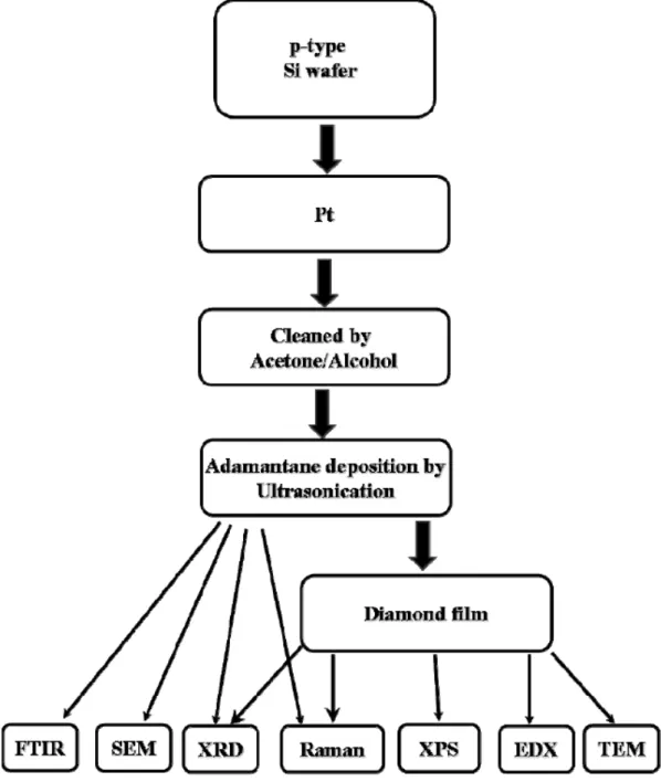
3.1 Experimental flowcharts --- 34
3.2 Substrate holder--- 37
3.3 MPCVD system --- 37
3.4 Material analysis methods --- 40
3.4.1 SEM --- 40
3.4.2 Micro Raman spectroscopy --- 41
3.4.3 TEM --- 42
3.4.4 XRD --- 44
3.4.5 XPS --- 45
3.4.6 AFM --- 46
3.5 Electron field emission measurements --- 48
Chapter 4 The Synthesis of diamond films on adamantane-coated Si substrate at low temperatures --- 49
4.1 Introduction --- 49
4.2 Experimental process for diamond synthesis --- 52 4.2.1 Coating of adamantane on Si substrates by hotplate method 52
4.3 Structural characterization of adamantane --- 55
4.4 Structural characterization of diamond at 200, 250, and 300W ---- 61
4.5 Hydrogen plasma on AC/Si substrates --- 68
4.6 Structural characterization of diamond at 350W --- 72
4.6.1 Diamond nucleation --- 72
4.6.2 Growth of continuous diamond film --- 80
4.7 Field emission measurement --- 89
4.8 Possible mechanisms for adamantane assisted diamond nucleation and growth Diamond nucleation--- 90
4.9 Summary --- 92
Chapter 5 Enhanced diamond nucleation on adamantane-coated Pt/Si substrates -- 93
5.1 Introduction --- 93
5.2 Experimental process for diamond growth --- 94
5.3 Structural characterization of adamantane --- 96
5.4 The early stage of deposition --- 98
5.5 Diamond formation after 120 min deposition time --- 109
5.6 Summary --- 117
Chapter 6 Conclusions and Future Works --- 118
6.1 Conclusions --- 118
6.2 Future Works--- 119
References --- 120
Appendix --- 134
Abbreviations
CVD Chemical vapor deposition
HTHP High temperature and high pressure
MCD Microcrystalline diamond
NCD Nanocrystalline diamond
UNCD Ultrananocrystalline diamond
MPCVD Microwave plasma chemical vapor deposition
BEN Bias enhanced nucleation
3D Three dimensions
HFCVD Hot filament chemical vapor deposition
MEMS Micro-electronic mechanical systems
G.C. Gas spectroscopy
SEM Scanning electron microscope
M.S. Mass spectrometry
SiC Silicon carbide
CH4 Methane C2H6 Ethane C2H2 acetylene C10H16 Adamantane C14H20 Diamantane C18H24 Triamantane AC Adamantane-coated Pt Platinum
TEM Transmission electron microscope
XRD X-ray diffraction
FTIR Fourier transform infrared spectroscopy
XPS X-ray photoelectron spectroscopy
OM Optical microscope
EFE Electron field emission
Ar Argon Mo Molybdenum
FIB Focused ion beam
D.F. Dark field
B.F. Bright field
EDX Energy-dispersive X-ray spectroscopy
FFT Fast Fourier transform
HRTEM High-resolution TEM
SAD Selected area diffraction
SAED Selected area electron diffraction
LTLP Low temperature and low pressure
N2 Nitrogen
SCCM Standard cubic centimeters per minute
WAC Without adamantane coated
nm nanometer
eV electron volt
BOE Buffer oxide etch
Al Aluminium cm centimeter
FCC face centered cubic
F-N Fowler-Nordheim mA milliampere
Table Captions
Table 2.1: Comparison of the bond strengths, crystal structure, transparency, thermal
conductivity, and electrical resistivity of diamond and graphite --- 6
Table 2.2: Diamond properties and its applications --- 2 0 Table 3.1: Raman characteristics of different carbon species of carbon --- 4 1 Table 4.1: Experimentally measured evaporation rate of adamantane at various
Figure Captions
Figure 2.1: Structure of (a) graphite and (b) diamond --- 6
Figure 2.2: Photographs of different kind of graphite --- 8
Figure 2.3: Theoretically predicted phase diagram of carbon --- 9
Figure 2.4: Carbon phase diagram with temperature and pressure ranges corresponding to various diamond synthesis process --- 12
Figure 2.5: Photograph of commercial HPHT diamond (ball point pen for scale) --- 12
Figure 2.6: (a) Schematic diagram of the shock-wave for diamond synthesis and (b) The synthesis of nanocrystalline diamond --- 13
Figure 2.7: The Bachmann Diagram. This diagram shows the relative proportions of C, H, and O required in the gas phase for CVD diamond growth to occur ---- 14
Figure 2.8: (a) Schematic and (b) Photograph of hot filament CVD reactor --- 15
Figure 2.9: (a) Schematic and (b) Photograph of a DC arcjet reactor --- 16
Figure 2.10: Schematic diagram of (a) NIRIM type and (b) ASTEX type microwave reactor --- 18
Figure 2.11: Diamond nucleation by (a) negative (b) positive bias method --- 22
Figure 2.12: Mechanism of bias nucleation and epitaxial growth of diamond film --- 23
Figure 2.13: Schematic representation of the diamond CVD process --- 24
Figure 2.14: Two β-scission processes to attack a surface-bonded ethyl group. Cd represents the carbon atom on the diamond surface --- 26
Figure 2.15: The GDSB mechanism for methyl insertion --- 26
Figure 2.16: C2 mechanism for the addition of acetylene --- 27
Figure 2.17: Structure of lower diamonoids (a) adamantane, (b) diamantane, and (c) triamantane in different models --- 29
Figure 2.18: Diamondoids isolated; tertamantanes (a, b, c, d), pentamantanes (e, f, g, h, i,
j, k, l, m), hexamantanes (n, o, p, q, r, s), heptamantane (t, u), octamantane (v), nonamantane (w), decamantane (x), and the alkylated pentamantane (y)
--- 30
Figure 2.19: Structure of adamantane --- 31
Figure 2.20: (a) SEM image, (b) XPS spectra, and (c) Raman spectrum of synthesized diamond using adamantane derivative for the nucleation and growth of diamond --- 32
Figure 3.1: Experimental flowchart of the synthesis and analysis of diamond film on Si substrate and its application in field emission --- 35
Figure 3.2: Experimental flowchart of the synthesis and analyses of diamond film on Pt/SiO2/Si substrate --- 36
Figure 3.3: Substrate holder for diamond deposition --- 37
Figure 3.4: (a) Photograph and (b) schematic diagram of CVD reactor of 1.5 kW ASTeX type MPCVD system --- 39
Figure 3.5: Schematic diagram of the Raman spectrometer --- 42
Figure 3.6: Schematic diagram of (a) TEM, (b) Bright field image, (c) Dark field image, and (d) HRTEM image --- 43
Figure 3.7: Schematic diagram of the X-ray diffractometer --- 45
Figure 3.8: Schematic diagram of X-ray photoelectron spectroscopy --- 46
Figure 3.9: Schematic diagram of atomic force microscopy --- 47
Figure 3.10: Field emission measurement setup --- 48
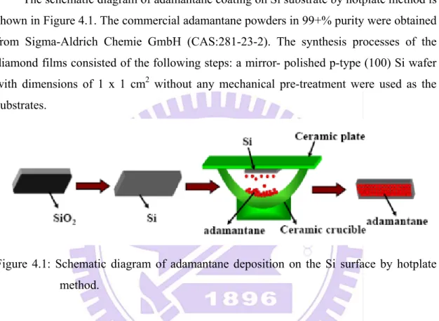
Figure 4.1: Schematic diagram of adamantane deposition on the Si surface by hotplate method --- 52
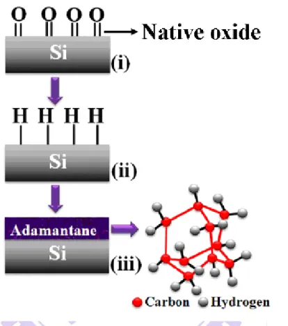
remove native oxide from the Si surface, and (iii) adamantane deposited on
silicon surface by hotplate method --- 53
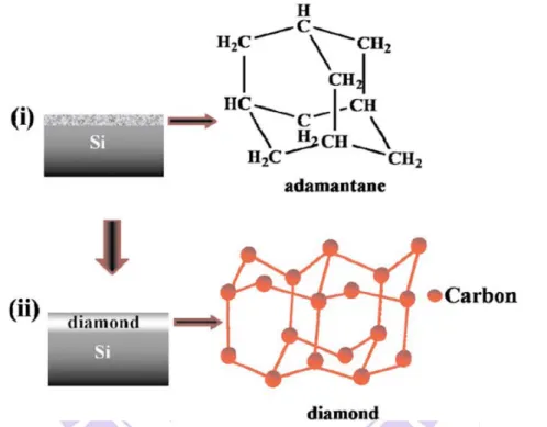
Figure 4.3: Schematic diagram showing diamond synthesis in two steps; (i) adamantane deposited on silicon surface by hotplate method and (ii) diamond growth by MPCVD --- 54
Figure 4.4: Photograph of solid crystalline adamantane powder --- 55
Figure 4.5: (a) Optical image, inset: high-magnification image of the adamantane, (b) XRD pattern of adamantane, and (c) Raman spectrum of the adamantane coating layer on Si (100) substrate --- 57
Figure 4.6: JCPDS file showing the intensity of adamantane peak --- 58
Figure 4.7: Tapping-mode AFM image of adamantane on Si --- 59
Figure 4.8: Photographs of adamantane at high temperature ~ > 400W at 20 torr --- 60
Figure 4.9: SEM image of diamond on AC/Si at 200W after 270 min growth --- 62
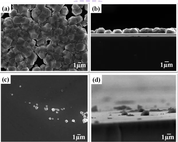
Figure 4.10: (a) low magnification and (b) high-magnification SEM image of diamond on AC/Si at 250 W after 270 min growth --- 62
Figure 4.11: SEM image of diamond: (a) plan-view of AC, (b) cross-section view of AC, (c) plan-view of WAC and (d) cross-section view of WAC --- 63
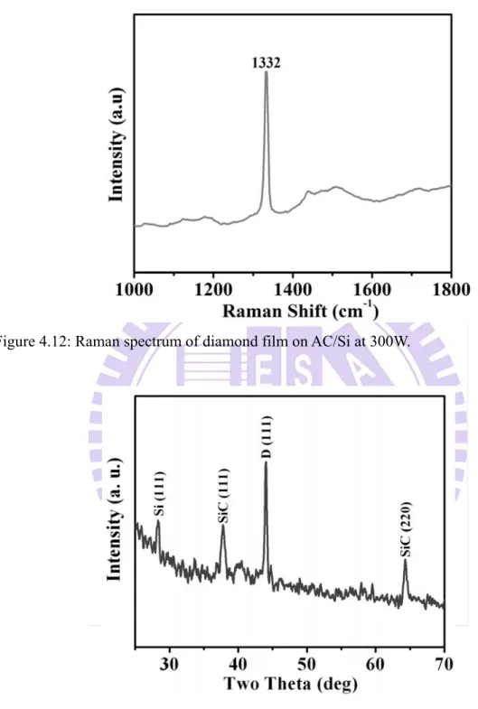
Figure 4.12: Raman spectrum of diamond film on AC/Si at 300W --- 65
Figure 4.13: XRD pattern of diamond (D) film at 300W. The symbol D in this pattern represents diamond --- 65
Figure 4.14: (a) Cross-sectional BF-TEM image of diamond/Si, (b) BF-TEM image of
interface, (c) enlarged BF image of interface; insert EDX spectrum from interface, and (d) SAED pattern of interfacial region indicating the presence of Si and diamond spots {111} plane along <011> direction; Inset diffraction spots (i) and (ii) showing the diamond and Si along <011> Zone
Figure 4.15: The XPS survey spectrum of diamond/Si, insert: high-resolution spectrum
of the C 1s region --- 67
Figure 4.16: SEM images of AC/Si substrates treated with 1, 2, 5, and 10 min by pure
hydrogen plasma at 300W --- 70
Figure 4.17: Raman spectrum of AC/Si treated with pure hydrogen plasma at different
times (1, 2, 5, 10 and 15 min) --- 71
Figure 4.18: Plan-view SEM images and micro-Raman spectra after growth for
deposition times of (a) and (c) 15 min, (b) and (d) 30 min, and (c) and (f) 45 min --- 73
Figure 4.19: (a) Raman spectra from plane regions and (b) XRD patterns of
adamantane-coated Si substrates after 15, 30, and 270 min deposition at 350W --- 74
Figure 4.20: Cross-sectional SEM images of adamantane-coated Si substrates treated
with various times: (a) 15 min, (b) 30 min, and (c) 45 min at 350W --- 75
Figure 4.21: (a) XPS survey spectrum, (b), (c), and (d) high resolution spectrum of the
C(1s) region after 15, 30 and 45 min deposition --- 77
Figure 4.22: Photographs of CVD plasma (a) at 60 and (b) at 300 sec --- 79 Figure 4.23: SEM image and Raman spectrum after 30 min growth on WAC/Si at 350W
--- 81
Figure 4.24: Plan-view and cross-sectional SEM images of diamond after 270 min
growth on WAC/Si substrate at 350W --- 82
Figure 4.25: SEM images of deposited diamond in (a) plan–view: inset high
magnification of diamond and (b) cross-sectional view, inset: high-magnification image of interlayer after synthesized diamond (growth time 270 min) on AC/Si at 350W --- 84
Figure 4.27: (a) AFM and (b) corresponding Raman spectrum of plane region where we
did not observe microdiamond film after 270 min diamond growth --- 86
Figure 4.28: The XPS survey spectrum of diamond/Si, inset: high resolution spectrum of
the C 1s region --- 87
Figure 4.29: (a) Cross-sectional BF-TEM image of diamond/Si, (b) SAED pattern of
interface between Si and diamond, (c) SAED pattern of diamond {111} plane along <110> direction, (d) High-resolution TEM lattice image of diamond; the d-spacing between the fringes was ~ 2.04 Å, which was identified {111} diamond lattice plane --- 88
Figure 4.30: Emission current density as a function of applied electrical field for
diamond plates and inset corresponding F–N plot --- 90
Figure 5.1: Schematic diagram showing diamond synthesis in five steps; (a) silicon
substrate with native oxide layer, (b) Pt coated on SiO2/Si substrate by sputtering process, (c) Pt/SiO2/Si immersed into hexane+adamantane solution, (d) adamantane deposited on Pt/SiO2/Si surface by ultrasonication, and (e) diamond growth by MPCVD --- 94
Figure 5.2: Photographs of (a) adamantane (100mg)+(5ml) hexane solution, (b)
Pt/SiO2/Si dipped into solution, and (c) ultrasonication process for adamantane deposition --- 95
Figure 5.3: (a) plan-view SEM image; insert high magnification image, (b) cross-section
view, (c) FTIR spectrum, (d) Raman spectra, (e) x-ray diffraction pattern, and (f) AFM image of adamantane on the Pt/SiO2/Si after ultrasonic process -- 97
Figure 5.4: Top-view SEM images of (a), (b), (c) after 2 min and (d), (e), (f) after 5 min
growth on adamantane/Pt/SiO2/Si --- 99
Figure 5.6: Cross-sectional view SEM images of (a) after 2min, (b) after 5 min, (c) after
10 min, and (d) after 15 min growth on adamantane/Pt/SiO2/Si --- -101
Figure 5.7: (a) Cross-sectional SEM of deposited adamantane/Pt/Si with the
corresponding nanobeam Auger electron mapping of (b) Carbon, (c) Platinum, and (d) Silicon --- 102
Figure 5.8: Plan-view SEM images of (a) and (b) after 2 min, (c) and (d) after 5 min, (e)
and (f) after 10 min, (g) and (h) after 15 min growth on adamantane/SiO2/Si (without Pt) --- -103
Figure 5.9: Raman spectra of (a) adamantane-seeded Pt/SiO2/Si (with Pt) and (b) adamantane-seeded/SiO2/Si (without Pt) after 2, 5, 10, and 15 min treated with 1% CH4 in H2 at same experimental conditions --- -104
Figure 5.10: Plan-view SEM images of (a) and (b) after 5 min, (c) and (d) after 15 min,
treated with pure hydrogen plasma on adamantane/ Pt/SiO2/Si --- -106
Figure 5.11: (a) XPS survey spectrum of adamantane/Pt/SiO2/Si (b), (c), (d), and (e) high-resolution spectrum of the C (1s), and (f) high-resolution spectrum of the Pt (4f) region after various time treatments --- -107
Figure 5.12: (a) XPS survey spectrum of adamantane/Pt/SiO2/Si, (b) high-resolution spectrum of the C (1s), and (c) high-resolution spectrum of the Pt (4f) region after 5 min treatment with pure hydrogen plasma --- -108
Figure 5.13: (a) Plan-view SEM, (b) high-magnification SEM image, (c) cross-sectional
SEM image, (e) XRD pattern, and (f) Raman spectra of diamond (growth time 2 hr) on Pt/SiO2/Si (d) Plan-view; insert high magnification image of diamond on without Pt --- -110
Figure 5.14: The XPS spectra (a) survey spectrum, (b) high-resolution spectrum of the C
Figure 5.14: (a) Cross-sectional BF-TEM image of diamond/Pt/Si (b) HRTEM lattice
image of diamond/Si; the d-spacing between the fringes was ~ 2.06 Å of diamond {111} plane; the inset showing FFT patterns from of Si and diamond lattice images (indicated by arrow), and (c) SAED from (rectangle marked region) of diamond along <110> direction --- -114
Figure 5.15: EDX spectra of inset mark in B.F image in Figure 5.15 (1) From Pt
interface particles, (2) without Pt particles in the interfacial region, (3) Si substrate, and (d) from diamond particles --- -115
Figure 5.16: Schematic diagram of diamond growth on adamantane seeded Pt/SiO2/Si substrates --- -116
Chapter 1
Introduction
1.1 Background
Diamond has always been an outstanding and desirable material. Not only is it famous to the public as gemstones, but also it is attractive to scientists and engineers for its unique, excellent properties. The outstanding electrical, optical, mechanical, chemical, and thermal properties of diamond film have stimulated a great deal of research activities in the growth of diamond thin films using various chemical vapor deposition (CVD) techniques, to study its growth mechanisms, and their wide range of potential applications for optics, microelectronics, tribology, thermal management, DNA sensors, and so on. From the crystal growth viewpoint, synthesis of diamond thin films by CVD in vacuum is a breakthrough in artificial diamond growth compared with using the high temperature and high pressure (HTHP) method [1]. Over the past few decades, different techniques have been developed for the deposition of diamond such as chemical vapor deposition (CVD), pulsed laser deposition, ion beam deposition hydrothermal growth, and oxyacetylene torch or combustion flame method [2-8]. Among all these methods, chemical vapor deposition (CVD) has become a well-established field over the last three decades. CVD diamond materials range in grain size from ultrananocrystalline and nanocrystalline [9, 10] films, through polycrystalline plates and wafers [11], to large single crystals [12, 13]. Ultrananocrystalline diamond (UNCD) is a new special class of nandiamond that has a length of only few nanometers. Due to superior properties of UNCD, the ultrananocrystalline diamonds is most suitable for future biochip and biosensor applications. Nanocrystalline diamond coatings are also promising for certain medical implants such as cardio vascular surgery or coating of certain components of
particularly microwave plasma-activated CVD (MPCVD), has become dominant in both industrial and research facilities worldwide for high-quality diamond deposition. A large variety of carbon-containing gases can be employed, including methane, aliphatic and aromatic hydrocarbons, alcohols, ketones, amines, ethers, and etc [15]. Methane is the most frequently used reagents for diamond growth.
Recently, a number of surface pretreatment methods have been developed, including scratching [16], seeding [17, 18], electrical biasing [19], and chemical pre-treatments [20], to improve substrate surface conditions prior to diamond deposition. The scratching and seeding substrate surfaces with diamond powders was very useful for increasing diamond nucleation density. Other forms of carbon, including carbon ions, C60 and C70 clusters, amorphous carbon, graphite, thin metal coating, and etc. have also been used as a precursor material in various chemical vapor deposition (CVD) methods under low pressures [21, 22].
1.2 Motivation
Recently, substantial attention has been paid to the development of diamond films on non-diamond substrates in particular using methane and hydrogen gases in the CVD plasma. Although the diamond film synthesized to an extent, some problems remain unclear and only their solution can result in wide-scale commercialization, especially as the synthesis of diamond at low temperature and pressure for the non thermal stable substrates. The most important problem is the synthesis of diamond at low temperature and pressure without sacrificing their quality, purity, yield, and so on.
In general, the good quality of diamond film is synthesized at 1% methane in hydrogen as source gas, 700-1000°C deposition temperature and gas pressures in the range 20-300 Torr [23]. However, the high substrate temperature limits the use of
diamond films in many industrially important systems such as electronics substrate. Deposition of diamond at low temperature is desired for technological applications to allow incorporation of the film into electronic and mechanical devices without damage. There have been several reported works for diamond deposition at low temperature and pressure but they are unsatisfactory at the present stage. Therefore, it would be desirable from both scientific and technological points of view to control not only temperature and pressure but also their quality of diamond. This will permit the use of a much wider range of substrate materials of industrial importance such as Al, polyimide, Si, SiC, GaN, GaAs, steel, Ni, and so on in different mechanical, electrical, optical and electronic applications. Lowering of substrate temperature during diamond synthesis could be an important step for deposition on low melting materials as well.
It is well known that for diamond deposition on non-diamond substrates is performed via two major processing steps. The first one, (i) nucleation, corresponds to the formation of diamond nuclei at the substrate surface. Nucleation procedures have been developed by performing either ex situ treatments on the substrate such as scratching, seeding, chemical treatments, or in situ methods before CVD (chemical vapor deposition) growth such as bias-enhanced nucleation (BEN) process. While the first technique leads to non-uniformity while the bias is limited by the conductivity of the substrate. A uniform nucleation throughout the substrate surface along with its density affects the subsequent growth stage. Therefore, we need to find some new and commercially available precursor for the synthesis of diamond at low temperature and pressure. It is also essential to improve the yield purity, and quality of diamond at low temperature and pressure. Chemical precursor is one of the best ways to overcome this problem. It can improve the quality and enhance the diamond yield without damaging the surface. Moreover, an appropriate synthetic route ultimately determines
applications of materials are heavily dependent upon their synthetic method. As a result, there have been tremendous efforts toward the development of new synthetic methodologies for several decades.
In this study, we have proposed very simple and new methods for pretreatment of the Si surface. We used non toxic chemical precursor such as adamantane (C10H16) for the synthesis of diamond film by microwave plasma chemical vapor deposition (MPCVD) at low temperature and pressure. Prior to the pretreatment, the substrates were not mechanically abraded/scratched. Adamantane was coated on silicon surface by hotplate method and then external methane and hydrogen gas used for diamond growth. The experimental results have shown that the synthesized diamond films are in high yield along with good quality at low temperature. Moreover, noble materials adsorb the hydrocarbon. Therefore, using platinum thin interlayer can enhance the diamond density.
Chapter 2
Literature Review
Carbon is an important element in nature and its allotropes include the hardest naturally occurring substance are the tetragonal bonded (sp3) diamond and also one of the softest substances are the trigonally bonded (sp2) graphite graphite trigonally bonded (sp2). With recent advancement in nanotechnology, new structure of carbon and synthetic production of diamond [24], fullerenes (C60)[25], carbon nanotubes[26], carbon
fibers[27], diamond-like carbon[28], diamondoid hydrocarbons[29], as well as the development of graphene[30] are few examples of this continuously expanding research area.
This thesis concentrates specifically on the lower diamondoid hydrocarbons (particularly on adamantane) to the diamond growth. The following chapter and contents is a brief introduction to the study of diamond and related materials, particularly focusing on the topics mentioned above. As we brief discussed above about the various structure of carbon, however, now we are going to discuss about graphite and diamond.
2.1 Graphite
The mineral graphite is one allotropes of carbon. Graphite has a sheet like structure where the atoms all lie in a plane and are only weakly bonded to the graphite sheets above and below, as shown in Figure 1(a). While, diamond has a framework carbon structure where the carbon atoms are bonded to other carbon atoms in three dimensions (3D). In the diamond lattice structure, hybrid sp3 orbital forms strong covalent bonds with
four neighboring carbon atoms, tetrahedrally arranged with equal angles of 109° 28’ to each other. This three-dimensional network of covalent bonds gives diamond its unique hardness and resistance to wear. Unlike the tetrahedral arrangement of atoms in diamond, the carbon atoms in graphite are arranged in the form of hexagonal rings in layers. In the graphite crystal structure, each carbon atom combines with its three neighbors by sp2
Figure 2.1: Structure of (a) graphite and (b) diamond.
Table 2.1: Comparison of the bond strengths, crystal structure, transparency, thermal conductivity, and electrical resistivity of diamond and graphite [31, 32].
Property Diamond Graphite
C-C bonding Bond Energy Crystalline form Transparency Thermal Conductivity (W/m.K) Electrical resistivity (Ω cm) Covalent sp3 711 kJ/mol Cubic and hexagonal From UV to IR range
~2000 1014
Covalent sp2 and Van der Waals 524 kJ/mol and 7 kJ/mol Hexagonal and rhombohedral
Opaque < 4182(//) and 2(┴)
The carbon-carbon bonds in the graphite mineral are actually quite stronger than those in diamond (Table 2.1). Graphite and graphite powder are valued in industrial applications for its self-lubricating and dry lubricating properties. Graphite is a soft, opaque, lubricious material while diamond is hard, transparent and abrasive. This difference in properties of these materials is determined by the nature of the chemical bonds and structure. There is a common belief that graphite's lubricating properties are solely due to the loose interlamellar coupling between sheets in the structure. The properties of graphite are highly anisotropic. Graphite can conduct electricity due to the vast electron delocalization within the carbon layers. Graphite is able to conduct electricity due to the unpaired fourth electron in each carbon atom. The structure of diamond and graphite are shown in Figure 2.1 and some interesting properties of diamond and graphite are summarized in Table 1. This unpaired 4th electron forms delocalised planes above and below the planes of the carbon atoms. These electrons are free to move, so are able to conduct electricity. However, the electricity is only conducted within the plane of the layers. However, no electronic pathway exists between adjacent graphene layers since the 3.35 Å spacing between graphene layer planes acts as an electrically insulative “vacuum” to electron transfer. The thermal conductivity perpendicular to the planes is very low by comparison due to the weak van der Waals bonding, as shown in Table 2.1. For this reason, graphite is not conductive between layers (parallel with “c” crystallographic axis). There are three principal types of natural graphite:—lump, crystalline, and amorphous. Lump graphite occurs in veins and is believed to be hydrothermal in origin. It is typically massive, ranging in particle size from extremely fine to coarse, platy intergrowths of fibrous or acicular crystalline aggregates with the long axis parallel to the enclosing wall rock. Crystalline flake graphite consists of isolated, flat, plate-like particles with angular, rounded, or irregular edges. It is usually found in layers or pockets in metamorphic rocks. In some deposits, the flake graphite occurs as massive accumulations in veins, lenses, or pods. And amorphous graphite is formed by the thermal metamorphism of coal. The designation amorphous is a misnomer. Its relatively low degree of crystalline order and very fine particle size make it appear amorphous. It is usually of lower purity than the crystalline flake graphite and, therefore, commands a lower price than its more ordered counterpart [33].
Figure 2.2: Photographs of different kind of graphite [http://en.wikipedia.org/wiki/Graphite].
2.2 Diamond
Diamonds were first mined in India over 4000 years ago. For centuries diamonds have captured the hearts and minds of millions, including scientists. For most, the word diamond immediately relates to a brilliant gem, wealth, status and/or prosperity. For scientists, diamond is known as one of the strongest and most chemically inert material. Diamond is something superb, the peerless "king of gems" that glitters, dazzles, and symbolizes purity and strength. The structure of diamond is shown in Figure 2.1(b). It can be regarded as a 3D network of carbon atoms tetrahedrally bonded by sp3
Figure 2.3: Theoretically predicted phase diagram of carbon [http://en.wikipedia.org/wiki/Diamond]. hybridized bonds. Since each carbon atom in the diamond lattice is firmly “supported” by four neighboring atoms, this structure makes the extreme properties of diamond. The extreme properties of diamond such as high mechanical strength, exceptional chemical inertness, outstanding thermal stability, and many other excellent properties made it as a supreme material for diverse applications [34, 35]. Despite being harder and denser than graphite, under ambient conditions, diamond is less stable by 2.9 kJ/ mole. Fortunately, a large activation barrier prevents an appreciable rate for interconversion from diamond to graphite. Since diamond is only metastable at standard temperature and pressures, the production of diamond from other forms of carbon is difficult. Before progressing further let us discuss how diamonds are formed in some more detail.
2.2.1 Natural production
Figure 2.1 (b) shows the structure of diamond. Diamond is the stable solid form of carbon at high pressure. Diamonds are formed deep inside the earths interior where crushing pressure and blistering heat work together for a long period of time to create the diamond lattice. At depths below 150-200 km, the pressure and temperature are such that diamond becomes the most thermodynamically stable form of carbon. Scientists believe that, narrow volcanic pipes running down into the earths interior allows diamonds to be transported via violent explosions to the earth’s surface. It is believed the time taken to form a natural diamond is approximately billions of years.
2.2.2 Synthetic production
Apart from being the hardest known naturally occurring material till presently, diamond also enjoys several other superior properties. Diamond has very high wear resistance and a low coefficient of friction. Diamond is also inert to most chemical environments and hence diamond coatings can be used for corrosive and/or corrosion-erosion applications as well. It is also a bio-compatible material. The high carrier mobility [36], wide band gap and thermal stability [37] of diamond means that electronic devices would be able to operate faster and under much more extreme conditions than silicon based devices. It has very low thermal expansion coefficient at room temperature. Diamond also has low or negative electron affinity [37]. By virtue of these commendable properties, diamonds have a potential for wide ranging applications for wear and corrosion resistant applications, field emission, heat sinks, optical windows etc [37]. However the high costs of natural diamonds severely restricts their application potential. Scarcity and cost of the natural diamond led scientists to find means of making diamond in the laboratory. Although there have been several attempts to synthesize diamond from various sources of carbon since it was discovered to be an allotrope of carbon, two main techniques were invented in 1950; (i) High pressure and high temperature (HPHT) synthesis and (ii) chemical vapor deposition (CVD) synthesis.
2.2.2.1 High-Pressure High-Temperature Synthesis
With the realization in the nineteenth century that natural diamonds are produced deep under the earths crust under conditions of high temperature and high pressure, scientists started experiments to imitate this condition in laboratories. The first success in synthesising diamond particles by HPHT probably belongs to Swedish in about 1953 and in the Unites States by General Electric in 1955 [24]. They used pressures of 10 GPa and temperatures in excess of 2300 K to produce diamond crystals with an edge length of over 1 mm. HPHT, a process which mimics the way in which natural diamonds are formed by geophysical processes deep in the earth, has allowed synthetic diamond to become a key material in the cutting and abrasive business, being widely used in the machine tool industry, oil and gas drilling, mining, quarrying, and construction. Over the years the process has been refined, and it is now possible to produce different types of diamonds of several carats in mass [38]. It can be seen from the carbon phase diagram (Figures 2.3 and 2.4) that the diamond structure is stable at very high temperatures and pressures. Today, the diamond synthesis by HPHT process remains the dominant manufacturing process for industrial diamond, as shown in Figure 2.5.
Figure 2.4: Carbon phase diagram with temperature and pressure ranges corresponding to various diamond synthesis process [39].
2.2.2.2 Shock-wave Synthesis
Figure 2.6 shows the schematic diagram of Shock-wave for diamond synthesis. Shock-wave synthesis methods are better than traditional HPHT methods. These methods only produce small grain size (nano) diamond powders. In 1961, Decarli et al. had observed diamond from graphite after explosive shocks at 300,000-atmosphere and Greiner et al also noticed diamond crystals with soot after the detonation of carbon-containing molecules at high explosive in an inert atmosphere [40, 41]. The nanocrystals of diamond are formed by shock-wave synthesis due to the incredibly short reaction time [42].
2.2.2.3 Chemical Vapor Deposition (CVD)
Synthesis of diamond by Chemical Vapor Deposition (CVD) uses a low pressure process. This technology opens the possibility of making new shapes, coatings, films and qualities that can exploit diamond’s unique properties in a breath-taking array of industries. The possible growth of diamond by CVD was first shown by Angus et al. in 1968 [44]. It is a process which includes both gas phase reactions and gas-solid surface reactions. The process relies on decomposing carbon-containing gas molecules, such as methane, acetylene or carbon dioxide at sub-atmospheric pressure and depositing diamond as a film on a substrate. Figure 2.7 shows the appropriate ratio of each elements such as C, H, and O for the diamond growth [45]. The importance of CVD methods is that they do not require the huge pressures required for HPHT synthesis and can create diamond that can be tailored for a wide range advanced engineering applications.
Figure 2.7: The Bachmann Diagram [45]. This diagram shows the relative proportions of C, H, and O required in the gas phase for CVD diamond growth to occur.
Recently, there are four main CVD methods used to create diamond films. The CVD techniques, classified by means of how the energy is coupled into the system (called gas activation), which will be briefly introduced in the following sections.
2.2.2.3.1 Hot filament
Figure 2.8: (a) Schematic and (b) Photograph of hot filament CVD reactor[http://www.chm.bris.ac.uk/pt/diamond/end.htm].
In 1976, Soviet scientists have successfully diamond synthesized on non-diamond substrates by hot filament CVD (Hot Filament Chemical Vapor Deposition, HFCVD). The schematic diagram of HFCVD is shown in Figure 2.8. It uses a metal coil, resistively heated to around 2000~2500 K to activate the gas phase reactions. In the HFCVD, normally researchers are using the mixture of methane and hydrogen. The filament works as a power source and catalyst at the same time to help dissociate the H2. The resulting H
atoms then initiate most gas phase reactions with the hydrocarbon and finally lead to diamond deposition on the Si substrate, which is heated separately by an electric heater to 1000~1200 K. Therefore, the properties of the filament are very important for HFCVD. The commonly used filament material is a kind of chemically-inert metal, e.g. tungsten or tantalum. However, under the high temperature, it will inevitably react with carbon-containing species and gradually degrade, and finally become more brittle and resistive. This then will influence both the power coupling efficiency and the catalysis activity.
contain oxidizing or corrosive gases. Even so, the contamination from the filament material is still difficult to avoid. Thus, usually, HFCVD-grown diamond has low quality and is suitable for mechanical, but not for electronic applications.
2.2.2.3.2 Arcjet plasma
Figure 2.9: (a) Schematic and (b) Photograph of a DC arcjet reactor[http://www.chm.bris.ac.uk/admin/tpw.htm].
The DC arcjet is another CVD method to produce diamond. The schematic diagram of Arcjet plasma is shown in Figure 2.9 In this system, an anode and a cathode are connected by a DC power supply. Between the two electrodes a discharge region is formed. When the mixture of gases flow through this region, ionization occurs and a jet of plasma is generated and accelerated by a pressure drop towards the substrate, where the diamond film is deposited. The advantage of this technique is its high growth rate, which is usually unobtainable by other methods. The maximum can be 1mm/hr [47]. However, this method cannot grow diamond over large areas and, again, metal contamination (from the cathode) tends to impair the diamond purity and quality.
2.2.2.3.3 Microwave plasma
Microwave plasma is now the most popular way to produce high quality diamond film. The two most common types of MWCVD reactor are shown in Figure 2. 10. The first microwave plasma CVD reactor was designed at NIRIM [32] using quartz tube of 45-55 mm in diameter that perpendicular penetrates the waveguide for 2.45 GHz, as schematically in Figure 2.10 (a). By this reactor a diamond film coating is possible on a 1-inch Si wafer at maximum, but in most cases, a piece of Si that is only less than 1 cm2 is used as the substrate. In contrast, uniform diamond film coating on large area (2-inch square) is possible using an ASTeX-type reactor, which is shown in Figure 2.10 (b). In a microwave reactor, the gases mixture is introduced. The microwave power is coupled into the chamber through a quartz window. Firstly, electrons will pick up energy from the electromagnetic field. Then, through their collisions, the energy is transferred to the heavy species, making them dissociated, excited or ionized. The “active” species so produced then react on the substrate surface and form the diamond film. The advantage of this method is that there is no electrode or filament in the reactor. This provides a clean environment for diamond growth. Also, the diamond growth rate is relatively fast due to high input power and the immersion of the substrate into the plasma. The main drawback is that such systems are usually expensive. Therefore, we are now entering a new phase for CVD diamond where companies are exploring a raft of new applications. Improvements in plasma-type CVD processes are allowing the growth of polycrystalline and single crystal CVD diamond films with fewer defects and with consistent characteristics.
Figure 2.10: Schematic diagram of (a) NIRIM type [48] and (b) ASTEX type microwave reactor [http://www.chm.bris.ac.uk/pt/diamond/stuthesis/chapter1.htm].
2.3 Properties and applications of diamond
The synthetic diamonds are manufactured in a laboratory by various processes (as described above) for more than half a century. However, in recent years it has become possible to produce gem quality synthetic diamonds of significant size. The large size, high thermal conductivity, low thermal expansion, and low dielectric constant of diamonds makes them excellent as heat sinks [37]. As stated above, they are also the substrate of choice for homoepitaxial diamond CVD. Microcrystalline CVD diamond films are the most versatile form of synthetic diamond. They can be used as protective coatings, for heat dissipation, and even as windows in fusion reactors [37, 49, 50]. The high surface roughness of microcrystalline diamond (MCD) is not well suited for optical, wear and thermal management applications. However, nanocrystalline CVD diamond (NCD) films are increasingly studied due to their smooth surface and relatively homogeneous structure compared to MCD films. The low surface roughness of NCD is being used in optical coating, wear and thermal management applications. The low abrasiveness and antiwear properties of nanodiamond powders make them promising solid lubricants [37]. Moreover, NCD films not only being smooth but also being more adaptive to the CVD diamond applications and having enhanced electronics and other properties. This is reflected in their cost effective and superior performances in the areas of protective coating, tribology, SAW devices, and micro-electronic mechanical devices (MEMS), as shown in Table 2.2. One of the most interesting properties of diamond is the negative electron affinity of the hydrogen-terminated surface [51]. A negative electron affinity implies diamond could be used as a cold cathode in electron emitting devices. Indeed, nanodiamond powders have been shown to produce stable electron emission, with low turn-on voltages (3.2 V/μm) and high current densities (~95 mA m2 under the applied field of 5 V/μm) [52]. Moreover, as the size of grains in changing from micrometer to nanometer, a factor of a million in volume, new properties have started emerging, exploring new areas of applications [37], for example, in X-ray optics, X-ray physics, particle physics, and so on.
2.4. Nucleation and growth of diamond in CVD
2.4.1 Nucleation
The diamond nucleation on the non-diamond substrates is usually very difficult and thus growth of diamond is very slow. Because of very low nucleation density, only of the order of 104 cm-2 on non-scratched substrates [53] is observed. Therefore, unlike diamond substrate, a non-diamond substrate often needs a pretreatment prior to diamond deposition. Several surface pretreatment methods have been developed, such as manual scratching, ultrasonic abrasion, and bias enhanced nucleation, and so on. The substrate scratching was found to be most simple, yet very powerful method for achieving a high nucleation density and uniform grain size. Substrate seeding can be achieved by applying the ultrasonic abrasion technique using a mixture of diamond powder and alcohol. In this method we can achieve a 108 cm-2 diamond nucleation density. The diamond powder was
mixed with Cu, Al2O3, Ti, Fe, c-BN. TaC, and SiC, diamond nucleation enhanced ~109 to
~1010 cm-2 [54]. Nucleation enhancement by scratching is attributed to a number of factors. One of them is the change in the surface morphology due to the formation of defects, breaking of a number of surface bonds and removal of surface oxides. The defects are suggested to be chemically active sites, which preferentially adsorb precursors (diamond) and thus accelerate the nucleation process. Another opinion is that residual fragments of diamond powder act as nuclei for the diamond growth during CVD deposition. This is known as the seeding effect. Unfortunately, these abrasion techniques cause considerable damage to the surface and hence are not practical for electronic device applications. In contrast to the commonly used scratch methods, bias enhanced nucleation pretreatment does not cause mechanical damage to the substrate but still can induce a high nucleation density. The bias treatment is an in-situ method, where plasma is generated by biasing the substrate positively and negatively with respect to the chamber prior to the growth stage. This method is only good for semiconductor and conductive substrates. In 1991, Yugo et al. had successfully increased diamond nucleation by bias treatment [55]. There have two types of bias (i) negative bias and (ii) positive bias. In the negative bias, the positively charged ions in the growth chamber are accelerated towards the surface and bombard it, thereby removing the contamination and facilitating cluster
formation on the surface, as shown in Figure 2.11 (a). While Figure 2.11 (b) shows the positive bias effect where negative electrons are adsorbed and impact on the substrate and carbon atoms. Figure 2.12 shows the schematic diagram of bias enhancement nucleation and epitaxial growth of diamond.
2.4.2 Diamond growth mechanism
For the diamond deposition, various types of carbonaceous gases as sources were investigated for their potential on CVD diamond deposition, such as CH4, C2H6, C2H2,
C2H4, CO, CH3OH, C3H6O, CCl4, and CCl2F2. However, in present work, methane gas
was used as a source gas [54]. The chemistry behind the diamond growth is very complicated. It can be divided into gas-phase chemistry and surface chemistry.
2.4.2.1 Gas phase chemistry
A general schematic of the CVD diamond deposition process is shown in Figure 2.13. It is believed that hydrogen atoms usually play a crucial role in initiating the relevant gas phase reactions [58]. In a CVD diamond deposition process, when a H2 and
CH4 mixture is introduced into the reactor, H2 is dissociated by collisions. This results in
an H-abundant environment. Under high atomic hydrogen concentration, CH4 reacts with
H through a series of abstraction reactions, producing many radicals like CH3, CH2, CH,
C, and etc. These can also react with one another through “self-scavenging” reactions, producing C2 species, like C2H6. Then, following similar H abstraction reactions, species
like C2H5, C2H4, etc are also formed. Among them, C2H2 is the thermodynamically
favored hydrocarbon species. Some of the species will act as precursors for diamond growth in the following gas-solid surface interactions.
2.4.2.2 Surface Chemistry
The H atoms also play an important role in surface reactions. During the surface reaction diamond and non-diamond carbon phases are formed. Graphite phases on the surface are simultaneously etched by hydrogen. Hence, atomic hydrogen plays a very important role in the formation of diamond and in preferential etching of non-diamond carbon phase. They can continuously create and re-terminate (thereby preventing the reconstruction to non-diamond forms) the reactive surface sites necessary for the propagation of the diamond lattice sites. H atoms can also selectively etch any graphitic (sp2) carbon through so-called β-scission processes [59], as shown in Figure 2.14.
Figure 2.14: Two β-scission processes to attack a surface-bonded ethyl group [59]. Cd
represents the carbon atom on the diamond surface.
Figure 2.15: The GDSB mechanism for methyl insertion [59].
Recently, C1 and C2 mechanisms are two accepted mechanisms for diamond growth. In C1 mechanisms (Figure 2.15), the usually assumed growth species is CH3 due to its
abundance in the gas phase. In 1992, Garrison, Dawnkaski, Srivastava, and Brenner suggested a so-called GDSB mechanism, as shown in Figure 2.15 for methyl addition to
the (100) surface [60]. While in C2 mechanism is shown in Figure 2.16 for the addition of acetylene to the (100)-(2×1):1H surface [58, 61].
Figure 2.16: C2 mechanism for the addition of acetylene [58, 61].
2.5 Diamondoid Hydrocarbons
Diamondoids are saturated hydrocarbons and its molecules are totally or largely super imposable on diamond lattice [62]. Adamantane (C10H16) is a cycloalkane and also
a lowest unit of diamonoids. The diamondoid can be split into two groups; (i) Diamondoids that are only partly superimposable on the diamond lattice, and (ii) Diamondoids which are completely superimposable on the diamond lattice. The carbon skeleton of adamantane comprises a small cage structure. Because of this, adamantane and diamondoids in general are commonly known as cage hydrocarbons. An additional diamond cage is face-fused to the 10-carbon adamantane structure, a molecule of diamantane (C14H20), and another adamantane fusing with diamantane it forms
trimantane (C18H24) and so on [63]. The higher adamantane molecules (diamantine,
2.5.1 Lower diamondoids
Diamondoid was first discovered and isolated from Czechoslovakian petroleum in 1933 [64]. The isolated substance was adamantane and the name came from the Greek for diamond (adamas). This name was chosen because it has the same structure as the diamond lattice, highly symmetrical and strain free. The rigidity, strength, and assortment of their three dimensional (3D) shapes make them valuable molecular building blocks. The simplest of these polycyclic diamondoids is adamantane, followed by its homologues diamantane, tria-, tetra-, penta- and hexamantane. The lower diamondoids have chemical formulas of C4n+6H4n+12, where n equals the number of diamond-cage subunits [65].
Adamantane was first synthesized in five stages by Prelog in 1941 from Meerwein's ester and had a yield of about 0.16% [66]. Schleyer (in 1957) found 30-40% yield, when he had used catalyst and then this method become an affordable source of adamantane [67]. The two cage structure (Diamantane) was first produced in 1965 by Cupas et al. [68], although it was isolated from petroleum a year later [69]. While, trimantane was discovered in 1966 [70], however, the synthesis of progressive polymantanes (higher diamonoids) became increasingly difficult. The formation mechanism of the higher diamondoids in petroleum remains a mystery. So far, it has not been possible to synthesize higher diamondoids except antitetramantane, a tetramantane isomer. Certain higher diamondoids are now available in multi-gram quantities through Molecular Diamond Technologies, Inc. on a collaborative basis. By comparison, lower diamondoids (adamantane, diadamantane, and triadamantane), extracted from crude oil much earlier than larger members of the diamondoid series, are currently available in kilograms quantities and can be synthesized. Figure 2.17 shows the structures of lower diamonoids in different models such as 3D stick, 3D ball and stick, and 3D space filling models.
Figure 2.17: Structure of lower diamonoids (a) adamantane, (b) diamantane, and (c) triamantane in different models.
2.5.2 Higher diamondoids
After the discovery of lower diamondoids, the higher diamondoids were sought, however, the synthesis of progressive polymantanes (higher diamonoids) became increasingly difficult. In 1955, a group of higher diamondoids, including tetramantane, pentamantane, and hexamantane, was first discovered in a gas condensate produced from a very deep ( 6800 m below the surface) petroleum reservoir located in the US Gulf Coast [71]. These polymantanes and their isomers were identified by gas chromatography/mass spectrometry (GC-MS). In 2003 Dahl et al. [72] published a paper in Science announcing the isolation and crystallization of large selection of higher diamonoids (C22 and higher polymantanes) from petroleum. In total they isolated and
crystallized all four tetramantanes, nine pentamantanes, one hexamantane, two heptamantanes, two octamantanes, one nonamantane, one decamantane, and one undecamantane.
Figure 2.18: Diamondoids isolated; tertamantanes (a,b,c,d), pentamantanes (e,f,g,h,i,j,k,l,m), hexamantanes (n,o,p,q,r,s), heptamantane (t,u), octamantane (v), nonamantane (w), decamantane (x), and the alkylated pentamantane (y) [72].
2.5.3 Properties and applications of lower diamondoids
As we described above that the adamantane is the smallest unit of diamondoids. Adamantane molecule consists of three condensed cyclohexane rings fused in the chair conformation. The carbon-carbon (C-C) bond length is 1.54 Å and is almost identical to that of diamond, and the carbon-hydrogen (C-H) distance is 1.11 Å. The structure of adamantane is shown in Figure 2.19. Adamantane has face-centered cubic crystal structure.
Figure 2.19: Structure of adamantane [http://en.wikipedia.org/wiki/Adamantane].
The density of adamantane at room temperature is ~1.08 g/cm3. The adamantane is a colorless solid crystalline with camphor smell. It is insoluble in water but soluble in hydrocarbon solvents. Adamantane slowly sublimates at ambient temperature and its melting point is ~ at 270 °C [73]. The exact boiling point of adamantane is impossible to be determined due to its sublimation property.
Diamondoids show remarkable rigidity, strength, and thermodynamic stability, as well as interesting electronic properties [74], which may be of use in chemical, polymer, and pharmaceutical applications, as well as in nanotechnology. The adamantane structure is similar to diamond lattice, therefore, adamatane derivative (2-adamantanone) has been used for the nucleation and growth of diamond at 850°C and 40mbar [75]. The SEM image of synthesized diamond is shown in Figure 2.20. The characterization of the synthesized diamond has shown that the quality and crystallinity is good. They also shown that the during diamond deposition silicon carbide (SiC) interlayer formed on the Si substrate [75].
Figure 2.20: (a) SEM image, (b) XPS spectra, and (c) Raman spectrum of synthesized diamond using adamantane derivative for the nucleation and growth of diamond [75].
2.6 Structure of the thesis
The remainder of this thesis consists of six chapters and is organized as follows: In chapter 3, gives a detailed description of the experimental methods and procedures used in this study, and the materials and chemical chosen to accomplish the research work. Chapter 4 shows the diamond deposition at low temperature along with we described that the adamantane first converted into graphitic phase. Further, the graphitic phase acts as a diamond nuclei and its growth. Their excellent field emission property is also shown. While in chapter 5 shows the role of platinum particles. Platinum particles adsorb hydrocarbon (adamantane) and enhances the diamond density. The adsorb hydrocarbon (adamantane) convert into clusters of oriented graphite or carbon crystals in high density. Finally, Chapter 6 gives an overview and conclusions of the present study, and future works.
Chapter 3
Experimental methods
We have developed a several convenient techniques for the synthesis of diamond thin film. The processes include the pretreated Si surface with adamantane (C10H16) by
hotplate method and ultrasonication method for diamond deposition. This chapter contains detailed descriptions of all the experimental techniques and their structure analysis for each process employed in this study.
3.1 Experimental flowcharts
Figure 3.1 shows the experimental flow chart of synthesis and characterization of diamond film on adamantine-coated Si substrates at low temperature and pressure. Prior to diamond film deposition, the adamantane were coated on Si surface by hotplate method.
Figure 3.2 shows the role of platinum (Pt) particles on interface layer for diamond deposition. The admantane deposited on Pt/SiO2/Si layer by ultrasocation process, where
Pt coated SiO2/Si substrate by sputtering process.
In both process (Figures 3.1 and 3.2), diamond films were deposited by 1.5 AsTeX type microwave plasma chemical vapor deposition MPCVD from a gas mixture of methane and hydrogen without the application of a bias voltage to the substrates. In addition, the Si substrates were not mechanically scratched/abraded.
The surface morphology, bonding structure and chemical composition were analyzed by scanning electron microscopy (SEM), transmission electron microscopy (TEM), x-ray photoelectron spectroscopy (XPS), atomic force microscopy (AFM), Raman spectroscopy, x-ray diffraction, Fourier transform infrared spectroscopy (FT-IR), and optical microscopy. The field emission measurements of specimens were performed at room temperature.
Figure 3.1: Experimental flowchart of the synthesis and analysis of diamond film on Si substrate and its application in field emission.
Figure 3.2: Experimental flowchart of the synthesis and analyses of diamond film on Pt/SiO2/Si substrate.
3.2 Substrate holder
We used molybdenum (Mo) holder for diamond growth in all experimental process. The schematic diagram of Mo holder is shown in Figure 3.3.
Figure 3.3: Substrate holder for diamond deposition
3.3 Microwave plasma chemical vapor deposition (MPCVD)
system
The deposition of diamond film was carried out in a microwave plasma chemical vapor deposition system. The photograph of 1.5 kW ASTeX type MPCVD is shown in Figure 3.4 (a). In this system we can increase the power up to 1000W. The schematic diagram of MPCVD reactor is shown in Figure 3.4 (b). The basic structure of MPCVD consists of the following parts, as shown in Figure 3.4 (a):
(i) Microwave generator: The function of microwave generator is to produce microwave. The magnetron in 1.5 ASTeX system generates high frequency (2.45GHz) microwave. (ii) Wave guide: After generating the high frequency microwave, it delivered within square waveguide and finally gets into the microwave chamber through antenna.
temperature and pressure. There is optical quartz glass at the top of chamber while base is made of stainless steel. The unique properties (low microwave absorption coefficient and high thermal stability) of quartz glass are made to use in CVD chamber.
(v) Multi-Gas Controller: It is use to the control the flow of gases into the reaction chamber to generate plasma.
(vi) Pressure Controller and Vacuum System: the function of pressure controller is the control the pressure in the chamber. The vacuum system is mainly dominated by the mechanical pump such as rotary pump.
(vii) Bias System: In laboratory has the additional DC power supply (Model: LABORATORY DC power supply GPR 50H10D) and it can be use in the system as maximum voltage at 450V. The use of positive and negative bias can increase the density and quality of diamonds.
(viii) Cooling System: The main function of this system is to cool the system at room temperature.
Figure 3.4: (a) Photograph and (b) schematic diagram of CVD reactor of 1.5 kW ASTeX type MPCVD system.
Circulator
Multi-Gas
Controller
Mass Flow
Controller
Microwave
Power
Pressure
Controller
Reactor
Chamber
Microwave
generator
(a)
3.4 Material analysis methods
3.4.1 Scanning electron microscopy (SEM)
Scanning electron microscopy (SEM) is used to examine the surface morphology of the samples at a high magnification. The high magnification range of the SEM is achieved due to its resolving power of approximately 3-6 nm. The SEM is useful and popular for many reasons. One of the great advantages of SEM is its large depth of field (the amount of sample that is in sharp focus at one time). This makes it possible to examine surfaces with a relatively high level of surface variability (and at much higher magnifications). This is because the depth of field of the SEM can be up to four hundred times greater than that of a light microscope. Moreover, it has the advantage of easy sample preparation, and high image resolution. A common SEM is equipped with an electron gun to generate an electron beam to be accelerated under 0.4-40 kV voltage. By deflecting the incident beams with scanning coils, a two dimensional image can be obtained by detecting secondary electrons and backscatter electrons.
The microscopes mainly engaged are field emission type SEM JEOL-6500 and 6700. Accelerating voltage is 15 kV with emission current of 10μA. Working distance is 10mm and 8mm under 9.63x10⁻⁵Pa. Here, we used SEM to see the morphology of our films at low and high magnification. We also have taken top-view along with cross-section image.
3.4.2 Micro Raman spectroscopy
Raman spectroscopy is a simple and non-destructive technique for the analysis of carbon materials. Raman spectroscopy has been used to study vibrational, rotational, and other low-frequency modes. In this system, a laser is focused through a microscope onto the specimen and the scattered light is passed to a spectrometer, which is dispersed by the light grating onto a charged coupled device (CCD) detector. The choice of laser wavelength can be varied depending upon the required applications usually from a laser in the visible, near infrared, or near ultraviolet range. The Raman spectra of carbon species is shown in Table 3.1.
We used micro Raman spectroscopy (LABRAM HR 600) with a spatial resolution of the order of 1 μm2 for the analysis of our specimen. In this system, we used Ar and He-Ne lasers with the wavelength of 514.5 and 632.82nm, respectively to the analysis of our specimen. The schematic diagram of the basic working principle of Raman spectrometer is shown in Figure 3.5.
Table 3.1: Raman characteristics of different carbon species of carbon [76].
Wavenumber (cm-1) Different carbon species
1150 1332 1350 ~1450 1580~1600
Nanodiamond or trans-polyacetylene v1-band (C=C)
Diamond (sp3) D-band (sp2)
Trans-polyacetylene v3-band (C=C)
![Figure 2.4: Carbon phase diagram with temperature and pressure ranges corresponding to various diamond synthesis process [39]](https://thumb-ap.123doks.com/thumbv2/9libinfo/8384693.178372/33.892.164.750.161.1006/figure-carbon-diagram-temperature-pressure-corresponding-various-synthesis.webp)
![Figure 2.12: Mechanism of bias nucleation and epitaxial growth of diamond film [57].](https://thumb-ap.123doks.com/thumbv2/9libinfo/8384693.178372/44.892.151.740.222.1002/figure-mechanism-bias-nucleation-epitaxial-growth-diamond-film.webp)
![Figure 2.14: Two β-scission processes to attack a surface-bonded ethyl group [59]. C d](https://thumb-ap.123doks.com/thumbv2/9libinfo/8384693.178372/47.892.179.760.150.863/figure-scission-processes-attack-surface-bonded-ethyl-group.webp)