行政院國家科學委員會專題研究計畫 成果報告
具有金屬閘極與高介電係數閘極介電層之奈米元件之製作
與特性探討
計畫類別: 個別型計畫 計畫編號: NSC94-2215-E-009-068- 執行期間: 94 年 08 月 01 日至 95 年 07 月 31 日 執行單位: 國立交通大學電子工程學系及電子研究所 計畫主持人: 黃調元 計畫參與人員: 盧文泰、盧景森、蔡子儀、詹凱翔 報告類型: 精簡報告 處理方式: 本計畫可公開查詢中 華 民 國 95 年 10 月 13 日
行政院國家科學委員會補助專題研究計畫
■ 成 果 報 告
□期中進度報告
具有金屬閘極與高介電係數閘極介電層之奈米元件之
製作與特性探討
Fabrication and characterization of nano-devices with
metal/high-k gate stack
計畫類別:■ 個別型計畫 □ 整合型計畫
計畫編號:NSC 94-2215-E-009-068
執行期間:94 年 08 月 01 日 至 95 年 07 月 31 日
計畫主持人:黃調元 教授
計畫參與人員: 盧文泰、盧景森、
蔡子儀
、
詹凱翔
成果報告類型(依經費核定清單規定繳交):■精簡報告 □完整報告
本成果報告包括以下應繳交之附件:
□赴國外出差或研習心得報告一份
□赴大陸地區出差或研習心得報告一份
□出席國際學術會議心得報告及發表之論文各一份
□國際合作研究計畫國外研究報告書一份
處理方式:除產學合作研究計畫、提升產業技術及人才培育研究計畫、
列管計畫及下列情形者外,得立即公開查詢
□涉及專利或其他智慧財產權,□一年□二年後可公開查詢
執行單位:國立交通大學電子工程研究所
2
具有金屬閘極與高介電係數閘極介電層之奈米元件之製作與特性探討
“Fabrication and characterization of nano-devices with metal/high-k gate stack”
計畫編號:NSC94-2215-E-009-068 執行期間:94 年 8 月 01 日 至 95 年 7 月 31 日 主持人:黃調元 交通大學電子工程系教授 中文摘要 在 本 研 究 中 , 將 探 討 氟 吸 附 對 於 具 有 HfO2/SiON 閘極介電層之 P 型金氧半場效電晶 體之影響。使用離子佈值打入氟,藉由之後的 雜質活化將氟擴散進去閘極介電層。研究中發 現,氟的採用幾乎沒有影響到電晶體之基本電 性,如臨界電壓、次臨界斜率、閘極漏電流及 等效氧化層厚度。但是,在固定電壓及溫度劣 化處理之後,對於具有氟吸附的元件,有較少 的介面能態產生及較少的電荷捕捉。此外,本 研究中我們首先證實藉由氟吸附能增強電漿 電荷損害之免疫力。 關鍵字:電壓溫度不穩定性、氟(F)、二氧化鉿、 電漿電荷損害。 Abstracts
Effects of fluorine (F) incorporation on the reliabilities of pMOSFETs with HfO2/SiON gate
stacks have been studied in this work. Fluorine was incorporated during the source/drain implant step and was diffused into the gate stacks during subsequent dopant activation. We found that F introduction only negligibly affects the fundamental electrical properties of the transistors, such as threshold voltage Vth,
subthreshold swing, gate leakage current, and equivalent oxide thickness. In contrast, reduced generation rates in interface states and charge trapping under constant voltage stress and bias temperature stress were observed for the
fluorine-incorporated split. Moreover, We demonstrated for the first time that F incorporation could strengthen the immunity against plasma charging damage.
Keywords: Bias temperature instability (BTI), fluorine (F), hafnium oxide, plasma charging damage.
Introduction
Recently, HfO2 has emerged as the leading
high-k dielectric to replace the conventional SiO2. However, a number of pending issues need
to be resolved before HfO2 can be inducted into
the mainstream ultra-large-scale integration (ULSI) technology. These issues include solving mobility degradation and threshold voltage instability, as well as reducing the number of fixed charges and charge traps [1-4]. Although there exist numerous literature reports regarding methods to incorporate nitrogen [5, 6] or Si [7, 8] into Hf-based films or stacks so as to improve the film’s quality, however, to the best of our knowledge, the effect of F incorporation on HfO2 gate dielectric was seldom addressed [9,
10]. In this report, fluorine incorporation through fluorine implantation into the source/drain regions was used to evaluate its impact on the constant voltage stress (CVS) instability and negative bias temperature instability (NBTI) of pMOSFETs with HfO2 gate stacks. Our results
clearly show that these degradations are improved in the F-incorporated samples. Moreover, because few studies [9] have been performed regarding plasma charging effects of HfO2 gate stacks, we have therefore carried out a systematic study in this regard and found that larger antenna ratio will result in much severe degradation. More importantly, our data also show that the plasma charging damage can be significantly improved by the F incorporation into the HfO2 gate stacks.
Experimental
pMOSFETs with HfO2/SiON gate stacks were fabricated in this work. The thin (0.6 nm) interfacial oxynitride layer (SiON) was first grown by rapid thermal processing (RTP) in an N2O ambient at 700°C. Subsequently, a 3-nm
HfO2 layer was deposited by atomic vapor
deposition (AVD) using an AIXTRON Tricent system at a substrate temperature of 500°C. Wafers were then annealed in an N2 ambient at
700°C for 20 s to improve the HfO2 film quality.
Next, a 200-nm polycrystalline silicon (poly-Si) layer was deposited by low-pressure chemical vapor deposition (LPCVD). Then, the gate electrode was patterned through lithographic and etching processes. Some wafers then received a fluorine (F, 2×1015 cm− 2) ion implantation into
the source/drain region without removing the photoresist on the gate electrode. This was deliberately performed to avoid the potential complication caused by fluorine-enhanced boron penetration. After photoresist removal, source/drain regions were formed by regular boron implantation, with the dopants activated at 950°C by rapid thermal annealing for 20 s in an N2 atmosphere. It should be noted that the
thermal budget of dopant activation also served to diffuse the F species into the HfO2 gate stacks.
After passivation layer deposition, contact holes and aluminum metalization were formed. Finally, a forming gas annealing at 400°C was performed for 30 min to complete the device fabrication.
The equivalent oxide thickness (EOT) of the gate dielectric was extracted from high-frequency (100 kHz) capacitance–voltage (C–V) curves at strong inversion without considering the quantum effect. Charge pumping current was measured with fixed amplitude method at a frequency of 1 MHz [11].
Results and Discussion
Fig. 1 depicts the typical Id-Vg curves of
pMOSFETs with HfO2/SiON gate stacks, both
with and without F incorporation. The inset table shows the corresponding transistor parameters. It can be seen that all key device parameters, including the interface state density Nit, EOT, Vth, and gate leakage current, are essentially
indistinguishable between the samples with and without F incorporation. The inset at the upper right corner shows that the distribution of Vth is
not affected by the addition of F. All these data suggest that little or no adverse impact on the fundamental electrical properties is achieved with F introduction.
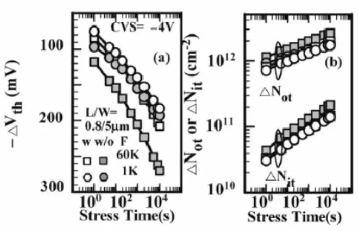
For the reliability evaluation, negative CVS test was performed at 25°C, with the transfer curves measured for monitoring ∆Vth at
various stressing times. The results are shown in Fig. 2(a). To reduce the unstable fast charge detrapping effects [1]–[4], a small positive voltage (0.5 V) with a duration of several seconds was applied to detrap these charges before Id−Vg and charge pumping
4 measurements without inducing extra damage to the gate stacks. This step thus allows much accurate estimation of the slow trap density without the complication due to the interval variation between voltage stressing and parameter measurement. In other words, the precaution allows us to focus on the slow traps in the gate stacks in this work. It is clear that the F-incorporated sample always shows smaller ∆Vth than the control counterpart. To further
gain insights into the degradation mechanism during voltage stressing, the interface state generation ∆Nit and the increase of effective bulk
trap density ∆Not are plotted as a function of the
injection charge density in Fig. 2(b). It should be noted that ∆Not was calculated from ∆Vth by
assuming that the charge was trapped at the interface between the dielectric and the substrate. Apparently, ∆Not was significantly larger than
∆Nit, suggesting that the degradation under CVS
was dominated by the charge trapping in the bulk of HfO2 films, rather than the generation of
interface states, whether fluorine was incorporated or not. Moreover, F incorporation was found being able to suppress the charge trapping in the bulk of HfO2 films. Although
reduced charge injection during stressing was a plausible cause for the observed improvement in the F-incorporated split, it contradicted with the observation that the improvement became more visible with decreasing channel length, as show n in Fig. 3. If the improvement seen in F-incorporated split was indeed due to reduced injection charges, no dependence of the improvement on the channel length should be expected. Therefore, we concluded that the improvement was indeed the result of the F incorporation.
Fig. 4(a) and (b) compares the dependence of threshold voltage shift and the interface generation, respectively, on injection charge density for splits with and without F incorporation. The BT stress condition was Vg = −3.5 V under 125°C. It can be seen that F-incorporated films exhibit NBTI improvement similar to fluorine-induced NBTI improvement in SiOF case[12,13]. The major degradation of NBTI is caused by the positive charge trapping in the films rather than the interface generation, suggesting that the positive charge trapping is not entirely caused by the H+ capturing. Therefore, in addition to positive charge caused by H species, a significant amount of extra trapping centers must be present in the HfO2/SiON gate stack. Fluorine atoms seem to
effectively decorate these trapping centers, leading to reduced degradation
In our process, the photoresist layer that remained after metal patterning was stripped with O2 plasma in a downstream plasma asher,
whose configuration and plasma potential distribution could be found in [14]. Using CHARM-2 wafer sensor, it has been previously shown [14] that the potential distribution was highly negative and positive at the wafer center and edge, respectively. Fig. 5 shows the time evolution of the threshold voltage shift and interface state generation for the devices with area antenna ratios (AARs) of either 1×10³ or 6 × 10⁴, both with and without F incorporation. All measurements were performed on devices located at the same die location (i.e.,wafer center). Fig. 4 shows that the hole trapping in the bulk, rather than the interface generation, is the preponderant mechanism responsible for the degradation. From the Weibull plot of Vth for the
fresh devices located at the wafer center, it is found that the control devices with AAR of 6× 10⁴ depict larger |Vth| values than their
counterparts with F incorporation (data not shown). This is consistent with previous results in CVS and NBTI. Moreover, all these results are in-line with the hypothesis that plasma antenna charging effect creates more hole traps in the HfO2/SiON gate stacks and that
F-incorporated devices are more robust to plasma charging effect.
Conclusions
In this work, we found that the reliabilities of pMOSFETs with HfO2/SiON gate stacks under both CVS and NBTI stresses are significantly improved by the F incorporation. In addition, we demonstrated for the first time that plasma charging effect induces hole trapping in the HfO2/SiON gate stacks. Finally, we found that the plasma charging effect can be effectively suppressed with F incorporation.
References
[1] S. Zafar, A. Callegari, E. Gusev, and M. Fischetti, “Charge trapping related threshold voltage instabilities in high permittivity gate dielectric stacks,” J. Appl. Phys., vol. 93, no. 11, pp. 9298–9303, Jun. 2003.
[2] J. Zhu, T. P. Ma, S. Zafar, and T. Tamagawa, “Charge trapping in ultrathin hafnium oxide,” IEEE Electron Device Lett., vol. 23, no. 10, pp. 597–599, Oct. 2002.
[3] E. P. Gusev and C. P. D’Emic, “Charge detrapping in HfO2 high-k gate stacks,” Appl. Phys. Lett., vol. 83, no. 25, pp. 5223–5225, Dec. 2003.
[4] A. Kerber, E. Carter, L. Pantisano, M. Rosmeulen, R. Degraeve, T. Kauerauf, G. Groeseneken, H. E. Maes, and U. Schwalke, “Characterization of VT instability in
SiO2/HfO2 gate dielectrics,” in Proc. 41st Int. Reliab. Phys. Symp., Dallas, TX, 2003, p. 41. [5] C. S. Kang, H. Cho, R. Choi, Y. Kim, C. Y.
Kang, S. J. Rhee, C. Choi, M. S. Akbar, and J. C. Lee, “The electrical andmaterial characterization of hafnium oxynitride gate dielectrics with TaN-gate electrode,” IEEE Trans. Electron Devices, vol. 51, no. 2, pp. 220–227, Feb. 2004.
[6] C. S. Kang, H. Cho, K. Onishi, R. Choi, Y. H. Kim, R. Nieh, J. Han, S. Krishnan, A. Shahriar, and J. C. Lee, “Nitrogen concentration effects and performance improvement of MOSFETs using thermally stable HfOxNy gate dielectrics,” in IEDM Tech. Dig., 2002, pp. 865–868.
[7] T. Iwamoto, T. Ogura, M. Terai, H. Watanabe, N. Ikarashi, M. Miyamura, T. Tatsumi, M. Saitoh, A. Morioka, K. Watanabe, Y. Saito, Y. Yabe, T. Ikarashi, K. Masuzaki, Y. Mochizuki, and T. Mogami, “A highly manufacturable low power and high speed HfSiO CMOS FET with dual poly-Si gate electrodes,” in IEDM Tech. Dig., 2003, pp. 639–642.
[8] Y. Kim, H. J. Lim, H. Jung, J. Lee, J. Park, S. K. Han, J. H. Lee, S. Doh, J. P. Kim, N. I. Lee, Y. Chung, H. Y. Kim, N. K. Lee, S. Ramanathan, T. Seidel, M. Boleslawski, G. Irvine, B. Kim, H. Lee, and H. Kang, “Characteristics of ALD HfSiOx using new Si precursors for gate dielectric applications,” in IEDM Tech. Dig., 2004, pp. 511–514.
[9] H.-H. Tseng, M. E. Ramon, L. Hebert, P. J. Tobin, D. Triyoso, S. Kalpat, J. M. Grant, Z. X. Jiang, D. C. Gilmer, D. Menke, W. J. Taylor,Adetutu, and B. E. White, “Threshold voltage instability and plasma induced damage of poly-Si/HfO2 devices -positive impact of deuterium incorporation,” in Proc. ICICDT, 2004, pp. 255–259.
[10] A. Mineji, Y. Tamura, T. Watanable, H. Ozaki, F. Ootsuka, T. Aoyama, K. Shibata, K. Tsujita, N. Ohashi, M. Yasuhira, and T. Arikado,“Integration of manufacturable 65 nm-node HfSiON transistors optimized with
6 low-thermal-budget CMOS process,” in IEDM Tech. Dig., 2004,pp. 927-930.
[11] A. Kerber, E. Carter, L. Pantisano, M. Rosmeulen, R. Degraeve, G. Groeseneken, H. E. Maes, and U. Schwalke, “Charge trapping inSiO2/HfO2 gate dielectrics: Comparison between charge pumping and pulsed ID−VG,” Microelectron. Eng., vol. 72, no. 1–4, pp. 267–272, Apr. 2004.
[12] C. H. Liu, M. T. Lee, C. Lin, J. Chen, K. Schruefer, J. Brighten, N. Rovedo, T. B. Hook, M. V. Khare, S. Huang, C. Wann, T. Chen, andT. H. Ning, “Mechanism and process dependence of negative bias temperature instability (NBTI) for pMOSFETs with ultrathin gate dielectrics,” in IEDM Tech. Dig., 2001, pp. 861–864. [13] Y. Mitani, M. Nagamine, H. Satake, and A.
Toriumi, “NBTI mechanism in ultra-thin
gate dielectric-nitrogen-originated mechanism in SiON,” in IEDM Tech. Dig.,
2002, pp. 509–512.
[14] C. C. Chen, H. C. Lin, C. Y. Chang, M. S. Liang, C. H. Chien, S. K. Hsien, and T. Y. Huang, “Improved immunity to plasma damage in ultra thin nitrided oxides,” IEEE Electron Device Lett., vol. 21, no. 1, pp. 15-17, Jan. 2000.
此計畫之論文發表 1. JECS-152 (11), G799-G803, 2005 2. JJAP-44 (11), pp.7869-7875, 2005 3. EDL-27 (4), pp.240-242, 2006
Fig.1. Typical transfer characteristics of pMOSFETs with HfO2 gate stack,both with and without fluorine incorporation.
Fig.2. (a) Threshold voltage shift (∆Vth) and (b) generation of interface states (∆Nit) and trapping charge (∆Not), both plotted in log scale, as a function of injection charge density (Vg = −4 V). The degradation was dominated by ∆Not, rather than ∆Nit.
Fig.3 Threshold voltage shift (∆Vth) as a function of channel length. Devices were stressed at 25°C and Vg = −4 V.
Fig. 4 (a) ∆Vth and (b) ∆Nit and ∆Not, for splits with and without F incorporation, as a function of injection charge density at T = 125°C under stress voltage of −3.5 V.
Fig. 5 Time dependence of (a) ∆Vth and (b) ∆Nit under CVS for pMOSFETs with different AARs, both with and without F incorporation. Higher AAR results in much severe degradation, whereas the F-incorporated split exhibits lower ∆Vth and ∆Nit.