C
OMMUNICA
TION
Dr. C.-Y. Chang, Prof. Dr. Y.-J. Cheng, S.-H. Hung, J.-S. Wu, W.-S. Kao, C.-H. Lee, Prof. Dr. C.-S. Hsu Department of Applied Chemistry
National Chiao Tung University
1001 Ta Hseuh Road, Hsin-Chu 30010, Taiwan, R.O.C. E-mail: [email protected];
DOI: 10.1002/adma.201103945
Flexible photovoltaics that are conformation-ally adjustable according to the shape of the substrate have attracted much industrial and academic research interest.[1] Polymer solar
cells (PSCs) are the most suitable for rollable and bendable cells because organic-based photoactive materials can be coated or printed on lightweight plastic foil to achieve excellent conformal flexibility.[2–4] One of the appealing
applications of flexible cells is to integrate them in textile products to power portable electronic devices with lower energy demand.
Before flexible PSCs can be smartly utilized in multifunctional applications, significant progress must be made in improving power conversion efficiency (PCE), long-term stability in the presence of moisture and oxygen, and stable performance despite mechanical deformation.[3–5] The most formidable
chal-lenges in making highly efficient PSCs are to simultaneously optimize three interconnected parameters by 1) development of photoactive materials with superior molecular properties,[5–8]
2) manipulation of material processing to control active layer morphology,[9–11] and 3) improvement of interface characteristics
by advanced device engineering.[11–13] The tricyclic 2,7- fluorene
unit has proved to be a superb electron-rich building block for constructing donor–acceptor (D–A) polymers because its deriv-atives have been shown to have deep-lying highest occupied molecular orbital (HOMO) energy levels and good hole-trans-porting properties, which are crucial prerequisites to achieving high open-circuit voltages (Voc) and short-circuit currents (Jsc),
respectively.[7,14] The alternating copolymer poly(2,7-fluorene-alt-dithienylbenzothiadiazole) (PFDTBT) has proved to be a
promising class of p-type photoactive material for application in PSCs.[15] Considering that forced planarization by covalently
fastening adjacent aromatic units in polymer backbone facili-tates π-electron delocalization to narrow the bandgap and sup-presses the interannular rotation to enhance intrinsic charge
mobility,[7,16–18] we recently reported a PFDTBT-based analogue,
poly(fluorenedicyclopentathiophene-alt-benzothiadiazole) (PFDCTBT),[19] where the 3-positions of two outer thiophenes
are covalently tied with the 3,6-positions of the central fluorene core by a carbon bridge (Figure 1). The four 4-(2-ethylhexoxy)-phenyl groups introduced to the fluorenedicyclopentathiophene (FDCT) structure promote the solubility and processing capa-bility of the resulting polymer. However, the branch and rigid ethylhexoxyphenyl groups sticking out of the coplanar back-bone of FDCT may in turn suppress the intermolecular interac-tion. Consequently, the solar cell device based on the blend of PFDCTBT: [6,6] phenyl-C71-butyric acid methyl ester (PC71BM) delivered only a moderate PCE of 2.8%.[19] It is envisaged that
modification of the molecular structure of FDCT by replacing the branch ethylhexoxyphenyl groups by more flexible aliphatic groups could tailor the intermolecular interaction to optimize bulk properties such as enhanced absorption intensity, reduced optical bandgap, and improved charge mobility.[20,21]
How-ever, introduction of aliphatic side chains into fused arenes by means of an intramolecular Friedel–Crafts alkylation approach is synthetically challenging owing to a competing elimination reaction.[21] To overcome this difficulty, we employed a
three-step acylation–reduction–alkylation strategy to successfully syn-thesize a new PFDCTBT-C8 copolymer consisting of octyl side chains on the cyclopentadienyl rings (Figure 1).
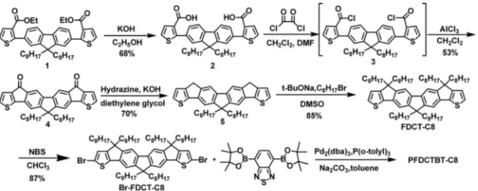
The synthesis of the key Br-FDCT-C8 monomer leading to PFDCTBT-C8 is shown in Scheme 1. Compound 1 with two ester groups was hydrolyzed to form compound 2 with two car-boxylic acids, which were then converted to acid chlorides by reacting with oxayl chloride to afford intermediate 3. Intra-molecular Friedel–Crafts acylation of 3 regioselectively occurred at the 3- and 6-positions of the central flourene to yield the hep-tacyclic arene 4. Wolff–Kishner reduction converted the two car-bonyl groups in compound 4 to the corresponding methylene
Chih-Yu Chang, Yen-Ju Cheng,* Shih-Hsiu Hung, Jhong-Sian Wu, Wei-Shun Kao,
Chia-Hao Lee, and Chain-Shu Hsu*
Combination of Molecular, Morphological, and Interfacial
Engineering to Achieve Highly Efficient and Stable Plastic
Solar Cells
C
OMMUNICA
TION
from the toluene solution to the solid state (Figure 2). Furthermore, the optical bandgap of PFDCTBT-C8 deduced from its absorp-tion edge in the solid state was determined to be 1.71 eV, which is narrower than that of PFDCTBT (1.76 eV). These optical behaviors confirm that the side chain modification of PFDCTBT-C8 effectively promotes stronger intermolecular interaction in the solid state.
The electrochemical properties of PFD-CTBT-C8 were estimated by cyclic voltam-metry (CV) (Figure S2). The flourene-based PFDCTBT-C8 showed a typical lower-lying HOMO level at –5.30 eV, which is an impor-tant criterion for obtaining high Voc in the resultant device.[3,4]
The lowest unoccupied molecular orbital (LUMO) level of PFDCTBT-C8 was determined to be –3.55 eV, that is, positioned 0.4 eV above that of electron acceptor PC71BM (–3.95 eV,
meas-ured under the same conditions), which will ensure energeti-cally favorable electron transfer.[3,4]
The field-effect hole mobilities of PFDCTBT and PFDCTBT-C8 were extracted from the transfer characteristics of the field-effect transistor (FET) devices fabricated with top-contact geo-metry using Au electrodes (Figure 3a). PFDCTBT-C8 exhibited a high field-effect hole mobility of 3.3 × 10⁻² cm2 V−1 s−1 owing
to the extended coplanarity and rigidity of FDCT’s structure. It should be noted that this value is higher than that of PFDCTBT (1.4 × 10⁻³ cm2 V−1 s−1) by an order of magnitude. This result
indicates that flexible aliphatic side chains in PFDCTBT-C8 strengthen the intermolecular π–π interaction to enhance the hole mobility compared to the ethylhexoxyphenyl side chains in PFDCTBT.
The solar cells with inverted architecture were fabricated based on the configuration indium tin oxide (ITO)/ZnO/C-PCBSD/ PFDCTBT-C8:PC71BM (1:3,
w/w)/poly(3,4-ethylenedioxythi-ophene) poly(styrenesulfonate) (PEDOT:PSS)/Ag where a cross-linked PC61BM derivative, [6,6]-phenyl-C61-butyric styryl dendron
ester (C-PCBSD), was used as an interlayer.[22–24] Current
den-sity–voltage (J–V) characteristics of the devices under AM1.5G solar irradiation with light intensity of 100 mW cm−2 are shown in Figure 3b, and the corresponding device parameters are sum-marized in Table 1. When the active layer was processed with only
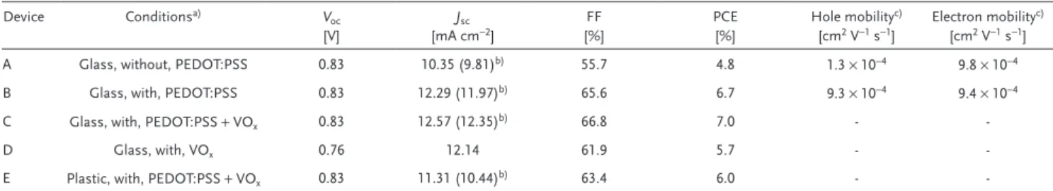
ortho-dichlorobenzene (ODCB) as the solvent, device A obtained
a high PCE of 4.8% with Voc of 0.83 V, Jsc of 10.35 mA cm−2, and
fill factor (FF) of 55.7% (Table 1 and Figure 3b). The nanometer-scale morphology of the active layer can be smartly controlled by judicial choice of the processing additives.[10,11,25]
Encourag-ingly, by adding 2.5 vol.% 1-chloronaphthalene (CN) into ODCB as the processing additive in device B, the PCE was dramatically improved to 6.7% as a result of the simultaneously increased
Jsc and FF values (Table 1 and Figure 3b). Note that the Jsc values
from J–V measurements are consistent with the values calcu-lated from integrated incident photon–to–current conversion efficiency (IPCE) spectra (Figure S3), which confirms the accu-racy of the reported PCE values.
To gain deep insight into the performance enhancement upon the introduction of CN additive, the morphological altera-tion of the blend films was investigated by atomic force micro-scopy (AFM) topography images (Figure S4). Compared to the groups in compound 5. Alkylation of compound 5 successfully
incorporated four octyl groups in FDCT-C8, which was then brominated by N-bromosuccinimide (NBS) to afford Br-FDCT-C8. This monomer was copolymerized with the 4,7-bis(4,4,5,5-tetramethyl-1,3,2-dioxaborolan-2-yl)-2,1,3-benzothiadiazole (BT) unit by Suzuki coupling to generate the D–A copolymer PFD-CTBT-C8, which showed a number-average molecular weight (Mn) of ca. 33 kDa with a polydispersity index of 2.87, as
deter-mined by gel permeation chromatography.
From thermal gravimetric analysis (TGA), we found PFD-CTBT-C8 had high thermal stability with a decomposition tem-perature (5% weight loss) of 437 °C (Figure S1, Supporting Information). The UV-vis absorption spectra of PFDCTBT-C8 in toluene showed two distinct absorption bands (Figure 2). The short-wavelength absorption band (ca. 417 nm) is assigned to a delocalized excitonic π–π* transition and the long- wavelength absorption band (ca. 621 nm) is ascribed to intramolecular charge transfer (ICT) interactions between the donor and acceptor moieties. It should be noted that the profiles of the absorption spectra of PFDCTBT are essentially the same in both the solution state and the solid state (Figure 2), indicating that the bulky 4-(2-ethylhexyloxy)phenyl moieties in PFD-CTBT dilute the interchain π–π interactions in the solid state. Nevertheless, the absorption maxima of PFDCTBT-C8, substi-tuted with flexible octyl side chains, red-shifted by ca. 20 nm
Scheme 1. Synthesis of Br-FDCT-C8 monomer and PFDCTBT-C8 copolymer.
Figure 2. UV–vis absorption spectra of PFDCTBT and PFDCTBT-C8 in toluene solution and in the film state.
C
OMMUNICA
TION
one order of magnitude (from 1.3 × 10⁻⁴ cm2 V−1 s−1 to 9.8 ×
10−4 cm2 V−1 s−1) while the electron mobilities of the devices
remained essentially unchanged (ca. 9.4 × 10⁻⁴ cm2 V−1 s−1).
In addition to the enhancement in SCLC hole mobility, the field-effect hole mobility of PFDCTBT-C8 was also increased from 3.3 × 10⁻² cm2 V−1 s−1 to 8.9 × 10⁻² cm2 V−1 s−1 by adding
2.5 vol% CN as the processing additive (Figure S6). In view of optimized morphology and enhanced hole mobility, we assume that the performance enhancement is attributed to the additive-assisted self-organization of PFDCTBT-C8 into a more favo-rable morphology that facilitates hole transporting properties. The more balanced electron/hole mobilities (the electron-to-hole mobility ratio is close to unity) can effectively reduce space charge build-up within the active layer.[9,27]
Based on the optimized molecular and morphological prop-erties, we envision that modulating interface characteristics between PEDOT:PSS layer and anode may play an impor-tant role in further improvement of inverted device perform-ance.[11,13] By inserting a solution-processed vanadium oxide
(VOx) film on top of the PEDOT:PSS layer in device C,[28,29] we
successfully achieved an exceptionally high PCE of 7%, which represents the highest value ever reported for fluorine-based bulk-heterojunction (BHJ) solar cells (Table 1, Figure 3b). Device C also exhibited a higher shunt resistance, of 5.8 MΩ cm2, than
device B, with 0.7 MΩ cm2 (Figure S7), indicating that the
leakage current in device B can be greatly suppressed by the VOx layer in device C. This result might be associated with the
passivation of the local shunts existing within the PEDOT:PSS layer.[30,31] However, device D, using VO
x as the single
hole-extraction layer (without PEDOT:PSS layer), exhibited a PCE reduced to 5.7%. This decrease obviously originated from the decreased Voc (Table 1 and Figure 3b). The mechanism of the Voc reduction in device D is not clear, but it may arise from
the poor electrical coherence at the organic/inorganic interface and/or trap formation as a result of the penetration of the vana-dium precursor into the active layer.[32–34] Further investigation
is currently under way in our laboratory.
In addition, the shelf-stability of devices B and C without encapsulation was evaluated by monitoring the evolution of their PCE as a function of time during storage under ambient condi-tions. (Figure 4a). In contrast to device B, which showed a more obvious decline, device C retained over 85% of its initial PCE after being exposed to ambient conditions for more than 690 h, suggesting that the VOx interlayer may act as a gas- permeation
barrier that prevents ambient H2O/O2 from degrading
the underlying organic materials.[35] PEDOT:PSS is known for
pristine film, the additive-processed PFDCTBT-C8:PC71BM film
showed more pronounced fiber-like nanostructures with greater surface roughness. To further understand the effect of the addi-tive on the device performance, electron- and hole-only devices were fabricated to estimate the charge mobilities of the blend films by a space charge limited current (SCLC) model;[26,27]
the results are shown in Table 1 and Figure S5. The additive-processed device exhibited a hole mobility increased by almost
Figure 3. a) Transfer characteristics (Vds = –60 V) of the FET devices
based on PFDCTBT and PFDCTBT-C8 thin films. b) Current density– voltage (J–V) characteristics of the as-fabricated solar cell devices A–E; see Table 1 for descriptions of the device types.
Table 1. Summary of the parameters based on the devices substrate/ITO/ZnO/C-PCBSD/PFDCTBT-C8:PC71BM (1:3, w/w)/HEL/Ag.
Device Conditionsa) Voc
[V]
Jsc
[mA cm−2] [%]FF PCE [%] Hole mobility
c)
[cm2 V−1 s−1] Electron mobility c) [cm2 V−1 s−1]
A Glass, without, PEDOT:PSS 0.83 10.35 (9.81)b) 55.7 4.8 1.3 × 10⁻⁴ 9.8 × 10⁻⁴
B Glass, with, PEDOT:PSS 0.83 12.29 (11.97)b) 65.6 6.7 9.3 × 10⁻⁴ 9.4 × 10⁻⁴
C Glass, with, PEDOT:PSS + VOx 0.83 12.57 (12.35)b) 66.8 7.0 -
-D Glass, with, VOx 0.76 12.14 61.9 5.7 -
-E Plastic, with, PEDOT:PSS + VOx 0.83 11.31 (10.44)b) 63.4 6.0 -
-a)Substrate, with or without CN additive, hole-extraction layer (HEL); b)Calculated from the IPCE spectra shown in Figure S3 (Supporting Information); c)Estimated by SCLC model.
C
OMMUNICA
TION
and lower optical transparency (Figure S8). Again, device E also exhibited excellent air stability, retaining over 80% of its initial PCE after being exposed to ambient conditions for more than 690 h (Figure 4a).
Device stability with respect to mechanical deformation is another important device parameter for flexible solar cells. To evaluate the mechanical stability under ambient conditions, planar device E was first bent to a circle with a radius of 12 mm followed by recovery to planar structure. After 1100 bending cycles in which an external force was consecutively applied and released, device E showed no significant decrease of efficiency, maintaining 87% of its original PCE (Figure 4b). This result demonstrated that device E possesses good flexibility without compromising its high device performance. The superior mechanical stability might be associated with the small thick-ness of the metal oxide layers (i.e., 20 nm ZnO and 15 nm VOx)
used in the device to avoid crack formation during the bending process.
In conclusion, by an acylation–reduction–alkylation strategy we have successfully synthesized a novel fluorine-based multi-fused D–A alternating copolymer PFDCTBT-C8 substituted with flexible octyl groups. PFDCTBT-C8 features a narrow bandgap of 1.71 eV, a low-lying HOMO level of –5.30 eV, and a high field-effect hole mobility of 3.3 × 10⁻² cm2 V−1 s−1.
Through engineering molecular structure to promote the inter-molecular interaction, using additive to assist the formation of the optimized morphology, and introducing a VOx interlayer
to improve the interfacial properties, we achieved a BHJ solar cell based on PFDCTBT-C8:PC71BM (1:3, w/w) blend with an
impressive PCE of 7%, which represents the highest value ever reported for fluorine-based BHJ solar cells. More significantly, the device constructed on the flexible PEN substrate not only achieved a record high PCE of 6% for plastic solar cells, but also exhibited exceptional air and mechanical stability.
Experimental Section
PSC Device Fabrication and Characterization: The device structure
of the solar cell device was substrate/ITO/ZnO/C-PCBSD/PFDCTBT-C8:PC71BM/PEDOT:PSS/with or without VOx/Ag. Substrates included
ITO-coated glass (purchased from Rite Displays; sheet resistance 15 Ω sq−1) and ITO-coated PEN (purchased from Perm Top Corp.; sheet
resistance 50 Ω sq−1). The device fabrication procedure was described as
follows: 1) spin casting of the ZnO precursor from zinc acetylacetonate hydrate (purchased from Aldrich and used as received) dissolved in methanol (20 mg mL−1) onto the pre-cleaned ITO surface and subsequent baking at 130 °C for 10 min in air (20 nm); 2) spin casting of PCBSD solution (7 mg mL−1 in ODCB) on top of the ZnO layer (ca.
10 nm) and subsequent baking at 150 °C for 10 min; 3) spin casting of the active layer (150 nm) from an ODCB solution of PFDCTBT-C8 (6 mg mL−1) and PC
71BM (18 mg mL−1, purchased from Solenne and
used as received); 4) spin casting of the PEDOT:PSS layer (Clevios P from Heraeus Clevios) diluted with an equal volume of 2-propanol and 0.2 wt% polyoxyethylene-6-tridecylether (Aldrich) followed by baking at 60 °C for 10 min (60 nm); 5) spin casting of the VOx layer (15 nm) from
the isopropyl alcohol solution of vanadium(V) triisopropoxy (purchased from Alfa Aesar and used as received) at 1:70 volume ratio for the device containing the VOx layer;[28] 6) thermal evaporation of the Ag layer
under high vacuum (<10−6 Torr; 200 nm) through a shadow mask that
defined an active area of 0.04 cm2; 7) thermal annealing of the complete
device at 150 °C for 5 min. The J–V characteristics of the PSC devices
its acidity, which could result in erosion or passivation of the adjacent electrode. Avoiding direct contact between PEDOT:PSS and the Ag electrode by inserting a VOx interlayer might also
be a possible reason for the improved long-term stability. To truly exploit flexibility of PSCs for practical use, multi-layer devices have to be integrated with a plastic substrate. However, plastic-based solar cells still suffer from insufficient efficiency and poor stability compared to their glass-based counterparts.[5] So far, the realization of plastic solar cells with
PCE values above 5% has not been successful.[36] It is highly
desirable to transfer our optimal device configuration from a glass substrate to a plastic substrate. By taking advantage of the fact that all the device fabrication processing conditions in this research were at low temperatures below 150 °C, we suc-cessfully fabricated device E on ITO-coated poly(ethylene naph-thalate) (PEN) substrate. As shown in Table 1 and Figure 3b, device E exhibited an exceptional PCE of 6%, with Voc of 0.83 V, Jsc of 11.31 mA cm−2, and FF of 63.4%. The lower efficiency
observed in device E relative to device C is due to intrinsic limi-tations of the PEN plastic substrate, including the higher ITO sheet resistance (50 Ω sq−1 vs. 15 Ω sq−1 on the glass substrate) Figure 4. a) Degradation profiles of the unencapsulated devices B, C, and E stored at 30 °C in ambient air. b) The PCE degradation profile of flexible device E during consecutive bending cycles with a radius of 12 mm.
C
OMMUNICA
TION
were measured with a Keithley 2400 source meter under simulated AM1.5G illumination (SAN-EI XES-301S solar simulator with integrated intensity of 100 mW cm−2), which was calibrated with a Hamamatsu
silicon photodiode with KG-5 filter against an NREL-calibrated solar simulator.[37] IPCE spectra were measured using a lock-in amplifier with
a current preamplifier under short-circuit conditions with illumination by monochromatic light from a 250 W quartz-halogen lamp (Osram) passing through a monochromator (Spectral Products CM110).
FET Device Fabrication and Characterization: Top-contact, bottom-gate
FET devices were fabricated on heavily doped n-type Si wafer substrates with thermally grown SiO2 gate dielectric (300 nm, capacitance
10 nF cm−2).[38] The cleaned substrates were immersed in a 0.1 m solution
of octadecyltrichlorosilane (OTS) in toluene at 60 °C for 3 h under an inert atmosphere followed by rinsing with toluene and then drying with N2. The PFDCTBT and PFDCTBT-C8 solutions (7 mg mL−1 in ODCB)
were then deposited on top of the OTS-modified SiO2 surface followed by
baking at 150 °C for 5 min. Subsequently, the Au source/drain electrodes were deposited by thermal evaporation through a shadow mask to finish the FET devices with channel length L and channel width W of 60 μm and 3500 μm, respectively. Electrical characterization was carried out under vacuum using an Agilent 4156C semiconductor parameter analyzer. The FET mobility was extracted from the following equation in the saturation regime: ID = μCi (W/2L)(VG−VT)2,[38] where ID is the drain current, W and
L are the channel width and length, respectively, Ci is the capacitance per
unit area of the gate dielectric, and VG is the gate voltage.
Supporting Information
Supporting Information is available from the Wiley Online Library or from the author.
Acknowledgements
This work is supported by the National Science Council and “ATP Plan” of the National Chiao Tung University and Ministry of Education, Taiwan.
Received: October 13, 2011 Published online: December 20, 2011
[10] J. Peet, J. Y. Kim, N. E. Coates, W. L. Ma, D. Moses, A. J. Heeger, G. C. Bazan, Nat. Mater. 2007, 6, 497.
[11] L. M. Chen, Z. Hong, G. Li, Y. Yang, Adv. Mater. 2009, 21, 1434. [12] M. D. Irwin, D. B. Buchholz, A. W. Hains, R. P. H. Chang, T. J. Marks,
Proc. Natl. Acad. Sci. USA 2008, 105, 2783.
[13] H. Ma, H.-L. Yip, F. Huang, A. K. Y. Jen, Adv. Funct. Mater. 2010, 20, 1371.
[14] F. Zhang, W. Mammo, L. M. Andersson, S. Admassie, M. R. Andersson, O. Inganäs, Adv. Mater. 2006, 18, 2169.
[15] M. H. Chen, J. Hou, Z. Hong, G. Yang, S. Sista, L. M. Chen, Y. Yang,
Adv. Mater. 2009, 21, 4238.
[16] W. Wu, Y. Liu, D. Zhu, Chem. Soc. Rev. 2010, 39, 1489.
[17] M. Forster, K. O. Annan, U. Scherf, Macromolecules 1999, 32, 3159. [18] M. Forster, J. Y. Pan, K. O. Annan, D. Haarer, U. Scherf, Polym. Int.
2000, 49, 913.
[19] J. S. Wu, Y. J. Cheng, M. Dubosc, C. H. Hsieh, C. Y. Chang, C. S. Hsu,
Chem. Commun. 2010, 46, 3259.
[20] M. Zhang, X. Guo, X. Wang, H. Wang, Y. Li, Chem. Mater. 2011, 23, 4264.
[21] Y. J. Cheng, J. S. Wu, P. I. Shih, C. Y. Chang, P. C. Jwo, W. S. Kao, C. S. Hsu, Chem. Mater. 2011, 23, 2361.
[22] C. H. Hsieh, Y. J. Cheng, P. J. Li, C. H. Chen, M. Dubosc, R. M. Liang, C. S. Hsu, J. Am. Chem. Soc. 2010, 132, 4887.
[23] Y.-J. Cheng, C.-H. Hsieh, Y. He, C.-S. Hsu, Y. Li, J. Am. Chem. Soc. 2010, 132, 17381.
[24] C.-Y. Chang, C.-E. Wu, S.-Y. Chen, C. Cui, Y.-J. Cheng, C.-S. Hsu, Y.-L. Wang, Y. Li, Angew. Chem. Int. Ed. 2011, 50, 9386.
[25] C. V. Hoven, X. D. Dang, R. C. Coffin, J. Peet, T. Q. Nguyen, G. C. Bazan, Adv. Mater. 2010, 22, E63.
[26] M. F. Falzon, M. M. Wienk, R. A. J. Janssen, J. Phys. Chem. C 2011,
115, 3178.
[27] V. D. Mihailetchi, H. Xie, B. De Boer, L. J. A. Koster, P. W. M. Blom,
Adv. Funct. Mater. 2006, 16, 699.
[28] K. Zilberberg, S. Trost, H. Schmidt, T. Riedl, Adv. Energy Mater. 2011,
1, 377.
[29] C. P. Chen, Y. D. Chen, S. C. Chuang, Adv. Mater. 2011, 23, 3859. [30] A. W. Hains, T. J. Marks, Appl. Phys. Lett. 2008, 92, 0235041. [31] M. Kemerink, S. Timpanaro, M. M. de Kok, E. A. Meulenkamp,
F. J. Touwslager, J. Phys. Chem. B 2004, 108, 18820.
[32] C. Goh, S. R. Scully, M. D. McGehee, J. Appl. Phys. 2007, 101, 114503.
[33] K. Zilberberg, S. Trost, J. Meyer, A. Kahn, A. Behrendt, D. Lützenkirchen-Hecht, R. Frahm, T. Riedl, Adv. Funct. Mater. doi: 10.1002/adfm.201101402.
[34] S. R. Cowan, W. L. Leong, N. Banerji, G. Dennler, A. J. Heeger, Adv.
Funct. Mater. 2011, 21, 3083.
[35] H. Hintz, H. J. Egelhaaf, L. Lüer, J. Hauch, H. Peisert, T. Chassé,
Chem. Mater. 2011, 23, 145.
[36] J.-C. Wang, W.-T. Weng, M.-Y. Tsai, M.-K. Lee, S.-F. Horng, T.-P. Perng, C.-C. Kei, C.-C. Yu, H.-F. Meng, J. Mater. Chem. 2010, 20, 862. [37] V. Shrotriya, G. Li, Y. Yao, T. Moriarty, K. Emery, Y. Yang, Adv. Funct.
Mater. 2006, 16, 2016.
[38] J. H. Oh, H. W. Lee, S. Mannsfeld, R. M. Stoltenberg, E. Jung, Y. W. Jin, J. M. Kim, J. B. Yoo, Z. Bao, Proc. Natl. Acad. Sci. USA 2009, 106, 6065.
[1] M. Pagliaro, R. Ciriminna, G. Palmisano, ChemSusChem 2008, 1, 880.
[2] G. Yu, J. Gao, J. C. Hummelen, F. Wudl, A. J. Heeger, Science 1995,
270, 1789.
[3] K. M. Coakley, M. D. McGehee, Chem. Mater. 2004, 16, 4533. [4] B. C. Thompson, J. M. J. Fréchet, Angew. Chem. Int. Ed. 2008, 47, 58. [5] C. J. Brabec, S. Gowrisanker, J. J. M. Halls, D. Laird, S. Jia,
S. P. Williams, Adv. Mater. 2010, 22, 3839. [6] Y. Li, Y. Zou, Adv. Mater. 2008, 20, 2952.
[7] Y. J. Cheng, S. H. Yang, C. S. Hsu, Chem. Rev. 2009, 109, 5868. [8] C. A. Junwu, C. Yong, Acc. Chem. Res. 2009, 42, 1709.
[9] G. Li, V. Shrotriya, J. Huang, Y. Yao, T. Moriarty, K. Emery, Y. Yang,