IEEE ELECTRON DEVICE LETTERS, VOL. 29, NO. 2, FEBRUARY 2008 165
Analysis of Negative Bias Temperature Instability
in Body-Tied Low-Temperature Polycrystalline
Silicon Thin-Film Transistors
Chih-Yang Chen, Student Member, IEEE, Ming-Wen Ma, Wei-Cheng Chen, Hsiao-Yi Lin,
Kuan-Lin Yeh, Shen-De Wang, and Tan-Fu Lei
Abstract—Negative bias temperature instability (NBTI)
degra-dation mechanism in body-tied low-temperature polycrystalline silicon thin-film transistors (LTPS TFTs) is analyzed by the charge-pumping (CP) technique. The properties of bulk trap states (includ-ing interface and grain boundary trap states) are directly charac-terized from the CP current. The increase of the fixed oxide charges is also extracted, which has not been quantified in previous stud-ies of NBTI degradation in LTPS TFTs. The experimental results confirm that the NBTI degradation in LTPS TFTs is caused by the generation of bulk trap states and oxide trap states.
Index Terms—Charge-pumping (CP) technique,
low-temperature polycrystalline silicon thin-film transistors (LTPS TFTs), negative bias temperature instability (NBTI).
I. INTRODUCTION
L
OW-TEMPERATURE polycrystalline silicon thin-film transistors (LTPS TFTs) are attracting much research in-terest as potential candidates for the realization of system on panel (SOP). For driving circuit operation, LTPS TFTs must be designed using the CMOS inverter configuration. During op-eration, p-channel TFT will be subjected to negative bias tem-perature instability (NBTI) when the input is at a low voltage level and the output is at a high voltage level. In MOSFETs, it is well accepted that the NBTI degradation originates from the breaking of the hydrogenated silicon (Si–H) bonds, resulting in the generation of interface and oxide trap states [1]–[3]. How-ever, in LTPS TFTs, due to the existence of trap states in the grain boundaries and at the poly-Si/SiO2 interface, more Si–H bonds may be found in the channel region than with MOSFETs. Further, due to the poor thermal conductivity of the glass sub-strate and high operating voltage, NBTI can be an important reliability issue for LTPS TFTs. Therefore, it is important to study NBTI behaviors and the related degradation mechanisms of LTPS TFTs.Manuscript received September 14, 2007; revised November 9, 2007. This work was supported by the National Science Council, Taiwan, R.O.C., under Contract NSC95-2221-E-009-279. The review of this letter was arranged by Editor J. Sin.
C.-Y. Chen, M.-W. Ma, S.-D. Wang, and T.-F. Lei are with the Institute of Electronics, National Chiao Tung University, Hsin-Chu 300, Taiwan, R.O.C. (e-mail: [email protected]; [email protected]; bryant519@ yahoo.com.tw; [email protected]).
W.-C. Chen, H.-Y. Lin, and K.-L. Yeh are with the Toppoly Optoelectronics Corporation, Chu-Nan 350, Taiwan, R.O.C. (e-mail: [email protected]; [email protected]; [email protected]).
Color versions of one or more of the figures in this letter are available online at http://ieeexplore.ieee.org.
Digital Object Identifier 10.1109/LED.2007.914083
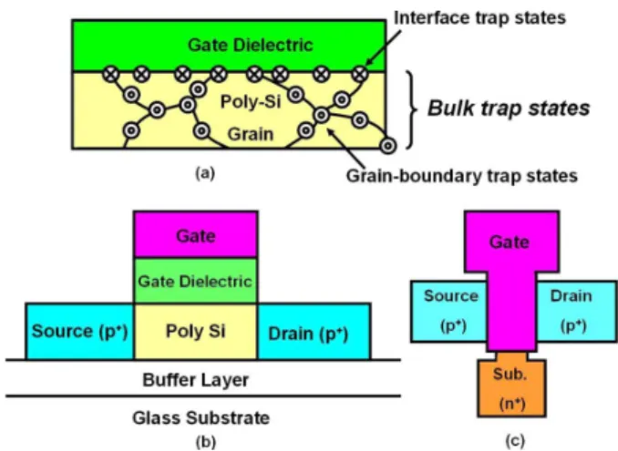
Fig. 1. (a) Schematic cross-sectional view of the critical poly-Si/SiO2
inter-face showing interinter-face trap states and grain boundary trap states. (b) Cross-sectional and (c) top views of the LTPS TFT used in this letter.
NBTI has been reported to degrade the channel film of LTPS TFTs [4]. In previous studies, the channel properties have been found to be derived from the current–voltage characteristics. However, the channel current is affected through the potential barrier formed by the trap states [5]. Therefore, the bulk trap-state density (Nbulk) derived from the channel current does not indicate the real bulk trap-state density, but the effective bulk trap-state density. Koyanagi and coworkers [6], [7] and Bal-asinski and coworkers [8]–[10] proposed the charge-pumping (CP) technique to directly characterize the bulk trap properties of poly-Si TFTs. Unlike in MOSFETs, in LTPS TFTs, the grain boundary trap states also give rise to the CP current (IC P). Con-sequently, Nbulk as measured by the CP technique consists of both the grain boundary and interface trap states, as shown in Fig. 1(a). Nbulk can be revealed from IC Pbecause carriers are observed as the generation–recombination current. As a result, the influence of Nbulk is directly evaluated. However, use of this technique to analyze the NBTI effect in LTPS TFTs has not been reported. Given this, the aim of our study is to use the CP technique to investigate the behavior of Nbulk during NBTI stress. Further, the role of oxide trap-state generation in the NBTI degradation mechanism is also identified.
II. EXPERIMENT
P-channel LTPS TFTs (W/L = 10 µm/10 µm) were fabri-cated on glass substrates. A 40-nm-thick amorphous Si layer was deposited by plasma enhanced chemical vapor deposition
166 IEEE ELECTRON DEVICE LETTERS, VOL. 29, NO. 2, FEBRUARY 2008
Fig. 2. Transfer characteristics of the LTPS TFT before and after 1000 s NBTI stress at 150◦C with the stress voltage of−20 V.
(PECVD) on a buffer layer and crystallized into poly-Si film by excimer laser annealing. Ion implantation was performed on the extra body terminal to form the heavily doped n+ region. A 100-nm-thick SiO2 layer was deposited as the gate dielec-tric followed by Mo deposition as the gate. After source/drain formation, hydrogenation was performed with NH3 treatment. Then, the interlayer dielectric was deposited and densified, and the dopants were activated during this step. Finally, intercon-nection metal was deposited and patterned. The schematic cross sectional and top views of the device are shown in Fig. 1(b) and 1(c), respectively.
The NBTI stress was performed at the temperature ranging from 75◦C to 150◦C, and a gate voltage in the range of−13 to
−20 V was applied with the source, drain, and body grounded.
During the CP measurement, a pulse train with frequency of 100 kHz and fixed pulse amplitude of 1.5 V were applied to the gate while IC P was measured between the source/drain and
substrate contact, and the base voltage was varied to tune the surface condition from inversion to accumulation.
III. RESULTS ANDDISCUSSION
Fig. 2 shows the transfer characteristics of the LTPS TFT be-fore and after the NBTI stress. The device shows degradation in the subthreshold swing and field-effect mobility, indicating that interface trap states were generated [11]. Further, the threshold voltage (Vth) shifts to the negative direction after the stress. Degradation can be attributed to the generation of bulk trap states and oxide trap states. Detailed analysis of these trap-state generations will be discussed later.
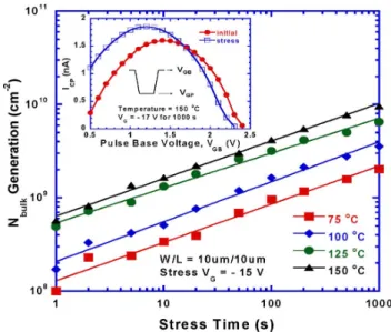
The inset of Fig. 3 shows the IC P of the device before and after 1000 s NBTI stress. The increase in IC P indicates that bulk trap states are generated during NBTI stress. Further, the
IC P curve shifts to the negative direction, implying that a net positive charge is clearly generated in the oxide or/and at the interface. Fig. 3 shows the time dependence of the Nbulk gener-ation (∆Nbulk), which is calculated from IC P. ∆Nbulkfollows a power law dependence on the stress time with an exponent factor of 0.37–0.42, implying that diffusion-controlled electro-chemical reactions may take part in the process [12], [13].
Fig. 3. Time dependence of the bulk trap-state density generation under var-ious stress conditions. The inset shows the IC Pbefore and after 1000 s NBTI
stress.
Fig. 4. Dependences of bulk trap-state density generation on the (a) stress voltage and (b) stress temperature of the LTPS TFTs under various stress conditions.
Further, ∆Nbulkalso exhibits an exponential dependence on the stress voltage (VG) and the reciprocal of temperature (1/T).
The experimental results show that the Nbulk variation can be expressed as
∆Nbulk ∝ tne(−Ea/k T )eC|VG|. (1)
The parameter C extracted from Fig. 4(a) is between 0.14 and 0.19, which is dependent on the process [14]. The activation en-ergy (Ea) extracted from Fig. 4(b) is between 0.25 and 0.30 eV.
∆Nbulkincreases with the stress voltage or temperature, imply-ing that Nbulk generation can be electrically and thermally ac-tivated. On the other hand, the charge-trapping model is unable
CHEN et al.: ANALYSIS OF NBTI IN BODY-TIED LOW-TEMPERATURE POLYCRYSTALLINE Si TFTs 167
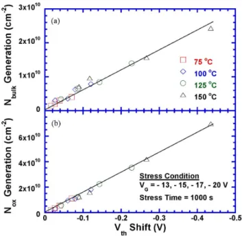
Fig. 5. Correlation between the increases of the (a) bulk trap-state density, (b) oxide trap-state density, and the threshold voltage shift.
to explain the exponential dependence of the Vth shift (∆Vth) on VG and 1/T [15], [16]. Furthermore, the electric field across
the gate dielectric (below 2 MV/cm) was not high enough to cause hole injection. Therefore, we thus provide further confir-mation that the NBTI degradation in LTPS TFTs is attributable to diffusion-controlled electrochemical reactions instead of the charge-trapping model.
Fig. 5(a) presents the correlation between ∆Nbulkand ∆Vth, in which both these two physical quantities show a linear correla-tion. Because the degradation can be explained by the diffusion-controlled electrochemical reactions [12], [13], we can assume the ∆Vth is caused by the generation of Nbulk and oxide trap-state density (Nox). Therefore, the threshold voltage shift (∆Vth) may simply expressed as
∆Vth =−
q(∆Nbulk+ ∆Nox)
Cox
. (2)
According to (2), ∆Noxcan be calculated from the measured ∆Vth and ∆Nbulk. Fig. 5(b) shows the correlation between ∆Nox and ∆Vth. We can conclude that ∆Nbulk alone cannot explain the measured ∆Vth and that ∆Nox must be taken into account.
By expanding the model proposed for bulk-Si MOSFETs [17], we introduce a model to explain the NBTI degradation mechanism for LTPS TFTs. The Si dangling bonds in the bulk channel region are assumed to be initially passivated by hydro-gen atoms. During NBTI stress, the hydrohydro-gen atoms react with the holes and dissociate from the Si atoms, resulting in the gen-eration of bulk trap states. The released hydrogen species diffuse or drift into the gate oxide and react with it, forming OH groups bounded to oxide Si atoms and leaving positive oxide trap states in the gate oxide. Finally, the hydrogen species diffuse into the gate oxide, becoming the reaction-limiting factor.
IV. CONCLUSION
For the first time, the CP technique is utilized to analyze the NBTI degradation mechanism in LTPS TFTs. The properties of
Nbulk can be directly characterized from IC P. In addition, the increase of Nox is also extracted. Our results show that both ∆Nbulk and ∆Nox are closely related to ∆Vth. This further confirms that ∆Nbulkalone cannot explain the measured ∆Vth and that ∆Nox must be taken into account. On the other hand, experimental results show that NBTI degradation can be electri-cally and thermally activated. Therefore, the operating voltage and power consumption have to be carefully designed, and new processes must be developed to suppress NBTI degradation and realize SOP.
REFERENCES
[1] C. E. Blat, E. H. Nicollian, and E. H. Poindexter, “Mechanism of negative-bias-temperature instability,” J. Appl. Phys., vol. 63, pp. 1712–1720, 1991.
[2] D. K. Schroder and J. A. Babcock, “Negative bias temperature instability: Road to cross in deep submicron silicon semiconductor manufacturing,”
J. Appl. Phys., vol. 94, pp. 1–18, 2003.
[3] A. Scarpa, D. Ward, J. Dubois, L. V. Marwijk, S. Gausepohl, R. Campos, K. Y. Sim, A. Cacciato, R. Kho, and M. Bolt, “Negative-bias temperature instability cure by process optimization,” IEEE Trans. Electron Devices, vol. 53, no. 6, pp. 1331–1339, Jun. 2006.
[4] S. Maeda, S. Maegawa, T. Ipposhi, H. Nishimura, T. Ichiki, J. Mitsuhashi, M. Ashida, T. Muragishi, and T. Nishimura, “Negative bias temperature instability in poly-Si TFTs,” in VLSI Symp. Tech. Dig., 1993, pp. 29–30. [5] L. Levinson, F. R. Shephred, P. J. Scanlon, W. D. Westwood, G. Este, and
M. Rider, “Conductivity behavior in polycrystalline semiconductor thin film transistors,” J. Appl. Phys., vol. 53, pp. 1193–1202, 1982. [6] M. Koyanagi, I.-W. Wu, A. G. Lewis, M. Fuse, and R. Bruce, “Evaluation
of polycrystalline silicon thin film transistors with the charge-pumping technique,” in IEDM Tech. Dig., 1990, pp. 34.6.1–34.6.4.
[7] M. Koyanagi, Y. Baba, K. Hata, I.-W. Wu, A. G. Lewis, M. Fuse, and R. Bruce, “The charge-pumping technique for grain boundary trap eval-uation in polysilicon TFT’s,” IEEE Electron Device Lett., vol. 13, no. 3, pp. 152–154, Mar. 1992.
[8] A. Balasinski, J. Worley, M. Zamanian, and F. T. Liou, “Reference voltages and their stress-induced changes in thin film transistors as determined by charge pumping,” in IEDM Tech. Dig., 1995, pp. 529–532.
[9] A. Balasinski, J. Worley, K. W. Huang, J. Walters, and F. T. Liou, “Ob-servation of two types of trapping centers in thin film transistors using charge pumping technique,” IEEE Electron Device Lett., vol. 16, no. 10, pp. 460–462, Oct. 1995.
[10] A. Balasinski, J. Worley, K. W. Huang, and F. T. Liou, “Identification of Si/SiO2interface properties in thin film transistors with charge pumping
technique,” J. Electrochem. Soc., vol. 142, pp. 2717–2721, 1995. [11] T.-J. King, M. G. Hack, and I.-W. Wu, “Effective density-of-states
distri-butions for accurate modeling of polycrystalline-silicon thin-film transis-tors,” J. Appl. Phys., vol. 75, pp. 908–913, 1994.
[12] S. Ogawa and N. Shiono, “Generalized diffusion-reaction model for the low-field charge-buildup instability at the Si-SiO2interface,” Phys. Rev.
B, vol. 51, pp. 4218–4230, 1995.
[13] S. Ogawa, M. Shimaya, and N. Shiono, “Interface-trap generation at ultra-thin SiO2(4–6 nm)-Si interfaces during negative-bias temperature aging,”
J. Appl. Phys., vol. 77, pp. 1137–1148, 1995.
[14] A. T. Krishnan, V. Reddy, and S. Krishnan, “Impact of charging damage on negative bias temperature instability,” in IEDM Tech. Dig., 2001, pp. 865– 868.
[15] M. J. Powell, C. V. Berkel, and J. R. Hughes, “Time and temperature de-pendence of instability mechanisms in amorphous silicon thin-film tran-sistors,” Appl. Phys. Lett., vol. 54, pp. 1323–1325, 1989.
[16] N. D. Young and A. Gill, “Electron trapping instabilities in polycrystalline silicon thin film transistor,” Semicond. Sci. Technol., vol. 5, pp. 72–77, 1990.
[17] K. O. Jeppson and C. M. Svensson, “Negative bias stress of MOS devices at high electric fields and degradation of MNOS devices,” J. Appl. Phys., vol. 48, pp. 2004–2014, 1977.