IEEE TRANSACTIONS ON DEVICE AND MATERIALS RELIABILITY, VOL. 9, NO. 1, MARCH 2009 59
Board-Level ESD of Driver ICs on LCD Panel
Jen-Chou Tseng, Chung-Ti Hsu, Chia-Ku Tsai, Shu-Chuan Chen, and Ming-Dou Ker, Fellow, IEEE
Abstract—In this paper, a method utilizing a charged-device model (CDM) test by the tape carrier package or chip-on-film (COF) samples to emulate the real-world board-level CDM or charged-board model (CBM) electrostatic discharge is proposed for large-sized chips such as liquid-crystal display (LCD) driver ICs, which successfully duplicated the same failure by CBM dis-charging. For small-sized chips, the evaluation board (or printed circuit board) emulation should minimize the parasitic RLC loading of the interconnection on the board to achieve a more accu-rate CBM discharging. In addition, guidelines regarding chip-level design and layout optimization are proposed and have been suc-cessfully implemented to improve the immunity.
Index Terms—Charged-board model (CBM), electrostatic discharge (ESD).
I. INTRODUCTION
I
NTEGRATED circuits (ICs) surviving component-level electrostatic discharge (ESD) test may be prone to damage by a board-level device model (CDM) or charged-board model (CBM) stress, depending on the printed circuit board (PCB) design, board capacitance, and the environmental control of ESD [1]–[12]. The PCB and ICs on the board can accumulate electrostatic charges during manufacturing steps. Also, the larger the capacitance, the more charges can be induced and coupled. Once the power supply is plugged into the PCB, or the subsequent grounding process takes place, these accumulated charges can instantaneously discharge through the ICs and cause permanent damage. According to previous studies, the waveform of CBM discharge has a much higher peak current and a faster rise time than that of the human-body model (HBM), machine model (MM), and CDM for a given charge voltage. It is due to the lower inductance and resistance of the discharge path and the much larger effective capacitance of a board in comparison with the IC package. Thus, CBM damage is more severe than that in the other ESD models.To duplicate the CBM failure in laboratory, Olney et al. [10] were the first to propose a testing methodology for CBM using a field-induced CDM (FICDM) tester. CBM simulations were performed by the evaluation and production boards for dual operational amplifier and digital signal processing ICs, respectively. The evaluation board was made by the flame retardant 4 (FR4) dielectric material sandwiched in-between Manuscript received August 7, 2007; revised December 14, 2007. Current version published March 6, 2009.
J.-C. Tseng and C.-K. Tsai are with Taiwan Semiconductor Manufacturing Company, Hsinchu 300, Taiwan (e-mail: jctseng1@gmail.com).
C.-T. Hsu and S.-C. Chen are with Nuvoton Technology Corporation, Hsinchu 300, Taiwan (e-mail: tommy_alfa@yahoo.com.tw).
M.-D. Ker is with the Institute of Electronics, National Chiao Tung Univer-sity, Hsinchu 300, Taiwan (e-mail: mdker@ieee.org).
Color versions of one or more of the figures in this paper are available online at http://ieeexplore.ieee.org.
Digital Object Identifier 10.1109/TDMR.2008.2009931
two thick copper planes, and a decapsulated IC was soldered at the center of the top plane. The production board was cut down from the real PCB to fit the size of the charge board of the commercial FICDM tester. The decapsulated IC was located near the original corner of the PCB. Due to the large parasitic capacitance of the boards, the CBM events were therefore simulated by the large amount of induced charges, and the CBM failures were successfully replicated.
In this paper, a series of systematic investigations of CBM ESD damages have been performed to enhance the CBM im-munity of source/gate driver ICs attached to the printed wiring films, tape carrier package (TCP), or chip on film (COF) on the liquid-crystal display (LCD). To look for the ICs’ weakest point, PCB CDM tests similar to the proposal of Olney et al. [10] and the TCP/COF CDM test were performed to emulate CBM ESD events. The major difference between these two approaches is that the parasitic capacitance of TCP/COF is much smaller than that of PCB. However, the results showed that both approaches can result in the same damages. Finally, according to the failure analysis results and the follow-up layout optimization, the chip-level CBM ESD immunity was greatly improved, and the defect parts per million (DPPM) was enormously reduced. Guidelines regarding ESD cell design and layout optimization are also proposed.
II. EXPERIMENTS
One LCD source driver IC (TCS0001) and two LCD gate driver ICs (TCG0001 and TCG0002) were used for the fol-lowing experiments. The ICs were attached to TCP or COF and mounted on the high-capacitance PCB evaluation board, as shown in Fig. 1(a). The PCB is a four-layer FR4 multilayer construction, as shown in Fig. 1(b), which is very similar to the proposal of Olney et al. [10]. The top side is used for the bond-pad connection between the PCB and TCP or COF samples. Some bonding options are designed to study the effects of a resistor in series and a capacitor in parallel with the bond pads such as power, input, and output, as shown in Fig. 1(c). The bottom side, ground plane, is covered by paint to isolate from the charging plate of the CDM tester. The chip sizes of TCS0001, TCG0001, and TCG0002 were 12000µm × 1600µm, 6500 µm × 1400 µm, and 6500 µm × 1400 µm, and the parasitic capacitances were about 300, 700, and 700 pF, respectively. The parasitic capacitance was measured between the IC pad and the JEDEC-standard CDM charging plate by an HP4284 LCR meter at high frequency (1 MHz). The CDM testing was done on the commercial ThermoKeyTek ZapMaster 7/4 with maximum CDM±2000-V discharging, and the I–V characteristic was measured by an HP4155 precision meter. The discharging waveforms were measured by a Tektronix 1530-4388/$25.00 © 2009 IEEE
Fig. 1. (a) IC was attached to TCP or COF and mounted on the high-capacitance PCB evaluation board. (b) PCB is a four-layer FR4 multilayer construction. (c) Some bonding options are designed to study the effects of a resistor in series and a capacitor in parallel. (d) PCB evaluation board was put on the charging plate to perform the CDM test.
TCP312/TCPA300 current probe and a TDS7104 oscilloscope with 1-GHz bandwidth. Two emulations to duplicate the CBM failure and evaluate the CBM immunity are presented as fol-lows. The procedure was repeated with a 200- or 250-V-voltage step until the IC failed due to pin orVSUPPLYleakages.
1) PCB CDM Test: The following descriptions are the test
methods.
1) Measure theI–V characteristics of parasitic pull-up/pull-down diodes of the pin under test (PUT), as well as
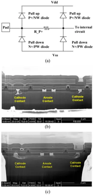
Fig. 2. (a) Circuit schematic diagram of the output pin of TCS0001. SEM photographs of the pull-up diodes of (b) the rejected product and (b) after the PCB CDM+1000-V test. The same contact spiking at the cathode was successfully duplicated by PCB emulation.
the leakage current betweenVSUPPLYand ground(VSS) before the CDM test.
2) Put the PCB on the charging plate and perform the CDM test, as shown in Fig. 1(d).
3) Check theI–V characteristics of the PUT and the leakage current betweenVSUPPLYandVSSafter the CDM test.
2) TCP/COF CDM Test: To simplify the process described
in the PCB CDM test, the TCP/COF CDM test is proposed to duplicate the CBM ESD failures. The evaluated PCB’s fabrication can be omitted, and the verification processes such as the function test after CDM stress become more easy because the steps of attaching and removing the TCP/COF samples from PCBs are already eliminated. The test methods are as follows.
1) Measure the I–V characteristics of the PUT and the leakage current between VSUPPLY and VSS before the
TSENG et al.: BOARD-LEVEL ESD OF DRIVER ICs ON LCD PANEL 61
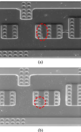
Fig. 3. (a) Circuit schematic diagram of the LV input pin of TCG0001. SEM photographs of the failed sites of PCB emulations (a)+800-V and (b) −600-V discharging.
CDM test without mounting the TCP/COF sample on the PCB.
2) Put the TCP/COF sample on the charging plate, and perform the CDM test for the PUT.
3) Check theI–V characteristics of the PUT and the leakage current betweenVSUPPLYandVSSafter the CDM test.
III. RESULTS ANDDISCUSSIONS
A. CBM Damages Duplicated by PCB Emulation
TCS0001 is fabricated by a 0.6-µm 10-V complementary-metal–oxide–semiconductor (CMOS) process. It is a source driver IC for LCD panel application that is packaged by TCP and passed the HBM 4-kV, MM 200-V, CDM ±500-V, and latch-up ±200-mA test criteria. However, the rejected
Fig. 4. SEM photographs of the failed sites of COF emulations (a)+1000-V and (b)−1000-V discharging, which are the same as that by PCB emulation. ICs showed that the output pin’s pull-up (pad-to-VSUPPLY) ESD protection diode was destroyed after the module assem-bly process. To verify the ESD-like damage, the CDM test method described in the aforementioned PCB emulation was performed. The results revealed that the output pin’s pull-up ESD protection diode was damaged after CDM +1000- and
−1500-V tests. According to the failure analysis results, both I–V measurement and scanning-electron-microscope (SEM)
cross-sectional photographs showed the same symptoms as that of the rejected ICs. Therefore, the root cause is considered to be the CBM ESD damage. Fig. 2 shows the circuit schematic diagram and the SEM cross-sectional photographs. The weak point of the diode is due to the nonuniform electric field and insufficient ballast resistance between the anode and the cathode.
B. Correlation Between PCB and TCP/COF Emulations
TCG0001 is fabricated by a 0.6-µm 40-V CMOS process and passed the HBM 2-kV, MM 200-V, CDM±500-V, and latch-up
±100-mA test criteria. It is the gate driver IC for LCD panel
application that is packaged by COF. The low-voltage (LV) input pin was tested by PCB emulation and failed the CDM +800-V/−600-V test. Failure analysis found damages at input gate oxide and parasitic n-p-n bipolar-junction transistor in the internal circuit. Fig. 3 shows the circuit schematic diagram and the SEM top-view photographs of the failed LV input pin. As can be seen, the input p-channel MOS field-effect transistors
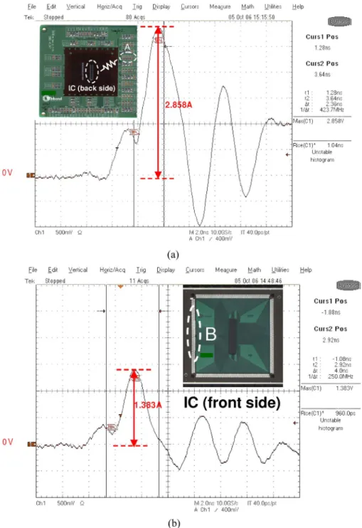
Fig. 5. Waveforms measured from the (a) golden pad (point A) on the PCB evaluation board and (b) I/O pad (point B) on COF under 100-V discharging. The peak voltage of discharging measured on A was about two times that on B due to parasiticRLC loading of interconnection.
(PMOSFETs) were damaged, no matter whether they were subjected to positive or negative discharging. The TCG0001’s LV input pin was also tested by TCP/COF emulation and failed the±1000-V tests. Fig. 4 shows the SEM photographs of the failed site for the LV input pin test, which is the same as that by PCB emulation. This important observation reveals that TCP/COF emulation can be adopted to locate the weakest spot in ICs subjected to a real CBM ESD event for large-sized ICs, such as LCD driver ICs.
As mentioned in the introduction, the major difference be-tween PCB and TCP/COF approaches is that the parasitic capacitance of TCP/COF is much smaller than that of PCB. The capacitance between the LV input pad and ground on
COF is 73.8 pF, but the capacitance between the LV input pad and PCB’s ground is 688 pF. Also, as reported [10], [11], the board-level discharging waveform has a much higher peak current and faster rise time than the corresponding device level for the same coupling voltage. Therefore, the prefail voltage by TCP/COF emulation should be much higher than that by PCB emulation to obtain the same damage. According to the experimental results, the parasitic capacitance between the I/O pin and the charge plate of PCB emulation is about ten times the parasitic capacitance of TCP/COF emulation, but the prefail voltage’s ratio of TCP/COF emulation to PCB emulation is smaller than ten times. This inconsistency may be due to the parasiticRLC loading of PCB’s charging path, which lowers
TSENG et al.: BOARD-LEVEL ESD OF DRIVER ICs ON LCD PANEL 63
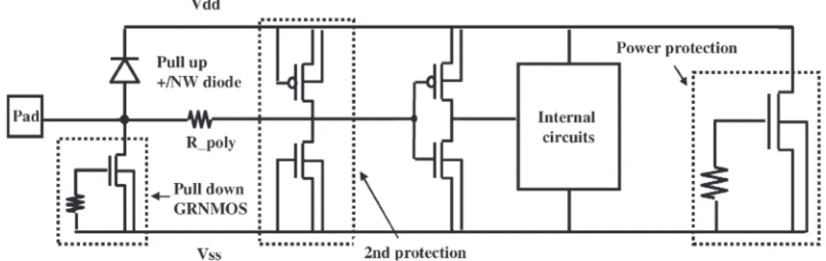
Fig. 6. Circuit schematic diagram of the LV input pin of TCG0002.
TABLE I
COMPARISON OFTESTRESULTS OFTCG0001ANDTCG0002. TCG0002 WASREVISEDFROMTCG0001TOIMPROVE THE
CBM IMMUNITY,AND THETESTLEVELISGREATLYIMPROVEDFROM750TO2000 V
the peak current of ESD. Fig. 5(a) and (b) shows the waveforms measured from the PCB’s golden pad and COF’s I/O pad by 100-V discharging, respectively. Clearly, the peak value at the golden pad measured from PCB is decreased and just about two times that from COF directly. Consequently, the parasiticRLC loading of the interconnection on PCB should be minimized to emulate a CBM event more accurately.
C. Chip-Level Design Guidelines for CBM Immunity
According to the previous studies [10], [11], same IC in different board positions or in different PCBs may have quite different failure rates subjected to the CBM ESD stresses. Also, ICs that are next to large insulators (plastic sockets or connectors) or close to PCB edges (corners, edge connectors, mounting holes, and test points) are more likely to suffer CBM ESD damage. These are probably the issues of field performance due to unknown customer PCB design and lay-out. However, what chip-level CDM performance should be designed for to ensure a certain CBM performance is a big question and challenge for ESD protection designers. Based on the results of many CBM experiments performed on source and gate driver ICs, the rule of thumb is that the TCP/COF CDM level should be larger than 1250 V to guarantee a two-digit DPPM failure rate for mass-produced LCD panels.
Additionally, according to the failure analysis results, the following design guidelines are proposed to improve the CBM immunity. First, the protection device should have better high second breakdown current and low voltage drop at the same time. Second, all the current paths from the anode to the cathode should strictly equalize the distances, and the contacts to anode diffusion edge spacing must be optimized to avoid filamentary damage due to current crowding and local high electric field. Last, the most important rule is to enhance the capability of power clamp cells as much as possible. The power pads can
become the major discharging paths during final testing after the panel’s assembly.
TCG0002 was revised from TCG0001 to improve the CBM immunity. A secondary protection cell with pull-up PMOSFET and pull-down NMOSFET was added between the resistor and input gate to enhance the gate oxide protection. Additionally, the pull-down diode and the PMOSFET power clamp were both changed to gate–resistor NMOSFET to increase the current-handling capability, as shown in Fig. 6. Table I shows the comparison of test results. The COF CDM test level is greatly improved from 750 to 2000 V. Also, the DPPM failure rate is smaller than 50.
IV. CONCLUSION
According to the aforementioned experimental results, the PCB evaluation board is not a must to emulate CBM ESD damage for large-sized chips, such as LCD driver ICs. The TCP/COF CDM test is proposed to directly emulate CBM dis-charging and successfully locate the weakest spot. Furthermore, to extract the correlation between the prefail voltages of PCB and TCP/COF emulations, the corresponding capacitance and discharging waveforms were measured. The results show that the parasiticRLC loading of interconnection on the PCB eval-uation board should be minimized to accurately emulate CBM ESD events. Finally, guidelines for chip-level cell design and layout optimization against CBM ESD damage are proposed and have been successfully implemented to improve the CBM immunity.
REFERENCES
[1] R. N. Shaw and R. D. Enoch, “An experimental investigation of ESD-induced damages to ICs on PCBs,” in Proc. EOS/ESD Symp., 1985, pp. 132–140.
[2] D. Pierce, “Can charged boards cause IC failure?” EOS/ESD Technol., pp. 7–8, Feb./Mar. 1988.
Proc. EOS/ESD Symp., 2002, pp. 250–256.
[10] A. Olney, B. Gifford, J. Guravage, and A. Righter, “Real-world charged board model (CBM) failures,” in Proc. EOS/ESD Symp., 2003, pp. 34–43. [11] J. Passi, H. Salmela, P. Tamminen, and J. Smallwood, “ESD sensitivity of devices on a charged printed wiring board,” in Proc. EOS/ESD Symp., 2003, pp. 143–150.
[12] J. Passi, “Electrostatic discharge of charged electronic modules,” in Proc.
2nd Nordic ESD Conf., Karlskoga, Sweden, Sep. 2006.
Jen-Chou Tseng received the B.S. degree from
National Chiao Tung University, Hsinchu, Taiwan, in 1992, the M.S. degree from the Institute of En-gineering and System Science, National Tsing-Hua University, Hsinchu, in 2000, and the Ph.D. de-gree from the Institute of Electronics Engineering, National Taiwan University, Taipei, Taiwan, in 2007. From 2000 to 2007, he was with Winbond Elec-tronic Corporation, Hsinchu, as a Deputy Manager in charge of the ESD/LU protection designs. In September 2007, he joined the Taiwan Semicon-ductor Manufacturing Corporation, Hsinchu, as a Manager of ESD/EOS engineering.
Chung-Ti Hsu received the B.S. and M.S.
de-grees from National Chiao Tung University (NCTU), Hsinchu, Taiwan, in 2001 and 2003, respectively, both in electronics engineering.
From 2003 to 2008, he was with Winbond Electronics Corporation, Hsinchu, where he worked on ESD/latch-up protection circuit design and ESD/LU failure analysis for logic/analog/RF/LCD driver/DRAM/Flash ICs. In July 2008, he joined Nuvoton Technology Corporation (spin-off from Winbond Electronics Corporation), Hsinchu, as a Technology Assistant Manager, leading the development of latch-up-free ESD protection designs in bipolar/CMOS/DMOS processes for Smart Power applications. He has published one technical paper in international journals and five papers in international conference proceedings. He is the holder of two Taiwan patents.
Taiwan, in 2006.
In 2006, she joined Winbond Electronic Cor-poration, Hsinchu, as an ESD Protection Design Engineer. In July 2008, she joined Nuvoton Technol-ogy Corporation (spin-off from Winbond Electronics Corporation), Hsinchu, and is responsible for on-chip ESD protection designs in various kinds of products. Her current research interests include ESD protection device development for Smart Power applications.
Ming-Dou Ker (S’92–M’94–SM’97–F’08) received
the Ph.D. degree from the Institute of Electronics, National Chiao Tung University, Hsinchu, Taiwan, in 1993.
He has been a Department Manager with the VLSI Design Division, Computer and Communi-cation Research Laboratories, Industrial Technol-ogy Research Institute, Hsinchu. Since 2004, he has been a Full Professor with the Nanoelectron-ics and Gigascale Systems Laboratory, Department of Electronics Engineering and Institute of Elec-tronics, National Chiao Tung University. From 2006 to 2008, he was the Director of the Master Degree Program of the College of Electrical En-gineering and Computer Science, National Chiao Tung University, and the Associate Executive Director of the National Science and Technology Pro-gram on System-on-Chip (NSoC Office), Taiwan. In 2008, he was the Chair Professor and Vice President of I-Shou University, Kaohsiung, Taiwan. He had been invited to teach and/or consult the reliability and quality de-sign for integrated circuits by hundreds of dede-sign houses and semiconduc-tor companies in the worldwide IC industry. He has published more than 330 technical papers on reliability and quality design for circuits and systems in CMOS technology in international journals and conference proceedings. He has proposed many inventions to improve the reliability and quality of integrated circuits. He is the holder of 136 U.S. and 143 R.O.C. (Taiwan) patents. His cur-rent research interests include reliability and quality design for nanoelectronics and gigascale systems, high-speed and mixed-voltage I/O interface circuits, on-glass circuits for system-on-panel applications, and biomimetic circuits and systems for intelligent prosthesis.
Prof. Ker was the President of Foundation of Taiwan ESD Association. He served as a member of the Technical Program Committee and the Session Chair of numerous international conferences. He also served as Associate Editor for the IEEE TRANSACTIONS ON VLSI SYSTEMS. He has been se-lected as a Distinguished Lecturer in the IEEE Circuits and Systems Society (2006–2007) and the IEEE Electron Devices Society (since 2008). In 2005, one of his patents on ESD protection design was awarded the National Invention Award in Taiwan.