I
鎳金屬誘發非晶矽薄膜側向結晶
鎳金屬誘發非晶矽薄膜側向結晶
鎳金屬誘發非晶矽薄膜側向結晶
鎳金屬誘發非晶矽薄膜側向結晶
-
-
-
-成長機制與低溫複晶矽薄膜電晶體效能之研究
成長機制與低溫複晶矽薄膜電晶體效能之研究
成長機制與低溫複晶矽薄膜電晶體效能之研究
成長機制與低溫複晶矽薄膜電晶體效能之研究
學生
學生
學生
學生:
::
:侯智元
侯智元
侯智元
侯智元
指導教授
指導教授:
指導教授
指導教授
::
:吳耀銓
吳耀銓
吳耀銓
吳耀銓
博士
博士
博士
博士
國立交通大學材料科學與工程研究所
國立交通大學材料科學與工程研究所
國立交通大學材料科學與工程研究所
國立交通大學材料科學與工程研究所
摘要
摘要
摘要
摘要
在本論文中,主要的研究是鎳金屬誘發非晶矽薄膜側向結晶。其中,探
討拉伸應力對於鎳金屬誘發非晶矽薄膜側向結晶成長機制之影響以及利用
鎳金屬壓印誘發結晶方法來製作低溫複晶矽薄膜電晶體。並結合鎳金屬誘
發非晶矽薄膜側向結晶與準分子雷射退火來製作高效能低溫複晶矽薄膜電
晶體。此外,為了解決對於鎳金屬誘發複晶矽薄膜來說,非常重要的鎳金
屬殘留問題,因而發展出有效的吸鎳方法來降低鎳金屬誘發複晶矽薄膜中
的鎳金屬殘留。
首先,鎳金屬誘發非晶矽薄膜側向結晶過程包括三個階段: (1)NiSi
2金屬
矽化物之生成,(2)在 NiSi
2金屬矽化物生成結晶矽之核,(3)藉由金屬矽化
物 NiSi
2之移動來產生非晶矽薄膜結晶與結晶成長。有相關報告指出,拉伸
應力會縮短鎳金屬誘發非晶矽薄膜側向結晶的潛伏時間。然而,其詳細的
II
機制並不清楚。在本實驗中,利用一簡單的彎曲設備來研究拉伸應力對鎳
金屬誘發非晶矽薄膜側向結晶之影響。基於實驗結果發現,拉伸應力並不
會影響 NiSi
2金屬矽化物與結晶矽核之生成,但是,會影響結晶矽之成長。
並發現壓應力並不影響鎳金屬誘發非晶矽薄膜側向結晶之速率。
鎳金屬壓印誘發結晶法比傳統鎳金屬誘發非晶矽薄膜側向結晶法存在著
許多更好的特性。在本實驗中,利用<111>與<112>不同成長方向之針狀結
晶來製作低溫複晶矽薄膜電晶體。<111>成長方向之針狀結晶是利用傳統鎳
金屬誘發非晶矽薄膜側向結晶來製作,而<112>成長方向之針狀結晶是利用
鎳金屬壓印誘發結晶方法來製作。結果發現,<112>成長方向之薄膜電晶體
在元件電特性優於<111>成長方向之薄膜電晶體,有 2.6 倍高的電子遷移
率,4 倍高的開/關電流比與 2.4 倍低的漏電流。
雖然,可以利用鎳金屬壓印誘發結晶之方法來製作元件特性較佳,均勻
性較好之低溫複晶矽薄膜電晶體。但是,在複晶矽針狀結晶間仍然存在著
許多的缺陷與未結晶區域,這些缺陷會使元件的特性劣化。結合準分子雷
射與鎳金屬壓印誘發結晶薄膜,來降低缺陷密度。並比較其薄膜電晶體之
特性,當雷射能量在 345 mJ/cm
2時,晶粒大小從 50 奈米增加到 250 奈米。
結合準分子雷射退火之電晶體,由於有較大的晶粒與較少的晶粒間之缺
陷,其電子遷移率為 413 cm
2/Vs,開/關電流比為 4.24×10
6,遠優於純粹壓
印結晶之電晶體。
III
最後,發展出兩種吸鎳的方法,來降低鎳金屬誘發側向結晶複晶矽薄膜
中的鎳金屬殘留。第一,利用厚度為 100 奈米的非晶矽薄膜來當作吸鎳層,
與厚度為 30 奈米的氮化矽來當做蝕刻停止層,在溫度為 550°C 下進行退火
90 小時來降低鎳金屬殘留。第二,利用鍍覆非晶矽薄膜之吸鎳基板與鎳金
屬誘發結晶之複晶矽薄膜接合並進行退火。其複晶矽薄膜中的鎳金屬殘留
可以被大大的降低。
IV
Ni-Metal Induced Lateral Crystallization of Amorphous Silicon
-
-
-
-
Growth Mechanism and LTPS TFTs Device Performance
Student: Chih-Yuan Hou Advisor: Dr. YewChung Sermon Wu
Department of Material Science and Engineering
National Chiao Tung University
Abstract
In this thesis, Ni-metal induced lateral crystallization (NILC) of amorphous silicon (α-Si) has been studied. The influence of tensile stress on the growth mechanism of NILC is investigated. Furthermore, we fabricate the LTPS TFTs by Ni-metal imprint-induced crystallization method. Combine NILC and excimer laser annealing (ELA) method to produce high-performance LTPS TFTs. Moreover, in order to solve this issue of NILC poly-Si film, we develop an effective gettering method to reduce the Ni-metal impurity contamination of the NILC poly-Si films.
Initially, three stages have been identified in the NILC process: (1) the formation of NiSi2
precipitates, (2) the nucleation of crystalline Si (c-Si) on NiSi2 precipitates, and (3) the
subsequent migration of NiSi2 precipitates and growth of c-Si. It has been reported that the
V
clarified. In this study, a simple bending fixture was used to investigate the effects of tensile stress on the growth of NILC. Base on the results of this study, it was found that tensile stress did not enhance NiSi2 formation and c-Si nucleation stages, but enhanced the c-Si growth
stage. It was also found that compressive stress did not change NILC rate.
The Ni-metal imprint-induced crystallization method exhibited many superior characteristic over traditional NILC method. In this study, for the LTPS TFTs fabricated using <111> and <112> needle grains have been investigated. They were fabricated by traditional NILC and Ni–metal imprint-induced crystallization method. It is found that the performance of 112-TFT was far superior to that of 111-TFT. The device transfer characteristics of 112-TFT include 2.6-fold-higher field-effect mobility (µFE), 4-fold-higher on/off current ratio (ION/OFF), and
2.4-fold-lower leakage current (IOFF) compared with those of the 111-TFT.
The improved performance and good uniformity LTPS TFTs have been fabricated using Ni-metal imprint-induced crystallization method. However, the polycrystalline silicon film contained many intra-grain defects with some un-crystallized regions between poly-Si needle grains. These defects degrade the transfer characteristics of TFT devices, including the field effect mobility (µFE) and the leakage current. In this study, combine the excimer laser
VI
and IMPRINT-ELA TFT, upon increasing the laser energy to 345 mJ/cm2, the grain size increased from 50 to 250 nm and the performance of IMPRINT-ELA-TFT was found to be far superior to that of IMPRINT-TFT due to larger grains and fewer intra-grain defects of the IMPRINT-ELA poly-Si film than that of the IMPRINT poly-Si film. The mobility of the IMPRINT-ELA-TFT was 413 cm2/Vs, which was 31.7 times higher than that of the IMPRINT-TFT. The on/off current ratio of the IMPRINT-ELA-TFT was 4.24 ×10⁶, which was 2 orders magnitude higher than that of the IMPRINT-TFT.
Finally, develop two gettering methods to reduce the Ni contamination within the NILC poly-Si film. First, using α-Si films with a thickness of 100 nm as a Ni-gettering layer, silicon-nitride (SiNx) films with a thickness of 30 nm as the etching stop layers and annealed
at 550°C for 90 h to reduce the Ni-metal impurity within the NILC poly-Si film. Second, an α-Si-coated wafers used as Ni-gettering substrates then bonding the gettering substrate and NILC poly-Si film together. The Ni-metal impurity within the NILC poly-Si film was greatly reduced.
VII
Table of Contents
Abstract (Chinese)
………...…..…………...IAbstract (English)
……….……...IVTable of Contents
………...…...VIITable Lists
………...…………...XIFigure Captions
………..………….XIIChapter 1 Introduction………..1
1-1 Overview of Thin-Film Transistors (TFTs)……….1
1-1-1 Amorphous Silicon (α-Si) TFTs………..3
1-1-2 Low-Temperature Polycrystalline Silicon (LTPS) TFTs………....4
1-2 Low-Temperature Polycrystalline Silicon Crystallization (LTPS) Methods……..6
1-2-1 Solid Phase Crystallization (SPC) Method………...7
1-2-2 Excimer Laser Annealing (ELA) Method……..……….…………..8
1-2-3 Ni-Metal Induced Crystallization (NIC) / Ni-Metal Induced Lateral Crystallization (NILC) Method……….………..10
1-3 Electrical Characteristics of Ni-Metal Induced Lateral Crystallization (NILC) Thin Film Transistors……….………16
VIII
Chapter 2 Effects of Tensile Stress on Growth of Ni-Metal Induced Lateral
Crystallization of Amorphous Silicon……….30
2-1 Growth Mechanism of Ni-Metal Induced Lateral Crystallization (NILC)……...30
2-2 Experimental Procedure………32
2-2-1 Features of the Bending Fixture………...32
2-2-2 Preparation for the Bending Sample………34
2-3 Results and Discussion………..35
2-3-1 OM and SEM Analysis………35
2-3-2 A Series Two-Step Annealing for NILC……….37
2-3-3 Mechanism for the Effects of Tensile Stress on the Growth of NILC……41
2-4 Summary………...44
Chapter 3 Performance of NILC Thin-Film Transistors with <111> and
<112> Needle Grains………....47
3-1 Different Method for NILC of Amorphous Silicon……….47
3-2 Experimental Procedure………...49
3-2-1 Preparation of the Imprint Mold……….50
IX
3-3 Results and Discussion………...53
3-3-1 Scanning Electron Microscopy (SEM) and Transmission Electron Microscopy (TEM) Analysis………....53
3-3-2 Electrical Characteristics of 111-TFTs and 112-TFTs………..57
3-4 Summary……….60
Chapter 4 Comparison of LTPS TFTs Made by IMPRINT and
IMPRINT-ELA Methods………63
4-1 The Conception of the Post Laser Treatment………..63
4-2 Experimental Procedure………..64
4-2-1 Fabrication of the IMPRINT-ELA Polycrystalline Silicon Films……….64
4-2-2 Fabrication of the IMPRINT-ELA TFTs………...67
4-3 Results and Discussion………69
4-3-1 Microstructure Analysis of Polycrystalline Films……….69
4-3-2 Electrical Characteristic of the IMPRINT and IMPRINT-ELA TFTs...73
X
Chapter 5 Gettering of Nickel from the NILC Polycrystalline Silicon
Films………...81
5-1 The Conception of the Gettering Method………...81
5-2 Gettering of Nickel within the NILC Polycrystalline Silicon Films Using α-Si Film……….………..84
5-2-1 Introduction………....………84
5-2-2 Experimental Procedure……….84
5-2-3 Results and Discussion……….………..87
5-2-4 Summary……….93
5-3 Gettering of Nickel from NILC Poly-Si Films Using a Gettering Substrate….94 5-3-1 Introduction………94
5-3-2 Experimental Procedure……….94
5-3-3 Results and Discussion………...96
5-3-4 Summary………...102
XI
Table List
Chapter 2
Table I
Summary of two-step processes for Ni–NILC of α-Si.Chapter 3
Table I
Specifications and fabrication methods of 111-TFT and 112-TFT.Table II
Device characteristics of 111-TFT and 112-TFT.Chapter 4
Table I
Summary of device characteristics of IMPRINT-TFT and IMPRINT-ELA-TFT with a laser energy density of 345 mJ/cm2.XII
Figure Captions
Chapter 1
Fig. 1-1
Circuit diagram of an active matrix liquid crystal display (AMLCD).Fig. 1-2
Roadmap of poly-Si TFT technology.Fig. 1-3
Illustration of transformation scenarios during the ELA process. Correspond to (a) partial melting, (b) completely melting and (c) near-completely melting of the initial Si film.Fig. 1-4
Solidification of the molten Si film. Resulting in the higher surface roughness.Fig. 1-5
Schematic illustration of the Ni-metal induced Crystallization (NIC) and Ni-metalinduced lateral crystallization (NILC).
Fig. 1-6
Schematic representation of favorable precipitate orientations for long-range growth of epitaxial Si within the plane of the α-Si.Fig. 1-7
Schematic equilibrium molar free-energy diagram for NiSi2 in contact with α-Si.Fig. 1-8
Schematic representation of a possible growth mechanism involving the formation of a thin layer of c-Si at the NiSi2/α-Si interface.Fig. 1-9
The band diagram for the leakage current model. (a) Case of weak electric field. (b) Case of medium electric field. (c) Case of strong electric field.XIII
Chapter 2
Fig. 2-1
Schematic equilibrium molar free-energy diagram for NiSi2 in contact with α-Si.Fig. 2-2
Schematic illustration of stainless bending fixture, (a) BENDED (tensile) sample and UNBENDED sample, and (b) compressed sample. The side view shows the sample structure and the top view the location of the Ni line pattern.Fig. 2-3
Flow chart of the sample preparation.Fig. 2-4
(a) Optical microscopy image of BENDED sample annealed at 550°C for 6 h. (b) SEM image of NILC front region of BENDED sample annealed at 550°C for 6 h.Fig. 2-5
Illustration of the NILC growth length (BENDED sample) related to the positionof Ni lines.
Fig. 2-6
Optical microscopy (OM) image of the NILC growth length (BENDED sample) related to the direction between Ni line and bending direction.Fig. 2-7
Photograph of bended sample annealed at 550°C for 6 h. The sample was bent due to plastic deformation.Fig. 2-8
NILC growth length as function of annealing time.Fig. 2-9
NILC poly-Si formation mechanism. (a) shows that Ni atoms and NiSi2 diffuse/migrate to the a-Si region. (b) shows the schematic illustration of the atomic jump process. (c) shows the schematic illustration of free energy as a function of reaction coordinate as an atom moves from one site to another. In thisXIV
case the reaction coordinate corresponds to the distance along the path connecting the sites.
Chapter 3
Fig. 3-1
Schematic illustration of the Ni-metal induced Crystallization (NIC) and Ni-metal induced lateral crystallization (NILC).Fig. 3-2
Schematic illustration of Ni-metal imprint method.Fig. 3-3
Imprint mold preparation process flow.Fig. 3-4
SEM image of imprint mold.Fig. 3-5
Optical microscopy image of 112-poly-Si annealed at 550°C for 24 h.Fig. 3-6
(a) SEM image of Secco-etched 111-poly-Si film and (b) TEM image of 111- poly-Si film.Fig. 3-7
NILC growth length as a function of annealing time. For different crystallization method involved of 112-poly-Si and 111-poly-Si.Fig. 3-8
(a) SEM image of Secco-etched 112-poly-Si film and (b) TEM image of 112- poly-Si film. Compared with 111-poly-Si, 112-poly-Si had fewer branch grains and less un-crystallized α-Si. The preferred direction of needlelike Si grains was <112>, which differed from that of 111-poly-Si grains, <111>.XV
112-poly-Si grains.
Fig. 3-10
Typical IDS-VGS transfer characteristic of 111-TFT and 112-TFT.Fig. 3-11
Schematic illustration of growth of needle grains: (a) 112–poly-Si and (b) 111-poly-Si grains. All 112-poly-Si grains were parallel to each other with the exception of very few branch grains between them.Chapter 4
Fig. 4-1
(a) The Schematic illustration of Ni-imprint method. (b) SEM image of imprint mold.Fig. 4-2
Illustration of the Ni-metal imprint poly-Si with post excimer laser treatment.Fig. 4-3
Setup of excimer laser annealing system.Fig. 4-4
Flow chart of TFT device fabrication process.Fig. 4-5
(a) The SEM image of Secco-etched Ni-imprint poly-Si film. The needle grains were parallel to each other. (b) The TEM image and the corresponding diffraction pattern of the Ni-imprint poly-Si.Fig. 4-6
(a) Grain size versus laser energy density. (b) The SEM image of Secco-etched IMPRINT-ELA poly-Si film.Fig. 4-7
The Transfer characteristics of IMPRINT-TFT and IMPRINT-ELA-TFT with a laser energy density of 345 mJ/cm2.XVI
Chapter 5
Fig. 5-1 Schematic illustration of basic NILC fabrication process of both poly-Si films. (a) is
the α-Si/SiO2. (b) is the 2 nm Ni thin film deposited on the top of α-Si. (c) is the
α-Si coated with Ni pads to form the NILC poly-Si. (d) is the NILC poly-Si islands.
Fig. 5-2 Schematic illustration of the gettering process. (a) is the α-Si coated with Ni pads to
form the NILC poly-Si. (b) is the NILC poly-Si islands. (c) is the NILC poly-Si coated with etching stop layer (SiNx) and gettering layer (α-Si). They were then
annealed at 550°C for 90 h to carry out the gettering process. (d) is the GETR poly-Si (after removed the SiNx and α-Si layers).
Fig. 5-3 (a) is OM image of sample after annealing at 550°C for 24 h. (b) is SEM image of
NILC poly-Si front region (after Secco etching). (c) is TEM image of NILC poly-Si grains.
Fig. 5-4
(a) Schematic illustration of the silicide-etching holes at the boundaries where two poly-Si fronts intersected. SEM image of these etching holes were shown on (b) and (c). (b) is the NILC poly-Si. (c) is the GETR poly-Si.Fig. 5-5 (a) OM and (b) SEM images (after Secco etching) of the gettering layer (Si film).
Fig. 5-6 SIMS depth profile of nickel in the poly-Si film. The dash line is the GETR POLY;
XVII
Fig. 5-7
Schematic illustration of the gettering process. (a) is the NILC POLY and the Ni- gettering substrate coated with α-Si films. (b) is the NILC POLY bonded to the Ni-gettering substrate. They were then annealed at 550°C for12 h to carry out the gettering process. (c) is to separate two substrates. (d) is the Ni-gettering substrate recycled process. The Si-films on the surface of the gettering substrate was polished or etched away. Again, α-Si films were deposited onto the wafers as Ni-gettering substrate.Fig. 5-8 (a) is OM image of the NILC POLY film. (b) is SEM image of NILC poly-Si front
region (after Secco etching).
Fig. 5-9
(a) Schematic illustration of the silicide-etching holes on the NIC areas and grain boundaries of the NILC POLY film. SEM image of these etching holes were shown on (b) and (c), respectively.Fig. 5-10 SIMS depth profile of nickel in the poly-Si film. The dash line is the GETR POLY;
the real line is the NILC POLY, respectively.
Fig. 5-11 (a) OM and (b) SEM images (after Secco etching) of the inner-side Si film on the
1
Chapter 1 Introduction
1-1
Overview of Thin-Film Transistors (TFTs)
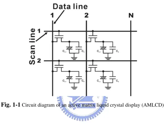
Thin-film field-effect transistors (TFTs) utilize the modulation of conductivity of a semiconductor film by the voltage of an insulated gate. In contrast with the metal-oxide semiconductor field-effect transistor (MOSFET) the TFTs can be made using thin films of either amorphous or polycrystalline semiconductors. As the TFTs do not require single crystal semiconductor material, it can be fabricated on a variety of insulating substrates. The major application for the TFTs at present is in active matrix flat panel displays (AMFPD). A circuit diagram of an active matrix liquid crystal display is shown in Fig. 1-1. Each pixel consists of a capacitor with liquid crystal material as the dielectric (CLC), storage capacitor (CS) and a
switching transistor. TFTs are turned on by applying a voltage to single row (scan line). Then, the signal is transferred to the capacitor (pixel) from the data line. The liquid crystal material rotates the polarization of light to a degree, which depends on the applied electric field. The intensity of transmitted light is thus determined by the signal applied to the data line. When the gate voltage is returned to zero, the signal remains on the capacitor for a time determined
2
by the leakage current (Ilk) of the TFTs. The leakage current should be low enough so
grayscale levels can be maintained over the frame refresh time.
Fig. 1-1 Circuit diagram of an active matrix liquid crystal display (AMLCD).
Thin-film transistors is a fundamental component of AMFPD; therefore, to investigate the TFTs is very important for the development of flat panel display technology.
3
1-1-1
Amorphous Silicon (α-Si) TFTs
Compare to the conventional cathode ray tube (CRT) display, the flat panel display has light weight and small volume. Among many productive flat panel display, the active matrix liquid crystal display (AMLCD) have widely use in many applications, such as laptop and desktop monitor. Today, the α-Si TFT-LCDs have dominated the large area flat panel display market. The TFT-LCDs have become the standard component of laptop, desktop monitor and digital camera.
Active matrix liquid crystal display fabricated on α-Si TFTs is the most usual technique, due to the advantages such as low temperature process (<350°C), [1.1,1.2] suitable for large area, non-expensive glass substrate and lower leakage current, that is enabling for pixel switching. Nevertheless, the α-Si TFTs exhibited poor field-effect carrier mobility (typically µFE< 1 cm2/V-s) and smaller on current. This is due to the poor electrical performance of the
α-Si TFTs. To achieve the needed current flow for the grayscale of the frame, the dimension of α-Si TFTs device was increased. Resolution of the display will be decreased resulted from the large α-Si TFTs. The high-resolution TFT-LCD needs new solution to improve the mobility of TFTs. The poly-Si TFTs technology is one of the potential methods to achieve the requirement of high-resolution TFT LCD. And the poor field-effect carrier mobility can be overcome easily using the poly-Si films as the active layer of the TFTs.
4
1-1-2
Low-Temperature Polycrystalline Silicon (LTPS) TFTs
In 1980, high temperature polycrystalline silicon TFTs had been introduced.[1.3] They used chemical-vapor deposited poly-Si to achieve good carrier mobility and electrical characteristics. With mobility around 50 cm2/V-s, these high temperature poly-Si TFTs were employed gate insulator SiO2 grown thermally at 1050°C. This approach requires a high strain
temperature substrate such as quartz, incompatible with the commercially available large area non-expensive glass substrate.
Recently, many researchers have developed various techniques for crystallization of α-Si at low temperature (below 600°C), and then transformation it to poly-Si; the motivation for pushing up the mobility to be able to integrate drive circuitry [1.4,1.5] as well as providing pixel TFTs and more compatible with the glass substrate. In fact, the field effect mobility of poly-Si TFTs is significantly higher than that of α-Si about two orders of magnitudes. The higher drive current allows small TFTs dimension to be used as the pixel switching elements, resulting in higher aperture ratio and lower parasitic gate-line capacitance for improved display performance. [1.6]
Unlike MOSFETs, where the active layer is part of the substrate, in the case of TFTs the active layer needs to be separately formed on the host substrate. The crystallization method affect the microstructure quality of the resulting poly-Si film, which means that the performance of poly-Si TFT will be affected by the selection of techniques for the
5
crystallization of Si films.
A various techniques have been investigated for crystallization of α-Si at low temperature such as: (1) solid phase crystallization (SPC) (2) excimer laser Annealing (ELA) (3) Ni-metal induced/Ni-metal induced lateral crystallization (NIC/NILC). In the following section, we will review the crystallization method that the above-mentioned.
6
1-2
Low-Temperature
Polycrystalline
Silicon
(LTPS)
Crystallization Method
Crystallization of α-Si films has been considered as the most important process step in the fabrication of LTPS TFTs. The quality of crystallized poly-Si films is quite sensitive to the performance of poly-Si TFT. In poly-Si films, most defects are generated at the grain boundaries. Enlarging the grain size can promote the quality of poly-Si, as deposited poly-Si generally exhibits small grain size. In general, the poly-Si crystallized from α-Si usually has larger grain size than that of as-deposited poly-Si. Historically, solid phase crystallization [1.7] was the first technology to produce poly-Si films for display applications, followed by laser crystallization. The ultimate goal of the LTPS technology is to integrate the pixel-driving circuits on the display substrate. Fig. 1-2 shows the anticipated evolution of poly-Si technology development and its impact on the degree of on-panel integration.[1.8]
7
1-2-1
Solid Phase Crystallization (SPC) Method
Deposited α-Si thin films were transformed to poly-Si using SPC method has obtained better TFT device electrical performance [1.9] than as-deposited poly-Si films. For the SPC method, α-Si films are crystallized in a furnace at temperature about 600°C for duration time (about 24 h). The polycrystalline grains are generally in oval-shaped, and large defect density exists in poly-Si films. Amorphous Si is a thermodynamically meta-stable phase possessing a driving force for transformation to polycrystalline phase given a sufficient energy to overcome the initial energy barrier.
A key factor affecting crystallization is the nucleation rate in the α-Si films. The nucleation rate is strongly influenced by the selected deposition method and condition. [1.10,1.11] The structural order/disorder in the α-Si films affects the films to form stable nuclei. Higher disorder structure increases the energy barrier required to form the Si nuclei; this concept has been used in the past to increase the grain size of poly-Si films. Ideally, a small number of fast-growing nuclei are needed to maximize the grain size. However, the reality of the situation is that the probability that additional nucleation events will occur within the volume separating growing nuclei increases geometrically with the separation distance.
8
1-2-2
Excimer Laser Annealing (ELA) Method
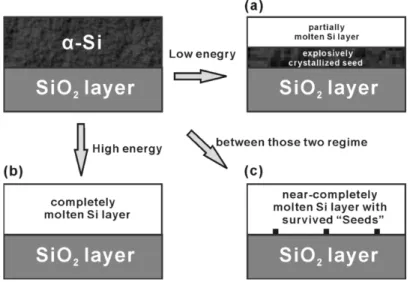
Excimer laser annealing is suitable for fabrication of LTPS TFTs on large area glass substrate. Development of the ELA method has provided poly-Si material with high quality than SPC method. This is attributed to the melt-induced poly-Si growth. For the crystallization process, the laser is irradiated at the α-Si and the silicon is heated above 1200°C. However, only sustained for a very short time; therefore, it will not damage the glass substrate. Moreover, as shown in Fig. 1-3, there are two major transformation regimes (occurring at low and high laser energy, respectively) and one minor transformation regime in between (that so-called superlateral growth, or SLG).[1.12,1.13] The low laser energy regime describes a situation where the incident laser is sufficient to induce melting of the silicon films, but it is low enough that a continuous layer of silicon at the maximum extent of melting. For this reason, this regime is referred to as the partial melting regime. The high laser energy regime corresponds to a situation that the laser energy is sufficiently high to completely melt the silicon film; this regime is also referred to as complete melting regime. In addition to these two regimes, a third regime has been found to exist within a very narrow experimental window in between the two main regimes. Despite the small extent of this region, it is nonetheless one with great technological significance, because the poly-Si films within the regime feature large-grained polycrystalline microstructures.[1.14] The stable grain size of ELA poly-Si films is typically limited to 0.3~0.6 µm. Larger grain size is possible within the
9
SLG window, but this regime is intrinsically unstable.
Fig. 1-3 Illustration of transformation scenarios during the ELA process. Correspond to (a)
partial melting, (b) completely melting and (c) near-completely melting of the initial Si film.
The surface roughness in ELA poly-Si films is localized at the planes and point of congruence of grain boundaries. The mechanism for the formation of roughness is well understood and is attributed to the specific density difference between molten Si (2.53 g cm-3) and solid Si (2.30 g cm-3). In other words, as the molten Si solidifies, it simultaneously expands. Solidification starts from neighboring seed areas, and the last region to solidify is the volume at the vicinity of the two colliding lateral fronts. As that happens, the generated solid Si can only expand upward, as shown in Fig. 1-4, thus generating the ridge associated with the formation of the grain boundary at the location.
10
Fig. 1-4 Solidification of the molten Si film. Resulting in the higher surface roughness.
Although the highest quality poly-Si films were fabricated by ELA method, the poor grain size uniformity and high roughness ELA poly-Si films degraded the performance of TFT.[1.15]
1-2-3
Ni-Metal Induced Crystallization (NIC) / Ni-Metal
Induced Lateral Crystallization (NILC) Method
Solid phase crystallization of α-Si needed a high temperature and longer annealing time for furnace annealing process. In the NIC/NILC method,[1.16~1.19] the annealing time and temperature could be reduced, and the grain size of NILC poly-Si films uniformly over large area could be obtained. In 2000, Sharp Corp. and SEL (Semiconductor Energy Lab.) propose the CGSi (Continuous Grain Silicon) technique to fabricate the 60 inch HDTV rear
11
projector.[1.20] When thin Ni is deposited on α-Si and annealed, Ni disilicide (NiSi2)
forms.[1.21] The nickel disilicide is cubic with CaF2 structure and has a very close lattice
parameter match to c-Si (-0.4%), the lattice constant of NiSi2, 5.406A, is nearly equal to that
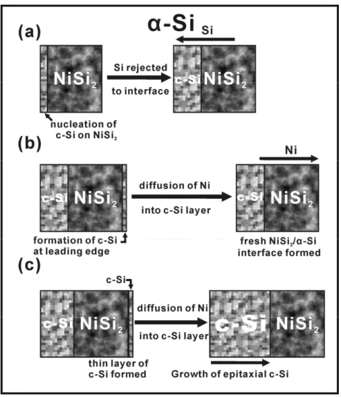
of Si, 5.430A. The disilicide is actually the species that mediates the transformation of α-Si to c-Si. As shown in Fig. 1-5, the c-Si formed below the Ni-pad is called NIC and the lateral growth is called NILC.
Fig. 1-5 Schematic illustration of the Ni-metal induced Crystallization (NIC) and Ni-metal
induced lateral crystallization (NILC).
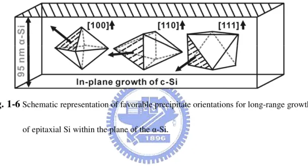
The silicide mediate growth of silicon occurs in three stages. In the first stage, precipitation and growth of NiSi2 occur in the temperature range of 325~400°C. In the second phase,
crystalline Si nucleates on one or more the eight {111} faces of the octahedral NiSi2, as
shown in Fig. 1-6. Finally, in the third phase, c-Si growth proceeds with a NiSi2 precipitate at
12
As shown in Fig. 1-6, for <110>-oriented precipitates, four of the {111} planes exhibit surface normal within the planes of the film, which makes extensive growth possible. On the other hand, the <100>- and <111>-oriented precipitates exhibits {111} planes normal that intersect the upper and lower surface of α-Si films.
Fig. 1-6 Schematic representation of favorable precipitate orientations for long-range growth
of epitaxial Si within the plane of the α-Si.
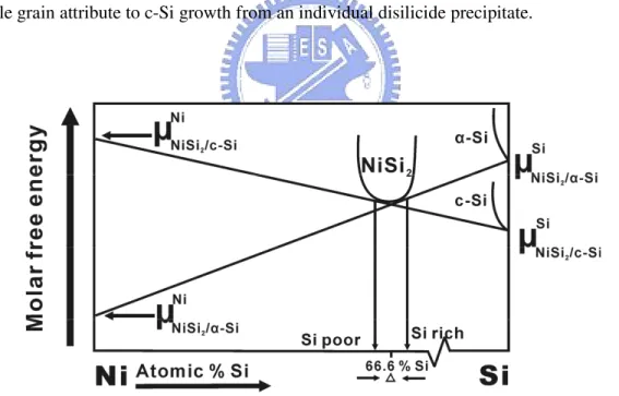
The driving force for the migration of NiSi2 precipitates is reduction in the free energy
associated with the transformation of meta-stable α-Si to stable c-Si. An equilibrium free-energy diagram is provided for explanation, as shown in Fig. 1-7.[1.21] It is well known that the α-Si has a higher free energy than c-Si. In the case of Ni silicide mediated crystallization, the free energy difference between Ni and Si atoms at the NiSi2/α-Si and
NiSi2/c-Si interface acts as the driving force for Ni diffusion.[1.21] The free energy of the Ni
13
energy of the Si atom is lower at the NiSi2/c-Si interface. Therefore, with the dissociative
model,[1.21] the NiSi2 layer dissociates to provide free Si for epitaxial growth of c-Si at the
c-Si/NiSi2 interface by the diffusion of Ni atoms. The Ni atoms diffuse to α-Si following by
formation of a fresh NiSi2/α-Si interface. Repetition of this process results in migration of
NiSi2 precipitates through α-Si and growth of needlelike Si. Fig. 1-8 shows a schematic
representation of a possible growth process incorporating the formation of intermediate thin layer of c-Si on the leading edge of migrating NiSi2 precipitate.[1.21] As a result of this
growth mechanism, NILC poly-Si films demonstrate a needlelike microstructure, with each needle grain attribute to c-Si growth from an individual disilicide precipitate.
Fig. 1-7 Schematic equilibrium molar free-energy diagram for NiSi
2 in contact with α-Si.14
enhancing Si crystal growth. These include Au[1.22], Al[1.23] and Sb[1.24] which form eutectic with Si, and Pd[1.25,1.26], which form silicide with Si.
Fig. 1-8 Schematic representation of a possible growth mechanism involoving the formation
15
As a result, Ni remains the undisputed metal of choice for silicide-assisted crystallization. It should be noted that traces of NiSi2 also remain within the c-Si that is left behind after the
growth phase. This would have presented an insurmountable obstacle had it not been for the existence of an efficient gettering process.[1.27,1.28] This process utilizes the implantation of phosphorous, followed by low-temperature annealing to generate electrically inactive compounds. Previous studies have demonstrated the effectiveness of the gettering process in removing the remaining silicide in the film after Si crystallization.[1.20,1.29] In practice, the necessity to maintain a low processing temperature poses certain limitations on the quality of the poly-Si microstructure. One way to boost the poly-Si quality is by combining NILC with laser annealing process [1.30,1.31] to produce high quality and good uniformity poly-Si films to realize the system-on-panel technology.[1.8,1.32-1.33]
In this thesis, we will focus on the Ni-metal induced lateral crystallization method. To discuss the growth mechanism of NILC and utilized Ni-metal imprint induced crystallization method[1.34] to fabricate the LTPS TFT. Moreover, to produce high performance LTPS TFTs by combined Ni-metal imprint and ELA method. And develop a simple method to getter the nickel impurity within the NILC polycrystalline silicon films.
16
1-3
Electrical Characteristics of Ni-Metal Induced Lateral
Crystallization (NILC) Thin Film Transistors
The NILC method has some advantages over other crystallization methods such as: lower equipment cost, better uniformity than ELA method, and lower thermal budget than SPC method. However, several intrinsic growth characteristics of NILC method always resulted in poor TFT performance, such as higher leakage current (Ilk) and poor electrical stability due to
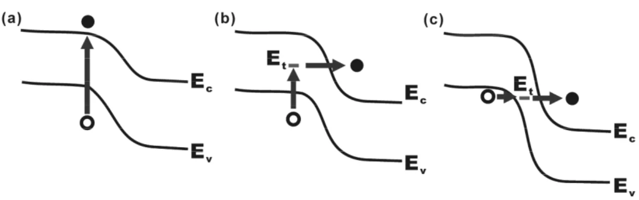
large defect (trap state) density in NIC/NILC interface and NILC/NILC grain boundary and high Ni metal contamination.[1.35~1.39] Fig. 1-9 illustrates the leakage current model using band diagrams,[1.40-1.42] the first situation in Fig. 1-9 (a) is described only the thermal activation of an electron from the valence band to the conduction band. The second situation in Fig. 1-9 (b), the leakage current is induced by the trap or surface state in the band gap. With increase the drain bias, the activation energy of leakage current decreases, which suggests that the high field in the drain depletion region has reduced the barrier that the electron must overcome. This situation comprises two steps: the first step is the thermal activation of an electron from the valence band to a trap state (Et) in the band gap, and the second step is
electron tunneling through this reduced barrier to the conduction band. As such, the dominant leakage current mechanism is thermionic field emission. The third situation in Fig. 1-9 (c) is induced under strong electric field, in which the dominant leakage current mechanism is pure tunneling. With the increase of the electric field, the tunneling length decreases. The presence
17
of the trap state in the band gap assists the process by shorting the effective tunneling length of the electron. In addition, the trap state in the band gap plays an important role in the leakage current model. In the traditional MOSFET, those situations do not occur easily because the trap state is low. This causes different leakage current between MOSFET and TFTs.
Moreover, the Ni contamination of the NILC poly-Si films can degrade the minority carrier life time and increase the leakage current. The leakage current is proportional to the impurity concentration. [1.43,1.44]
In order to solve the above problems, the post-annealing treatment [1.30,1.45-1.47] was
Fig. 1-9 The band diagram for the leakage current model. (a) Case of weak electric field. (b)
18
proposed to reduce the NILC/NILC grain boundary defect density. Moreover, gettering process [1.20,1.29] was proposed to reduce the Ni-metal contamination within the NILC poly-Si films. In the following, we will discuss the effects of grain boundary and Ni-metal impurity on the electrical performance of NILC TFTs.
19
1-4
Motivation and Thesis Organization
In this thesis, the major research subject is Ni-metal induced lateral crystallization of
amorphous silicon, which involved of the tensile stress effects on the NILC growth mechanism. It has been reported that the Ni-metal imprint method introduced a tensile stress, while the crystallization process and the incubation time could be reduced by tensile stress. However, the detail of the tensile stress effects on the growth mechanism of NILC has still not been clarified. In addition, in this study, we chose the Ni-metal imprint-induced crystallization method due to it exhibited many superior characteristics over traditional NILC method, such as: higher growth rate, better crystallization quality and less branch needle-like grain microstructure. But, between the NILC/NILC needle-like gains contained many un-crystallized region; these intra-grain defects can degrade the device performance. Therefore, combine NILC and ELA method to gather the advantages of each method, producing the high performance TFTs device. Finally, the most important issue for the NILC poly-Si film is the Ni-impurity contamination. To develop a simple gettering method for reduced the Ni-impurity within the NILC poly-Si films.
In chapter 2, the influence of tensile stress on the growth of NILC of α-Si was investigated by using a simple bending fixture. Before the growth of needlelike poly-Si grains, there must be an incubation period, which included (1) the formation of NiSi2 and (2) the nucleation of
20
However, the detail of the tensile stress effects on the growth mechanism of NILC has still not been clarified. The principal goal of this research, therefore, was to develop a series of two-step annealing processes to study the effects of tensile stress on these three stages of NILC growth.
In chapter 3, using the Ni-metal imprint method to crystallized α-Si and fabricated the TFTs device. For traditional NILC method, Crystalline Si nucleates on {111} faces of NiSi2.
The crystallization of needlelike Si grains proceeds via the migration of nickel silicides through α-Si. The orientation of needle grain is <111>. Unfortunately, the NILC poly-Si film has intra-grain defects and some un-crystallized regions between poly-Si grains. In this chapter, these defects were reduced by Ni-metal imprint induced crystallization method. In Ni-metal imprint method, a thin Ni metal layer was deposited on the imprint mold. The mold and α-Si film were then pressed together and annealed at 550°C. The orientation of Ni-metal imprint needle grains is <112>, which differed from that of NILC needle grains <111>. Therefore, the principal goal of this chapter has been to investigate the performances of TFTs fabricated by <112> and <111> needle grains.
In chapter 4, among various crystallization technologies, excimer laser crystallization (ELA) and Ni-metal induced lateral crystallization have shown to be most two promising techniques to produce high quality poly-Si thin films at low temperature. There are still some problems about those two methods, especially for LTPS TFTs applications. In this study, combining the
21
Ni-metal imprint and ELA method, to produce high quality poly-Si films with good uniformity and reduced the intra-grain defect density within the NILC poly-Si films using excimer laser for post-crystallization to improve the electrical characteristics.
Some intrinsic growth characteristics of NILC technique can degrade the performance of TFTs device. As mention in the last chapter, the intra-grain defects can be reduced using post-crystallization technique. Besides, the reduction of Ni contamination within the NILC poly-Si films is also a very important issue. Therefore, in chapter 5, two gettering methods have been utilized to reduce the Ni impurity within the NILC poly-Si film. Those two gettering process are uncomplicated, one is using a SiNx/α-Si and the other is using α-Si/Si substrate as the gettering material. Use the un-doped silicon layer to prevent other impurity contamination and more compatible for the TFTs fabrication process.
Finally, conclusions as well as the recommendation for the further research are given in Chapter 6.
22
Reference:
[1.1] H. Gleskova, S. Wagner, V. Gasparik, and P. Kovac, "150°C Amorphous Silicon Thin-Film Transistor Technology for Polyimide Substrates." J. Electrochem. Soc., vol. 148, pp. G370-G374, 2001.
[1.2] K. Long, A. Z. Kattamis, I.-C. Cheng, H. Gleskova, S. Wagner, and J. C. Sturm, "Stability of Amorphous-Silicon TFTs Deposited on Clear Plastic Substrates at 250°C to 280°C." IEEE Electron Device Lett., vol. 27, pp. 111-113, 2006.
[1.3] S.W. Depp, A. Juliana, and B. G. Huth, "Polysilicon FET Devices for Large Area Input/Oput Applications." Proc. IEMD, vol. 26, pp. 703-706, 1980.
[1.4] M. Matsuo, T. Hashizume, S. Inoue, M. Miyasaka, S. Takenake. I. Yudasaka, and H. Oshima, "1.3-in. Full-color VGA poly-Si TFT-LCDs with completely integrated drivers." SID Symposium Dig., vol. XXV, pp. 87-90, 1994.
[1.5] S. Inue, M. Matsuo, K. Kitawada, S. Takenaka, S. Higashi, T. Ozawa, Y. Matsueda, T. Nakazawa, and H. Oshima, "425°C Poly-Si TFT technology and its applications to large-size LCDs and integrated digital data drivers." Proceedings of the 15th IDRC, pp. 339-342, 1995.
[1.6] I-W Wu, "Celldesign considerations for high aperature ratio direct view and projection polysilicon TFT-LCD." in SID Tech. Dig., pp. 19-21, 1995.
23
Miyita, and H. Kawakami, "High-performance low-tmeperature poly-Si n-channel TFTs for LCD." IEEE Trans. Electron Dev., vol. 36, pp. 351-359, 1989.
[1.8] T. Voutsas, P. Schuele, B. Crowder, P. Joshi, R. Sposili, H. Kisdarjono, T. Afentakis, J. Hartzell, “Next generation of poly-Si TFT technology: material improvements and novel device architectures for system-on-panel (SOP).” Sharp Technical Journal, vol.92, pp. 29-34, 2005.
[1.9] V. Subramanian, P. Dankoski, L. Degertekin, B. T. Khuri-Yakub, and K. C. Saraswat, "Controlled Two-Step Solid-Phase Crystallization for High-Performance Polysilicon TFTs." IEEE Electron Device Lett., vol. 18, pp. 378-381, 1997.
[1.10] A.T. Voutsas and M. K. Hatalis, "Deposition and crystallization of amorphous Si low-pressure chemical vapor depposited films obtained by low-temperature pyrolysis of disiland." J. Electrochem. Soc., vol. 140, pp. 871-877, 1993.
[1.11] A.T. Voutsas and M. K. Hatalis, "Structural characteristics of as deposited and crystallized mixed-phase silicon films." J. Electron. Mat., vol. 23, pp. 319-330, 1994. [1.12] J. S. Im, H. J. Kim, and M. O. Thompson, “Phase transformation mechanisms involved
in excimer laser crystallization of amorphous silicon films.” Appl. Phys. Lett., vol. 63, pp. 1969-1971, 1993.
[1.13] M. A. Crowder. Ph.D. Dissertation, Columbia University 2001.
24
excimer laser-induced crystallization of thin Si films.” Appl. Phys. Lett., vol. 64, pp. 2303-2305, 1994.
[1.15] N. A. Hastas, C. A. Dimitriadis and G. Kamarinos, “Effect of interface roughness on gate bias instability of polycrystalline silicon thin-film transistors.“ J. Appl. Phys., vol. 92, pp. 4741-4745, 2002.
[1.16] T. Aoyama, G. Kawachi, N. Konishi, T. Suzuki, Y. Okajima, and K. Miyata, “Crystallization of LPCVD silicon films by low temperature annealing.” J. Electrochem. Soc., vol. 136, pp. 1169-1173, 1989.
[1.17] Z. Jin, G. A. Bhat, M. Yeung, H. S. Kwok and M. Wong, “Nickel induced crystallization of amorphous silicon thin films.” J. Appl. Phys., vol. 84, pp. 194-200, 1998.
[1.18] T. Hempel, O. Schoefeld, and F. Syrowatka “Needle-like crystallization of Ni doped amorphous silicon thin films.” Solid State Commun., vol. 85, pp. 921-924, 1993. [1.19] S. K. Lee, T. H. Ihn, and S. K. Joo, “Low Temperature Poly-Si Thin-Film Transistors
Fabrication by Metal-Induced Lateral Crystallization.” IEEE Electron Device Lett., vol. 17, pp. 407-409, 1996.
[1.20] T. Takayama, H. Ohtari, A. Miyanaga, T. Mitsuki, H. Ohnuma, S. Nakajim and S. Yamazaki, “Continous-Grain silicon technology and its applications for active-matrix display.” Proceeding of AMLCD ‘00, pp. 25-28, 2000.
25
[1.21] C. Hayzelden, and J. L. Batstone, “Silicide formation and silicide-mediated crystallization of nickel-implanted amorphous silicon thin films.” J. Appl. Phys., vol. 73, pp. 8279-8289, 1993.
[1.22] L. Hultman, A. Robertsson, H. T. G. Hentzell, and I. Engstrom, “Crystallization of amorphous silicon during thin-gold reaction.” J. Appl. Phys., vol. 62, pp. 3647-3655, 1987.
[1.23] G.. Radnoczi, A. Robertsson, H. T. Hontzell, S. F. Gong, and M. A. Hasan, “Al-induced crystallization of α-Si.” J. Appl. Phys., vol. 69, pp.6394-6399, 1991. [1.24] S. F. Gong, H. T. G. Hentzell, A. E. Robertsson, L. Hultman, S. E. Hornstron, and G.
Radnoczi, “Al-doped and Sb-doped polycrystalline silicon obtained by means of metal-induced crystallization.” J. Appl. Phys., vol. 62, pp. 3726-3732, 1987.
[1.25] R. J. Nemanichi, C. C. Tsai, M. J. Thompson, and T. W. Sigmon, “Interference-enhanced Raman scattering study of interfacial reaction of Pd on α-Si:H.” J. Vac. Sci., vol. 19, pp.685-688, 1981.
[1.26] G. R. Hu, Y. S. Wu, C. W. Chao, and T. C. Huang, “Electroless Plating with Pd Induced Crystallization of Amorphous Silicon Thin Films.” Jpn. J. Appl. Phys., vol. 41, pp. 6356-6357, 2002.
[1.27] P. F. Schmidt, “Method of removing impurity metals from semiconductor devices.” US Patent 4231809, 1980.
26
[1.28] S. Yamazaki, H. Ohtani, and H. Ohnuma, “Method for fabricating semiconductor device.” US Patent 6197626, 2001.
[1.29] M. Gotou, and Y. Fukushima, “Method of producing a semiconductor device.” US Patent 6436745, 2002.
[1.30] D. Murley, N. Young, M. Trainor, and D. McCouloch, “An investigation of laser-annealed and metal-induced crystallized polycrystalline silicon thin-film transistors.” IEEE Trans. Electron Dev., vol. 48, pp. 1145-1151, 2001.
[1.31] K. C. Park, I. H. Song, S. H. Jung, J. W. Park, and M. K. Han, “The composite effects of MILC and ELA on the crystallization of α-Si films.” Proceeding of AMLCD ’00, pp.147-150, 2000.
[1.32] Z. Meng, M. Wang, and M. Wong, “High Performance Low Temperature Metal-Induced Unilaterally Crystallized Polycrystalline Silicon Thin Film Transistors for System-on-Panel Applications.” IEEE Trans. Electron Device, Vol. 47, pp. 404-409, 2000.
[1.33] K-M Lim, K-E Lee, J. S. Yoo, J-M Yoon, M. K. Baek, J-S Yoo, Y-S Jung, J-K Park, S-W Lee, H. C. Kang, C-D Kim, I-J Chung, “A 3.5 in. QVGA poly-Si TFT-LCD with integrated driver including new 6-bit DAC.” Solid-State Electronics, vol. 49, pp. 1107-1111, 2005.
27
amorphous Si by imprint method.” Appl. Phys. Lett., vol. 76, pp. 3774-3776, 2000. [1.35] G. A. Bhat, H. S. Kwok, and M. Wong, “Behavior of the drain leakage current in
metal-induced laterally crystallization thin film transistors.” Solid-State Electronics, vol. 44, pp. 1321-1324, 2000.
[1.36] M. Wong, Z. Jin, G. A. Bhat, P. C. Wong, and H. S. Kwok, “Characterization of the MIC/MILC interface and its effects on the performance of MILC thin-film transistors.” IEEE Trans. Electron Device, vol. 47, pp. 1061-1067, 2000.
[1.37] G. Bhat, H. Kwok, and M. Wong, “Plasma hydrogenation of metal-induced laterally crystallized thin film transistors.” IEEE Electron Device Lett., vol. 21, pp. 73-75, 2000. [1.38] G. A. Bhat, Z. Jin, H. S. Kwok, and M. Wong, “Effects of longitudinal grain boundaries on the performance of MILC-TFT’s.” IEEE Electron Device Lett., vol. 20, pp. 97-99, 1999.
[1.39] T- K Kim, G- B Kim, B-I Lee, and S-K Joo, ”The effects of electrical stress and temperature on the properties of polycrystalline silicon thin-film transistors fabricated by metal induced lateral crystallization.” IEEE Electron Device Lett., vol. 21, pp. 347-349, 2000.
[1.40] C-F Yeh, T-Z Yang, C-L Chen, T-J Chen, and Y-C Yang, “Experimental comparison of off-state current between high-temperature and low-temperature-processed undoped channel polysilicon thin-film-transistors.” Jpn. J. Appl. Phys., vol. 32, pp. 4472-4478,
28
1993.
[1.41] M. Yazaki, S. Takenaka, and H. Ohshima, “Conduction mechanism of leakage current observed in metal-oxide-semiconductor transistors and poly-Si thin film transistors.” Jpn. J. Appl. Phys., vol. 31, pp. 206-209, 1992.
[1.42] K. R. Olasupo, and M. K. Hatalis, “Leakage current mechanism in sub-micro polysilicon thin film transistors.” IEEE Trans. Electron Device, vol. 43, pp. 1218-1223, 1996.
[1.43] K. Graff, in “Metal Impurities in Silicon-Device Fabrication” Springer, New York, pp.14-18, 1995.
[1.44] M. Zhang, X. Zeng, P. K. Chu, R. Scholz, and C. Lin, “Nickel precipitation at nanocavities in separation by implantation of oxygen.” J. Vac. Sci. Technol. A, vol. 18, pp. 2249-2253, 2000.
[1.45] K-C Park, J-H Lee, I-H Song, S-H Jung, and M-K Han, “Poly-Si thin film transistors fabricated by combining excimer laser annealing and metal induced lateral crystallization.” Journal of Non-Crystalline Solids, vol. 299-302, pp. 1330-1334, 2002. [1.46] M. Miyasaka, T. Shimoda, K. Makihira, T. Asano, B. Pecz, and J. Stoemenos,
“Structural Properties of Nickel Metal-Induced Laterally Crystallized Silicon Films and Their Improvement UsingExcimer Laser Annealing.” Jpn. J. Appl. Phys., vol. 42, pp. 2592-2599, 2003.
29
[1.47] M. Wang, Z. Meng, and M. Wong, “The Effects of High Temperature Annealing on Metal-Induced Laterally Crystallized Polycrystalline Silicon.” IEEE Trans. Electron Device, vol. 47, pp. 2061-2067, 2000.
30
Chapter 2 Effects of Tensile Stress on Growth of
Ni-Metal
Induced
Lateral
Crystallization of Amorphous Silicon
2-1
Growth Mechanism of Ni-Metal Induced Lateral
Crystallization (NILC)
Three stages have been identified in the NILC process: (1) the formation of NiSi2
precipitates, (2) the nucleation of crystalline silicon (c-Si) on NiSi2 precipitates, and (3) the
subsequent migration of NiSi2 precipitates and growth of c-Si.[2.1,2.2] The first stage, the
formation of NiSi2 precipitates, is a diffusion-controlled process. When a precipitate nucleates,
nickel depletion occurs around the precipitate. As for stages (2) and (3), the nucleation and growth of c-Si, they are mediated by NiSi2 precipitates. Crystalline Si nucleates on one or
more of the eight {111} faces of octahedral NiSi2. The crystallization of needlelike Si grains
proceeds via the migration of nickel silicides through α-Si.
The driving force for the migration of NiSi2 precipitates is reduction in the free energy
associated with the transformation of meta-stable α-Si to stable c-Si. An equilibrium free-energy diagram is provided for explanation, as shown in Fig. 2-1.[2.2] It is well known
31
that the α-Si has a higher free energy than c-Si. In the case of Ni silicide mediated crystallization, the free energy difference between Ni and Si atoms at the NiSi2/α-Si and
NiSi2/c-Si interface acts as the driving force for Ni diffusion.[2.2] The free energy of the Ni
atom is lower at the NiSi2/α-Si interface than at the NiSi2/c-Si interface, whereas the free
energy of the Si atom is lower at the NiSi2/c-Si interface. Therefore, with the dissociative
model,[2.2] the NiSi2 layer dissociates to provide free Si for epitaxial growth of c-Si at the
c-Si/NiSi2 interface by the diffusion of Ni atoms. The Ni atoms diffuse to α-Si following by
formation of a fresh NiSi2/α-Si interface. Repetition of this process results in migration of
NiSi2 precipitates through α-Si and growth of needlelike Si.
Fig. 2-1 Schematic equilibrium molar free-energy diagram for NiSi
2 in contact with α-Si.32
Before the growth of needlelike poly-Si grains, there must be an incubation period, which included (1) the formation of NiSi2 and (2) the nucleation of c-Si on NiSi2. It has been
reported that the incubation time could be reduced by tensile stress.[2.3] However, the detail of the tensile stress effects on the growth mechanism of NILC has still not been clarified. The principal goal of this research, therefore, was to develop a series of two-step annealing processes to study the effects of tensile stress on these three stages of NILC growth.
2-2
Experimental Procedure
2-2-1
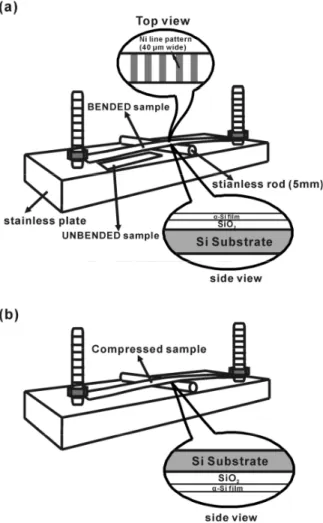
Features of the Bending Fixture
In this study, the tensile stress on the silicon film was introduced to the sample using a stainless bending fixture as shown in Fig. 2-2 (a). It is a simple equipment, without any vacuum or pumping system like the previous study.[2.4,2.5] The tensile stress was characterized by laser Raman spectroscopy on the basis of the extra shift of a Raman frequency. Since the Raman peak of α-Si was too broad and too weak to measure the difference, a single-crystal Si(100) sample was used to measure the peak shift. The Raman shift for a bended Si substrate (519.9 cm-1) was smaller than that for a stress-free Si substrate (520.437 cm-1). The stress in a bended Si substrate estimated from an extra peak shift was 241 MPa.[2.6] The actual stress, however, could not be determined because both the Si substrate and the Si film undergo plastic deformation at elevated temperatures. These samples were
33
designated as ‘‘BENDED’’. For the purpose of comparison, other samples were also annealed under the same conditions but without tensile stress. They were labeled as ‘‘UNBENDED’’. For the purpose of comparison, as shown in Fig. 2-2 (b), when the sample was turned upside down, a compressive stress was introduced to the Si film.
Fig. 2-2 Schematic illustration of stainless bending fixture, (a) BENDED (tensile) sample
and UNBENDED sample, and (b) compressed sample. The side view shows the sample structure and the top view the location of the Ni line pattern.
34
2-2-2
Preparation for the Bending Sample
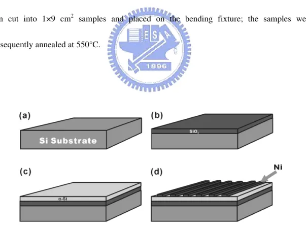
As shown in Fig. 2-3, silicon (100) wafers were used as the substrates in this study. Wet oxide films of 500 nm thickness were grown using a H2/O2 mixture at a substrate temperature
of 1050°C. Silane-based α-Si films with a thickness of 100 nm were then deposited using a low-pressure chemical vapor deposition (LPCVD) system at 550°C. The photoresist was then patterned to form the desired Ni features, and a 10-nm-thick Ni film was deposited on α-Si by the sputtering method. After samples were dipped into acetone and ultrasonic bath for 5 min, Ni deposited on the photoresist was removed together with the photoresist. The wafers were then cut into 1×9 cm2 samples and placed on the bending fixture; the samples were subsequently annealed at 550°C.
35
2-3
Results and Discussion
2-3-1
OM and SEM Analysis
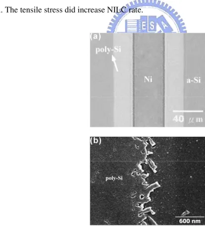
Figure 2-4 (a) shows the NILC poly-Si induced by 40-µm-wide Ni lines after 6 h of annealing. The light region at the periphery of the Ni lines was the poly-Si area. After dipping in the Secco solution,[2.7] the samples were examined by SEM. A typical SEM image of the NILC front region is shown in Fig. 2-4 (b). The morphologies of UNBENDED samples were similar to those of BENDED (tensile) samples. The only difference was that the NILC length of BENDED samples was 26 µm, which was longer than that of UNBENDED samples, 22 µm. The tensile stress did increase NILC rate.
Fig. 2-4 (a) Optical microscopy image of BENDED sample annealed at 550°C for 6 h. (b)
36
However, the NILC crystal length of BENDED samples was dependent on the position of Ni lines. As shown in Fig. 2-5, the NILC length was 26 µm for the Ni lines located at the center of the Si substrate, while it decreased to 22 µm for the Ni lines located near the edge of the Si substrate. This is because, with our stainless fixture, most of the bending force is applied on the center of the samples. Not much stress is applied near the edge of the Si substrate. Therefore, NILC length near the edge of the Si substrate did not increase.
Fig. 2-5 Illustration of the NILC growth length (BENDED sample) related to the position of
Ni lines.
The NILC length of BENDED samples was also dependent on the direction of the Ni lines. As shown in the Fig. 2-6, the induced NILC length of Ni lines parallel to the bending direction (26 µm) was longer than that of Ni lines perpendicular to the bending direction (22 µm), which was equal to the UNBENDED sample. This is because in the pure bending, the stress perpendicular to the bending direction is equal to zero.[2.8]
37
Fig. 2-6 Optical microscopy (OM) image of the NILC growth length (BENDED sample)
related to the direction between Ni line and bending direction.
2-3-2
A Series Two-Step for NILC
As mentioned previously, the NILC growth mechanism involved three stages. The enhancement of NILC length observed in our BENDED (tensile) samples might have resulted from two mechanisms: (1) reduction in NILC incubation time (included NiSi2 formation and
c-Si nucleation stages) and/or (2) increase in c-Si growth rate. In order to test the effects of tensile stress on those three stages of the NILC growth mechanisms, a series of two-step annealing processes were used in this work. The details of these processes are listed in Table I. Samples were first annealed under either an UNBENDED or a BENDED condition for 6 h. Each set of samples was then annealed again either in an UNBENDED or a BENDED condition for another 6 h. They were labeled as ‘‘UNBENDED–UNBENDED’’, ‘‘UNBENDED–BENDED’’, ‘‘BENDED–UNBENDED’’ and ‘‘BENDED–BENDED’’.
38
As shown in Table I, in the first UNBENDED annealing step, the NILC lengths of both UNBENDED–UNBENDED and UNBENDED–BENDED samples were the same. Then samples were annealed again under either an UNBENDED or a BENDED condition for another 6 h. In the second annealing step, the extra NILC length of the UNBENDED–BENDED sample was 26 µm, which was longer than that of the UNBENDED–UNBENDED sample (22 µm). In this annealing step, there was no need for NiSi2 formation and c-Si nucleation; NILC growth rate was only dependent on c-Si growth
rate. Therefore, the tensile stress in the second step must have increased c-Si growth rate, which increased NILC growth length.
However, in the second annealing step of BENDED–UNBENDED and BENDED–BENDED samples, the extra NILC lengths of both samples were the same, 22 µm. As described in the previous section, if there had been any tensile stress, c-Si growth rate should have increased. Thus, the absence of c-Si growth rate increase indicated that during the second BENDED annealing step, no tensile stress was applied on the BENDED–BENDED
39
sample. The decrease in tensile stress is not surprising since the yield stress of Si is only about 100 MPa at 550°C,[2.9] which is much less than the applied stress 241 MPa. The effective tensile stress on the Si film vanished due to plastic deformation. This plastic deformation was confirmed by the observation of the samples after the first BENDED annealing step as shown in Fig. 2-7. It means that the effective tensile stress in the second BENDED annealing step for BENDED–BENDED samples (applied using the bending fixture) on the Si film vanished.
Fig. 2-7 Photograph of bended sample annealed at 550°C for 6 h. The sample was bent due
to plastic deformation.
Figure 2-7 also shows that most of the plastic deformation occurred at the center of the Si substrate, and little deformation occurred at the edge of the substrate. That is, not much stress was applied near the edge of the Si substrate. This behavior is consistent with our previous
40
observation of various NILC lengths in different positions on the Si substrate. The induced NILC length near the edge of the bended Si substrate did not increase.
In order to study the effects of annealing time on the NILC growth mechanisms, the NILC lengths of the UNBENDED and BENDED samples are plotted as a function of annealing time in Fig. 2-8.
Fig. 2-8 NILC growth length as function of annealing time.
It was found that the lateral growth lengths of BENDED samples were always higher than those of UNBENDED samples. The NILC length difference between the BENDED and UNBENDED samples increased with annealing time. However, when the annealing time
41
However, the slope of the curve shown in Fig. 2-8 could be used to estimate NILC rate as a function of annealing time. It clearly shows that the growth rates (slope) of the UNBENDED and BENDED samples are the same when the annealing time exceeds 4 h. As mentioned previously, tensile stress would increase c-Si growth rate, and the effective tensile stress would vanish due to plastic deformation. These observations clearly showed that the effective tensile stress on the BENDED sample vanished when the annealing time exceeded 4 h.
2-3-3
Mechanism for the Effects of Tensile Stress on the
Growth of NILC
From this observation, the increase in c-Si growth rate caused by tensile stress is considered as follows. It has been reported that the growth of NILC is governed by the migration of NiSi2 precipitates through α-Si as illustrated in Fig. 2-9 (a),[2.2,2.10,2.11]
Hayzelden and Batstone[2.2] suggested that the driving force behind NILC is that the chemical potential of Ni is lower at the NiSi2/α-Si interface, whereas the chemical potential of
Si atoms is lower at the NiSi2/c-Si interface. In order to decrease free energy, the Ni atoms
should move toward a-Si and they in turn react with α-Si to form new NiSi2. The remaining Si
atoms attach to the NiSi2 template to form c-Si because their chemical potential is lower at the