國
立
交
通
大
學
電子工程學系 電子研究所
碩 士 論 文
三維積體電路的空白空間分散與熱相關功能區塊的放置
位置
White Space Distribution and Thermal-Aware 3D IC
Placement
研 究 生:蕭佳蕙
指導教授:陳宏明 教授
三維積體電路的空白空間分散與熱相關功能區塊的放置
位置
White Space Distribution and Thermal-Aware 3D IC
Placement
研 究 生:蕭佳蕙 Student:Chia-Hui Hsiao
指導教授:陳宏明 Advisor:Hung-Ming Chen
國 立 交 通 大 學
電子工程學系 電子研究所
碩 士 論 文
A ThesisSubmitted to Department of Electronics Engineering and Institute of Electronics
College of Electrical and Computer Engineering National Chiao Tung University
in partial Fulfillment of the Requirements for the Degree of
Master in
Electronics Engineering
September. 2010
Hsinchu, Taiwan, Republic of China
三維積體電路的空白空間分散與熱相關功能區塊的放置位
置
學生: 蕭佳蕙
指導教授: 陳宏明 教授
國立交通大學 電子工程學系 電子研究所 碩士班
摘
要
近年來,三維積體電路成為一個重要的趨勢,它帶來的好處有增加電路的效 能和減少繞線長度,但是相對的也帶來很嚴重的熱度問題。在這篇論文裡,提出 一個三維積體電路的熱相關功能區塊的放置位置演算法,藉由三維切割減少矽穿 孔的數量以及藉由三維積體電路的功能區塊的放置位置來最佳化繞線長度與熱 度。熱影響被結合在繞線的比例上,因此最小切割布局法可以考慮到熱。另外, 我們用了空白空間來散熱。在實驗結果顯示,我們的三維積體電路的熱相關功能 區塊的放置位置演算法可以減少 29%的最高溫度只需要增加 2%的繞線長度做為 代價。White Space Distribution and Thermal-Aware 3D IC
Placement
Student: Chia-Hui Hsiao Advisor: Prof. Hung-Ming Chen Department of Electronics Engineering
Institute of Electronics National Chiao Tung University
ABSTRACT
The 3D IC technologies can improve circuit performance and reduce wirelength. However, its thermal problems have become more serious. In this thesis, we propose a thermal aware 3D IC placement by using 3D partition to reduce the number of through-silicon via and to optimize wirelength and temperature. In our methods, thermal effect is integrated with the placement process by net weighting so that the min-cut in every partition process would reduce temperature. Furthermore, we distribute white space uniformly to dissipate heat. The experimental results show that our thermal aware 3D IC placement algorithm can reduce about 29% max temperature with only 2% increase on wirelength.
致謝
感謝許多人的幫助,讓我完成了這一篇論文。 首先,我要感謝我的指導教授陳宏明,在他的指導下讓我對自己研究的領域 有更深入的瞭解,建立了研究的興趣與自信心。陳宏明教授提供了一個非常優良 的研究環境與充足的研究資源,讓我能夠充分發揮自己的能力完成這一篇論文。 感謝實驗室的成員,在過去的兩年當中在生活上與研究上對我的幫助。感謝 研究室的所有學長姐對於我在研究上的幫忙,讓我解答疑難雜症。也要感謝陳奕 蓉同學,與我一路上互相鼓勵與成長。同時也感謝研究室的學弟妹,你們是相當 貼心的小朋友。 最後我要感謝我的家人對我在生活上的關心與幫助,讓我能夠順利的完成碩士的 論文研究。Contents
Abstract (Chinese) i Abstract ii Acknowledgements iii Contents iv List of Tables viList of Figures vii
1 Introduction 1
1.1 Motivation and Contributions . . . 1
1.2 Thesis Organization . . . 3
2 Preliminaries 4 2.1 Thermal-Aware 3D IC Placement Overview . . . 4
2.1.1 3D IC Placement . . . 4
2.1.2 Temperature Calculation . . . 5
3 Methodology 8
3.1 The Flow of Our Methodology . . . 8
3.2 Layer Assignment Considering Area Balance . . . 9
3.3 Thermal Model . . . 11
3.3.1 Heat Transfer Equation . . . 11
3.3.2 Finite Difference Method . . . 12
3.4 Partitioning-Based Placement Considering White Space Distribution . 15 3.4.1 Thermal-Aware Net-Weighting . . . 16
3.4.2 White Space Distribution . . . 18
3.5 Simulated Annealing Refinement . . . 19 4 Experimental Results 21 5 Conclusions and Future Works 24
List of Tables
3.1 Analogy of the equivalent thermal circuit . . . 14 3.2 Cooling Schedule α vs. T . . . 19 4.1 Characteristic of benchmark . . . 21 4.2 Experimental results comparing partitioning-based placement with
and without thermal . . . 22 4.3 Experimental results comparing placement with and without thermal 22
List of Figures
1.1 Wirelength reduction . . . 1
1.2 TSV in 3D . . . 2
1.3 High power density . . . 3
3.1 Our methodology flow chart . . . 9
3.2 Partition to layer . . . 10
3.3 Partition procedure . . . 11
3.4 Discretize 3D plane with ∆x, ∆y and ∆z in x, y and z coordination . 13 3.5 Thermal circuit . . . 14
3.6 Layer assignment and partitioning-based placement . . . 16
3.7 White space . . . 18
Chapter 1
Introduction
1.1
Motivation and Contributions
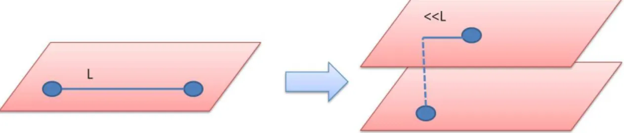
With the advencement of VLSI, three-dimensional integrated circuits have be-come an important technology which reduces interconnect delay and improves sys-tem performance [3]. Moreover, the shortened wirelength(Figure 1.1) can also reduce the power consumption of the circuit. To realize the 3D ICs’ potential, more and more design tools are developed.
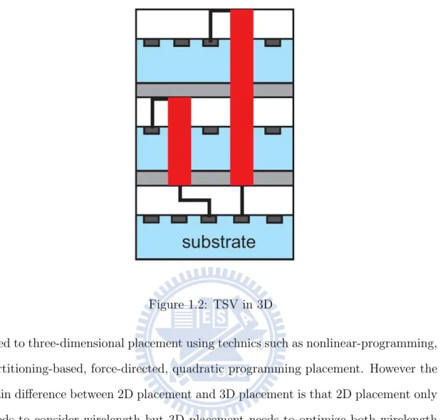
In 3D IC, through-silicon(TS) vias are used to connect device layers [2] (see Fig-ure 1.2). Typical size of TS vias ranges from 5um to 20um, which are much larger than wires, local vias, and cells. Therefore, a large number of TS via will affect overall chip area. So, we need to control the number of TS via in the circuit during physical design process. Recently, many two-dimensional (2D) placements are
Figure 1.2: TSV in 3D
plied to three-dimensional placement using technics such as nonlinear-programming, partitioning-based, force-directed, quadratic programming placement. However the main difference between 2D placement and 3D placement is that 2D placement only needs to consider wirelength but 3D placement needs to optimize both wirelength and TS via counts.
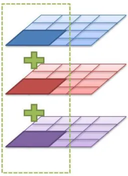
Because of high power densities(see Figure 1.3) and low thermal conductivities, one of the most critical issues of 3D IC design is thermal [1]. However, how to integrate thermal with placement process is a big problem. The reason is that precise thermal analysis such as finite element method (FEM) and finite difference method (FDM) take too much time. In fact, many placement algorithms are iterative processes. Thus, fast thermal calculation in placement process is the commonly used method.
In this thesis, we propose a thermal aware 3D IC placement through the fol-lowing procedure: 3D IC partition and 3D IC placement. For 3D IC partition, we
Figure 1.3: High power density
propose two-layer FM partition and multi-layer FM partition methods. As for 3D IC placement, it is composed of partitioning-based placement and simulated annealing refinement. Our contribution is that TS via numbers are minimized by 3D IC par-tition and thermal problem is integrated with placement process by net-weighting and white-space distribution.
1.2
Thesis Organization
The rest of this thesis is organized as follows. Chapter 2 introduces preliminaries about thermal aware 3D IC placement overview and problem formulation. Chapter 3 describes our methodology algorithm. Chapter 4 shows the experimental results and Chapter 5 presents the conclusions and future works.
Chapter 2
Preliminaries
2.1
Thermal-Aware 3D IC Placement Overview
2.1.1
3D IC Placement
Today, the general cell placement algorithms are quadratic placement, partitioning-based placement, force-directed placement and simulated annealing placement. Above algorithms are used by most of existing placers because of their performance. Many 3D cell placers exist in the literature. Most of 3D IC placement methods could be viewed as the extension of 2D placement techniques. We would introduce the 3D placement techniques as follows.
Partitioning-based approach would separate the region iteratively. The cost of the partitioning is measured by a weighted sum of the estimated wirelength and the TS via number. In [15], partitioning-based placement is divided into two procedures: layer assignment and partitioning-based placement in each layers. As [8] and [13], it merges the layer assignment and partitioning-based placement in layer process. And in [8], it adds thermal effects into net-weighting.
Quadratic placement approach and force-directed placement approach are devel-oped from analytical placement approach. The minimization of a quadratic objective function could be transformed to the function of linear system. In [7], it applies a
force-directed placement approach to decide the cell placement, and the tempera-ture is interpreted as thermal force. However, a 3D force-directed placement would place each cell in a true 3D space making z -position to be continuous value. So, rounding is needed for layer assignment. A quadratic programming approach [9] was also applied to the 3D context, which integrates thermal effect with a discrete cosine transformation base cost function.
Multilevel approach further applied to the analytical placement approach [10]. It adds the density penalty function into objective function and solves the placement problem from the coarsest level to the finest level. However, it does not consider thermal effects during placement process.
Despite above approach, in [6], it uses a 2D placement results and then uses folding/stacking based layer assignment. In this work, thermal is only considered during legalization process.
2.1.2
Temperature Calculation
Many methods have been used to calculate temperature results such as finite ele-ment analysis (FEA), finite-difference method (FDM), finite volume-based method, Fourier method, alternating direction implicit (ADI) method, and Green function method using discrete cosine transforms. Furthermore, some placements would use fast temperature calculation method during placement process. The temperature calculation methods are described as follows.
In [6], it uses compact resistive thermal network from CFD Research Corporation to calculate temperature. Compared with the accurate simulation tool, the error of this resistive network is smaller than 2%. It uses closed-form formula method during legalization to speed up.
and solve it by linear solver. It develops two fast but lack of accuracy temperature calculation methods to integrate temperature in the objective function. The first method makes use of thermal contribution of cells in a region and the second method updates the temperature in the same ratio as the power density ratio.
Finite Element Analysis (FEA) method was also applied to [7] and [8] to calculate temperature results. As [14], a 3D-ADI thermal simulator [5] is used to calculate temperature and it does not update temperature in every change because it is too expensive from runtime point of view.
2.2
Problem Formulation
Given a hypergraph H = (V, E), the placement region R, and the number device layer K, where V is the set of cells and E is the set of nets, a placement (xi, yi, zi) of
the cell satisfies that (xi, yi) ∈ R and zi ∈ {1, 2, ..., K}. The task of thermal-aware
3D placement problem is to assign a position (xi, yi, zi) to every cell vi, so that the
total wirelength, the TS via numbers and the temperature are minimized.
To optimize thermal during placement process, we define the objective function which is a weighted sum of the total wirelength and TS via number, cell temperature.
OBJ =X
e∈E
(W L(e) + αT SVT SV (e)) + αtemp
X
vi∈V
T (2.1) where W L(e) is the bounding box wirelength and T SV (e) is the number of the TS via number for net e, Ti is the temperature of the cell i, αT SV is the TS via coefficient
and αtemp is the thermal coefficient.
We use traditional half-perimeter model for wirelength calculation and project all cells to 2D plane, where the wirelength W L(e) of a net e is calculated as follows:
W L(e) = (max vi∈e {xi} − min vi∈e {xi}) + (max vi∈e {yi} − min vi∈e {yi}) (2.2)
We also estimate TSV number through similar model. The TS via number
T SV (e) is calculated as follows:
T SV (e) = (max
vi∈e
{zi} − min vi∈e
Chapter 3
Methodology
In this chapter, we propose a 3D IC placement considering thermal and white-space distribution. The organization of this chapter is described as follows. First, we introduce the flow of our methodology in Section 3.1. Second, in Section 3.2, we describe layer assignment considering area balance which includes TS via area. Then, the thermal model in this thesis is shown in Section 3.3. In Section 3.4, a partitioning-based 3D IC placement considering thermal and white-space distribu-tion is implemented. Finally, the simulated annealing refinement method is pre-sented in section 3.5.
3.1
The Flow of Our Methodology
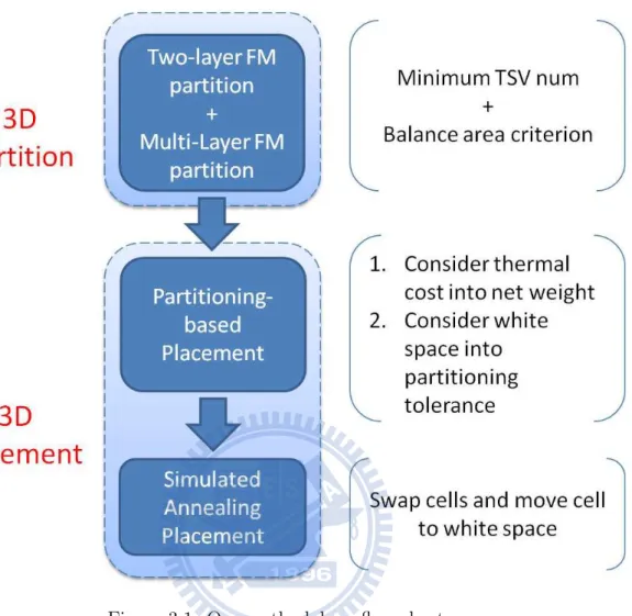
The whole methodology flow is shown in Figure 3.1. A 3D IC partition is first used to distribute cells to different layers. The goal of 3D IC partition is to minimize the connections between layers and consider area balance in every layer at the same time. Then, a 3D IC placement is used to produce placement results. Partitioning-based placement is the main technique of 3D IC placement, and then it uses a simulated annealing to refine the placement result. During partitioning-based placement, it would consider thermal effects during min-cut and the partition would terminate if it cannot satisfy partition tolerance. A simulated annealing refinement
Figure 3.1: Our methodology flow chart
process would reduce wirelength by iteration. Finally, we would get the placement result for each device layer.
3.2
Layer Assignment Considering Area Balance
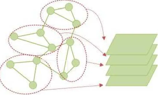
The partitioning-into-layers step is performed using multi-layer FM partition together with two-layer FM partition and the illustration shows in Figure 3.2. The goal of partitioning-to-layers is to minimize the TS via number.
Two-layer FM partition is the traditional FM partition implemented. It executes FM partition in two layers so that cells can only move between two layers. The goal
Figure 3.2: Partition to layer
of two-layer FM partition is to generate a min-cut partition in two layers under area balance constraint.
We develop a new multi-layer FM partition which is modified from traditional two-layer FM partition. It would consider more than two layers during FM parti-tion. When we execute two-layer FM partition, it would generate a good min-cut partition result in only two layers, but the total TS via number may get worse while considering whole layers and it would take too much time during iteration. There-fore, we change two layers into whole layers. In this way, cells can move between three layers which include this layer, upper layer and down layer. As a result, we divide the gain of the cell into move up gain and move down gain. So, it is more efficient to use multi-layer FM partition than two-layer FM partition.
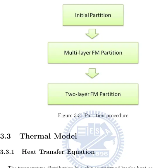
The procedure is shown in Figure 3.3. The flow of layer assignment starts from initial partition which assigns cells to different layers in distribution, and then multi-layer FM partition is implemented to minimize TSV number. At last, we use two-layer FM partition iteratively to further minimize TSV number.
Figure 3.3: Partition procedure
3.3
Thermal Model
3.3.1
Heat Transfer Equation
The temperature distribution in a chip is governed by the heat conduction equa-tion:
ρCρ
∂T (~r, t)
∂t = ∇[κ(~r, T )∇T (~r, t)] + g(~r, t) (3.1)
where ρ is the density of the material, Cρis the specific heat of the material, κ is the
thermal conductivity of the material, T is the temperature, and g is the heat gener-ation rate. This equgener-ation is derived from the law of energy conservgener-ation. ρCρ∂T∂tdV
is the rate of energy causing the temperature increase,R κ∇T dA =R ∇[κ∇T ]dV is
the rate of heat flow entering the volume,andR gdV is power generated in volume.
If we model packaging, heat sinks, and cooling systems as 1-D equivalent thermal resistance, the equivalent boundary condition is:
κ(~r, T )∂T (~r, t)
where he
i = 1/AiRiθ is the heat transfer coefficient in the direction of heat flow i
,fi is an arbitrary function on the boundary surface, Ai is the effective area normal
to ~i and Ri
θ is the equivalent thermal resistance.
3.3.2
Finite Difference Method
In this work, we use the thermal model proposed in [4]. In homogeneous material, the heat transfer equation can be obtained by
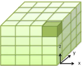
ρCρ ∂T (~r, t) ∂t = κ[ ∂2(~r, t) ∂x2 + ∂2(~r, t) ∂y2 + ∂2(~r, t) ∂z2 ] + g(~r, t) (3.3)
This equation can be discretized with size ∆x, ∆y and ∆z in x, y and z di-rection(see Figure 3.4 ). Then the temperature T (x, y, z, t) at node (i, j, k) can be replaced by T (i∆x, j∆y, k∆z, t) , which is denoted as Ti,j,k for the rest of the
thesis. Using central-difference equation, the difference equation at node(i,j,k) can be expressed as ρCρ∆V dTi,j,k dt = −κ Ax ∆x(Ti,j,k− Ti−1,j,k) −κAx ∆x(Ti,j,k− Ti+1,j,k) −κAy
∆y(Ti,j,k− Ti,j−1,k)
−κAy
∆y(Ti,j,k− Ti,j+1,k)
−κAz
∆z(Ti,j,k − Ti,j,k−1)
−κAz
∆z(Ti,j,k − Ti,j,k+1)
+∆V gi,j,k (3.4)
where ∆V = ∆x∆y∆z is the volume of the node(i,j,k), ∆V g is the total power generated within the element, Ax = ∆y∆z, Ay = ∆x∆z, Az = ∆x∆y.
Figure 3.4: Discretize 3D plane with ∆x, ∆y and ∆z in x, y and z coordination
The equation can further be translated into the equivalent lumped thermal circuit as shown in Figure 3.5: CθdTi,j,k dt + Ti−1,j,k− Ti,j,k Rθ i−1,j,k +Ti+1,j,k − Ti,j,k Rθ i+1,j,k +Ti,j−1,k− Ti,j,k Rθ i,j−1,k + Ti,j+1,k− Ti,j,k Rθ i,j+1,k + Ti,j,k−1− Ti,j,k Rθ i,j,k−1 +Ti,j,k+1− Ti,j,k Rθ i,j,k+1 = Qp (3.5)
where Cθ = ρC∆V is the thermal capacitance, ∆V g is the heat flow from power
generated in ∆V , and Rθ
i±1,j,k = κA∆xx, R
θ
i,j±1,k = κA∆yy, and R
θ
i,j,k±1= κA∆zz are the
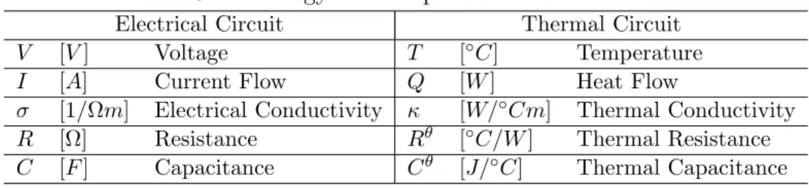
ther-mal resistances. In isotherther-mal boundary condition, the nodes which are connected to the ambient correspond to the ground node. The analogy between electrical and thermal circuits is shown in Table 4.1. In fact, this equation is equivalent to the KCL in electrical circuit at node (i, j, k) because heat flow equals to current flow in electrical circuits.
From the above equation, we can construct the thermal circuit. First we decide the grid size and then resistance and heat flow also present. After mapping thermal circuit into electrical circuit, we solve the lumped thermal circuit by SPICE. Finally we get the temperature of each node.
Figure 3.5: Thermal circuit
Table 3.1: Analogy of the equivalent thermal circuit
Electrical Circuit Thermal Circuit
V [V ] Voltage T [◦C] Temperature
I [A] Current Flow Q [W ] Heat Flow
σ [1/Ωm] Electrical Conductivity κ [W/◦Cm] Thermal Conductivity
R [Ω] Resistance Rθ [◦C/W ] Thermal Resistance
3.4
Partitioning-Based Placement Considering White
Space Distribution
The following algorithm describes partitioning-base 3D IC placement process: Partitioning-based 3D IC Placement
1. for all layers i = 0 to L-1
2. do partitioning-based placement of layer i 3. while quene not empty
4. do dequene a block
5. if satisfy the partition tolerance 6. than bipartition into smaller block 7. enquene each block
8. else the block is finished
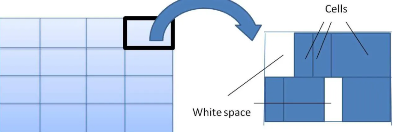
After layer assignment, partitioning-based placement is performed on each layer. The placement of each layer is based-on recursive bisection using Patoh [17] par-titioning algorithm. The goal of this stage is to minimize wirelength and thermal effects. When a region is partitioned, two new regions are created from the par-titioned cells and the divided areas. For each partition process, we use terminal propagation [18] to consider the connectivity outside the region so that the wire-length would not be too large. In the fixed-die placement constraint, the white space is given before placement. Therefore, we distribute white-space in every small re-gion to dissipate heat. In Figure 3.6, after layer assignment and partitioning-based placement, the placement is divided into many small regions. In a small region only few cells are there.
Figure 3.6: Layer assignment and partitioning-based placement
3.4.1
Thermal-Aware Net-Weighting
In order to add thermal effects to partitioning-based placement, we use net-weighting technique [8]. It would consider the power and thermal resistance used in each net. Originally, the objective function with thermal consideration is represented as
OBJ =X
e∈E
(W L(e) + αT SVT SV (e)) + αtemp
X
vi∈V
T (3.6) However, Ti can be replaced by ∆Ti which is the temperature change of cell i.
And ∆Ti can be calculated by fast calculation during placement process:
∆Ti = Pi∗ Ri (3.7)
where Pi is the power dissipation of cell i, and Ri is the thermal resistance of cell i.
Therefore, the objective function becomes:
OBJ = X
e∈E
(W L(e) + αT SVT SV (e)) + αtemp
X
vi∈V
∆T = X
e∈E
(W L(e) + αT SVT SV (e)) + αtemp
X
vi∈V
RiPi (3.8)
In this stage, the thermal resistance of cell i is calculated as:
Ri = (Rlef t,i−1 + R−1right,i+ R−1rear,i+ R−1f ront,i+ Rbottom,i−1 + R−1top,i)−1 (3.9)
where R−1
lef t,i, R−1right,i, R−1rear,i, R−1f ront,i, R−1bottom,i, R−1top,i are calculated by simplify finite
the cell to the chip surface in all three directions and that the cross sectional area of a path is equal to the same size as the cell. We also assume that total power is dominated by dynamic power. Therefore, the power dissipation of cell i is
Pi =
X
netedrivenbyvi
0.5aef VDD2 (CperW LW L(e) + CperT SVT SV (e) + Cperpinninputpinse )
(3.10) where ai is the switching activity, f is the clock frequency, VDD is the power supply,
CperT SV is the capacitance per wirelength, CperT SV is the capacitance per TSV,
Cperpin is input pin capacitance, and ne is the number of the cell input pins attached
to net i.
By dropping the terms Cperpinninputpinse and replacing CperT SV by CperW LαT SV,
the objective function can be expressed as
OBJ =X
e∈E
(1 + αtemp∗
X
cellvidrivingnete
Ri∗ 0.5aef VDD2 CperW L)(W L(e) + αT SVT SV (e))
(3.11) The general weighted wirelength objective function of 3D IC placement can be expressed as
OBJ =X
e∈E
(1 + re)(W L(e) + αT SVT SV (e)) (3.12)
From the above two equation, we can obtain the net weighting is
re= αtemp∗
X
cellvidrivingnete
Ri∗ 0.5aef VDD2 CperW L (3.13)
Therefore, in every partition process, we should minimize the weighted cut size P
Figure 3.7: White space
3.4.2
White Space Distribution
After we convert the benchmark from 2D to 3D, we should decide the area of a layer. If we set the layer area the same as the 2D benchmark, the performance would be very bad because the cells may spread out the whole chip. In our work, the benchmarks are integrated with four layers. The placement area is scaled by dividing the original area by 4, and then enlarging it to obtain more white space.
In fixed-die constraint, the chip area, core area, rows and available sites are given before design [20]. Therefore, we have white space now. So using white space to increase heat dissipation is a method to solve thermal problem [21]. However, the fixed-die style does not change the placement method but make problems. For example, in fixed-die placement, purely minimizing wirelength tends to place all the cells close to each other, but the congestion of this design tends to make heat dissipation worse. Therefore, it would be a trade-off between providing white space for heat dissipation and wirelength reduction.
In this work, we assign white-space in distribution so that in every small region could have space to dissipate heat. Figure 3.7 shows the white space preserved for heat dissipation. It ensures that white space would not compact on one region.
Table 3.2: Cooling Schedule α vs. T For T≥ α 40000 0.8 20000 0.84 10000 0.88 5000 0.91 200 0.94 100 0.9 50 0.85 5 0.8 1.5 0.7 0 0.1
However, we should consider the situation that the cells would be distributed in chip everywhere making the wirelength worse. As a result, we should just preserve the white space which we need in a small region.
We calculate the white space in the small region as a percentage. After partitioning-based placement, in every small region we would perserve nearly the same percent-age. Therefore, it would not cause the situation that the white space is located in only one region.
Thus, using the above techniques including net weighting and white space dis-tribution, we can obtain the placement result with thermal considerations.
3.5
Simulated Annealing Refinement
In this stage, we use simulated annealing refinement to further reduce wirelength. We use swapping a pair of cells and displacement of a single cell to white space to realize simulated annealing. Wirelength could be minimized by a long run time.
For simulated annealing, the cooling schedule strongly affects the quality of the final placement. In this work, we use Timberwolf [19] cooling schedule. The update
of temperature is given as:
Tnew = α(Told) ∗ Told 0 < α < 1 (3.14)
The variable α is shown in Table 4.2. In this way, for T ≥ 40000, α is set to 0.8, for 40000 > T ≥ 20000, is set to 0.84, and so on. Using this cooling schedule, temperature is reduced iteratively until T < 0.1. We can find the global optimal solution when we adopt this cooling schedule. Therefore, we can obtain the final placement result by iteration.
Chapter 4
Experimental Results
Our algorithms were implemented in C++/STL, compiled with gcc v4.1.2 and run on Intel 5160 1998 MHz workstation.
We test the algorithm on IBM-place 2.0 benchmarks [22] for standard cells, and the characteristic of the benchmarks is present is Table 4.1 with the number of cells, the number of nets. Because only these testcases are transformed to lef and def file, we only test our algorithm on these testcases. In our work, the benchmarks are integrated with four layers for all test cases. The placement area is scaled by dividing the original area by 4, and then enlarging it to obtain white space. The grid size is set to 20 × 20 × 4. The substrate thickness was set to 500um, the layer thickness is set to 5.7um, and the interlayer thickness was set to 0.7um.
The thermal conductivity of the silicon in the chip substrate was set to 10.2W/m∗
K. The power dissipation of each cell was calculated by multiplying its area by a
random value range from 0 to 2 × 10⁷W/m2. The top and sides of the chip were
Table 4.1: Characteristic of benchmark
circuits cells nets
ibm01 12028 11753 ibm02 19062 18688 ibm07 44811 44681 ibm08 50672 48230
Table 4.2: Experimental results comparing partitioning-based placement with and without thermal
circuits Partitioning-based Placement Partitioning-based Thermal-aware Placement WL TSV number CPU WL TSV number CPU
ibm01 94.8 3222 16.4 114.7 3222 16.9 ibm02 240.7 1212 48.6 255.0 1212 50 ibm07 507.4 19202 152.9 524.2 19202 155.9 ibm08 505.0 22199 261.6 620.2 22199 265.8 avg 1 1 1 1.12 1 1.01
Table 4.3: Experimental results comparing placement with and without thermal
circuits Placement without thermal Thermal aware placement WL TSV number Tmax CPU WL TSV number Tmax CPU ibm01 58.4 3222 58 21 58.9 3222 56 21 ibm02 157.7 1212 108 34 163.1 1212 76 34 ibm07 319.1 19202 90 92 326.8 19202 57 92 ibm08 339.0 22199 122 162 346.7 22199 81 162
avg 1 1 1 1 1.02 1 0.71 1
made adiabatic, and the bottom of the chip was made isothermal with ambient temperature. The ambient was set to 0◦C for convenience, but the temperature can
be translated by the amount of any ambient to reflect a different temperature. In Table 4.2, we compared the results of non-thermal partitioning-based 3D placement with thermal aware 3D placment. The unit of the CPU time is second. There is 12% increase in wirelength and 1% longer in CPU time. From the experi-mental result, we can see that we only take little time to calculate temperature.
Next, we compared the results of non-thermal 3D placement with thermal aware 3D placement in Table 4.3. The unit of the CPU time is minute. There is 29% reduction in average temperature, but there is only 2% increase in wirelength. In this work, the run time of non-thermal 3D placement and thermal aware 3D placement are nearly the same. The reason is that the simulated anneealing placement takes too much time so that the time of temperature calculation is few.
Figure 4.1: Run time analysis
At last, in Figure 4.1, the run time analysis shows that when the cells size increase it would take more time to execute. Because we use simulated annealing as the refinement, the CPU time would increase extremely.
Chapter 5
Conclusions and Future Works
In this thesis, we propose a 3D IC placement with thermal considerations. We first performed a 3D IC partition with a two-layer FM partition together with a multi-layer FM partition. We then performed a thermal-aware 3D IC placement by based placement and simulated annealing refinement. In partitioning-based placement, we use net-weighting and white-space distribution to consider heat dissipation. We obtained trade-off among temperature, wirelength, and via costs. The experimental results show the algorithm can obtain a reduction in the temperature with little wirelength increase.
For the future work on thermal placement, the power analysis should be more accurate, which have heavy impact on heat dissipation. Thermal via insertion would be a good method to solve 3D thermal problem and many works have already focus on it. Therefore, considering thermal via during 3D IC placement would be a task to work on.
Bibliography
[1] J. Cong, “An Automated Design Flow for 3D Microarchitecture Evaluation,”
Proceedings of the Asia and South Pacific Design Automation Conference,
pp. 384 - 389, 2006.
[2] W. R. Davis, J. Wilson, S. Mick, J. Xu, H. Hua, C. Mineo, A. M. Sule, M. Steer, and P. D.Franzon, “Demystifying 3D ICs: The pros and cons of going vertical,” Design & Test of Computers, vol. 22, pp. 498 - 510, 2005.
[3] Charles Chiang and Subarna Sinha, “The Road to 3D EDA Tool Readiness,”
Proceedings of the Asia and South Pacific Design Automation Conference,
pp. 429 - 436, 2009.
[4] T.-Y. Wang and C.-C. Chen, “Spice-compatible Simulation with Lumped Circuit Modeling for Thermal Reliability Analysis based on MOR,”
Proceed-ings of the International Symposium on Quality Electronic Design, pp. 357
- 362, 2004.
[5] T.-Y. Wang and C. C.-P. Chen, “A linear-time chip level transient thermal simulator,” IEEE Trans. on Computer-Aided Design of Integrated Circuits
and Systems, vol. 21, pp. 1434 - 1445, 2002.
[6] J. Cong, G. Luo, J. Wei, and Y. Zhang, “Thermal-aware 3d ic placement via transformation,” Proceedings of the Asia and South Pacific Design
[7] B. Goplen and S. S. Sapatnekar, “Efficient Thermal Placement of Stan-dard Cells in 3D ICs using a Force Directed Approach,” Proceedings of the
IEEE/ACM international conference on Computer-aided design, pp. 86 - 89,
2003.
[8] B. Goplen and S. Sapatnekar, “Placement of 3d ics with thermal and inter-layer via considerations,” Proceedings of the Design Automation Conference, pp. 626 - 631, 2007.
[9] H. Yan, Q. Zhou, and X. Hong, “Thermal Aware Placement in 3D ICs Using Quadratic Uniformity Modeling Approach,” Integration, the VLSI Journal, vol. 42, no.2, pp. 175 - 180, 2009.
[10] J. Cong and G. Luo, “A multilevel analytical placement for 3D Ics,”
Proceed-ings of the IEEE/ACM international conference on Computer-aided design,
pp. 361 - 366, 2009.
[11] B. Goplen and S. Sapatnekar, “Thermal Via Placement in 3D Ics,”
Pro-ceedings of the international symposium on Physical design, pp. 167 - 174,
2005.
[12] H. Yan, Q. Zhou, and X. Hong, “Efficient Thermal Aware Placement Ap-proach Integrated with 3D DCT Placement Algorithm,” Proceedings of the
International Symposium on Quality Electronic Design, pp. 289 - 292, 2008.
[13] S. Das, A. Chandrakasan, and R. Reif, “Design Tools for 3-D Integrated Circuits,” Proceedings of the Asia and South Pacific Design Automation
Conference, pp. 53 - 56, 2003.
[14] K. Balakrishnan, V. Nanda, S. Easwar, and S. K. Lim, “Wire congestion and thermal aware 3-D global placement,” Proceedings of the Asia and South
[15] C. Ababei, H. Mogal, and K. Bazargan, “Three-Dimensional Place and Route for FPGAs,” Proceedings of the Asia and South Pacific Design
Au-tomation Conference, pp. 773 - 778, 2005.
[16] D. H. Kim, K. Athikulwongse, and S. K. Lim, “A Study of Through-Silicon-Via Impact on the 3-D Stacked IC Layout,” Proceedings of the IEEE/ACM
international conference on Computer-aided design, pp.674 - 680, Nov. 2009.
[17] U. V. Catalyurek and C. Aykanat, “Hypergraph-partitioning based decom-position for parallel sparse-matrix vector multiplication,” IEEE Transactions
on Parallel and Distributed Systems, vol. 21, pp.673 - 693, 1999.
[18] A. E. Dunlop and B. W. Kernighan, “A Procedure for Placement of Standard Cell VLSI Circuits,” IEEE Trans. on Computer-Aided Design of Integrated
Circuits and Systems, vol. 1, pp.92 - 98, 1985.
[19] C. Sechen and A. Sangiovanni-Vincentelli, “TimberWolf3.2: A New Stan-dard Cell Placement and Global Routing Package,” Proceedings of the Design
Automation Conference, pp.432 - 439, 1986.
[20] X. Yang, B.-K. Choi, and M. Sarrafzadeh, “Routability driven white space allocation for fixed-die standard cell placement,” Proceedings of the
interna-tional symposium on Physical design, pp. 42 - 47, 2002.
[21] Linfu Xiao, Subarna Sinha, Jingyu Xu and Evangeline F.Y. Young, “Fixed-outline thermal-aware 3D floorplanning,” Proceedings of the Asia and South
Pacific Design Automation Conference, pp. 561 - 567, 2010.