具有副閘極結構之雷射退火複晶矽薄膜電晶體製作與特性研究
74
0
0
全文
(2) 具有副閘極結構之雷射退火複晶矽薄膜電晶體 製作與特性研究 The Fabrication and Characterization of Laser-Annealed Polysilicon Thin-Film Transistors with Sub-Gate Structures. 研 究 生:葉冠華. Student:Kuan-Hwa Yeh. 指導教授:張國明 博士. Advisor:Dr. Kow-Ming Chang. 國. 立. 交. 電子工程學系 碩. 通. 大. 學. 電子研究所碩士班 士. 論. 文. A Thesis Submitted to Institute of Electronics College of Electrical Engineering and Computer Science National Chiao Tung University In Partial Fulfillment of the Requirements for the Degree of Master In Electronics Engneering June 2004 Hsinchu, Taiwan, Republic of China. 中華民國九十三年六月.
(3) 具有副閘極結構之雷射退火複晶矽薄膜電晶體 製作與特性研究 研究生:葉冠華. 指導教授:張國明 博士. 國立交通大學 電子工程學系. 電子研究所碩士班. 摘. 要. 複晶矽薄膜電晶體已經廣泛的使用在液晶顯示器的畫素控制元件。而為了達 到將週邊驅動電路與畫素控制元件整合在同一大面積玻璃基板的目標,低溫多晶 矽的技術是重要關鍵。其必須具備高的驅動電流、低的漏電流,以及良好的可靠 度三個條件。不同的元件結構、結晶方法將影響元件特性甚巨。本論文結合了準 分子雷射退火結晶方法與兩種不同的副閘極元件結構,進行低溫多晶矽薄膜電晶 體的製作與特性研究,並且在不增加多餘光罩的前提下,加入新的製程步驟,以 求得到優異的元件特性。 由掃描式電子顯微鏡的照片可以觀察到結晶的晶粒大小約 1 μm,但是分佈 並不均勻,這是因為準分子雷射系統掃描均勻度不佳。因此經由準分子雷射結晶 製作的薄膜電晶體元件特性變異很大。 第一種副閘極結構在汲極/源極附近有自我對準厚閘極氧化層,可以降低漏 電流至少一個等級。為了改善因氧化層增厚而下降的導通電流,我們引入氮化矽 作為增厚層,雖然導通電流因為介電常數較大而提升,但是漏電流因為介面特性 差也較大,使得開關電流比與使用氧化層相近。最後我們將元件結構搭配ONO 堆疊式介電層得到了最佳的特性,在汲極電壓為 1 伏、閘極電壓為-5 伏時,漏電.
(4) 流為 2.25×10⁻¹⁰安培,比傳統低溫多晶矽薄膜電晶體改善了一百倍,且開關電流 比提升到 8.44×10⁷。具有副閘極結構的薄膜電晶體在靜態熱電子應力測試下,更 具有較少的最大轉導衰退以及臨限電壓偏移量。 第二種是具有副閘極耦合的元件結構,製造步驟完全與傳統薄膜電晶體相 同,藉由改變覆蓋面積比例R,具有與位移結構相似的電性。本論文中的最佳條 件是R=5,其在汲極電壓為 1 伏、閘極電壓為-5 伏時,漏電流為 3.51×10⁻¹⁰安培, 比傳統低溫多晶矽薄膜電晶體改善了一百倍,且開關電流比提升到 2.12×10⁷。為 了改善雷射退火造成多晶矽薄膜表面的粗糙度,在雷射退火結晶後的多晶矽上覆 蓋一層超薄非晶矽,搭配本結構得到了最佳特性。當此副閘極結構(R=5)覆蓋 5 nm超薄非晶矽且汲極電壓為 1 伏、閘極電壓為-5 伏時,漏電流為 2.4×10⁻⁹安培, 開關電流比為 5.85×10⁶。具有副閘極結構的薄膜電晶體在靜態熱電子應力測試 下,更具有較少的最大轉導衰退以及臨限電壓偏移量。.
(5) The Fabrication and Characterization of Laser-Annealed Polysilison Thin-Film Transistors with Sub-Gate Structures Student:Kuan-Hwa Yeh. Advisor:Dr. Kow-Ming Chang. Department of Electronics Engineering And Institute of Electronics National Chiao Tung University. ABSTRACT. Polycrystalline silicon thin-film transistors have been used widely in the pixel controller devices of active matrix liquid crystal displays(AMLCDs). The low temperature process of poly-Si TFTs is the key to integrate the peripheral driving circuits and pixel controller devices on the same large area glass substrate. It needs high driving current, low off-state leakage current, and good reliability. The electrical characteristics of poly-Si TFTs differ from various crystallization methods. In this thesis, we fabricate two kinds of sub-gate structure poly-Si TFTs by utilizing excimer laser annealing crystallization method and improve device characteristics without additional photo-masking steps. The average grain size is about 1~1.5μm in SEM graphs but the grain distribution is not uniform due to the laser beam irregularity. Thus, the variations among the poly-Si TFTs are notable. First sub-gate structure with a self-aligned thicker sub-gate oxide near the drain/source regions has leakage current lower on order than those of the conventional one. For the sake of larger driving current, we introduce the silicon nitride to the.
(6) thicker layer. Although the on-state driving current increased, the on/off current ratio is nearly unchanged due to higher leakage current. Finally, the sub-gate structure TFT with ONO stack gate dielectric shows the excellent properties. It shows the leakage current 100 times lower than those of the conventional ones and also shows on/off current ratio of 8.44×10⁷ at VGS=-5 V and VDS=1 V. The degradation of the maximum transconductance and the threshold voltage variations under static hot-carrier stress of sub-gate structure is also less than conventional one. Second floating sub-gate structure behaves as an offset gated structure by modulating overlapping area ratio R, and its fabrication processes is fully the same as the conventional TFT. The optimum condition is R=5 in this thesis. It shows the leakage current is 3.51×10⁻¹⁰ A and is 100 times lower than those of the conventional ones at VGS=-5 V and VDS=1 V. It also shows on/off current ratio of 2.12×10⁷ at VGS=-5 V and VDS=1 V. In order to improve the surface roughness of poly-Si film, we cap an ultra-thin a-Si layer on the laser-annealed poly-Si film. And it show better electrical characteristics. The sub-gate structure(R=5)TFT with a 5 nm-thick a-Si capping layer shows the low leakage current of 2.4×10⁻⁹ A and on/off current ratio of 5.85 × 10⁶ at VGS=-5 V and VDS=1 V. The degradation of the maximum transconductance and the threshold voltage variations under static hot-carrier stress of sub-gate structure is also less than conventional one..
(7) Contents Abstract(Chinese)………………………………………………………………i Abstract(English)……………………………………………………………..iii Contents...……………………………………………………………………..vii Table Lists…………………………………………………………………...….x Figure Captions……………………………………………………………...…xi. Chapter 1. Introduction. 1.1 An Overview of Low Temperature Polycrystalline Silicon(LTPS) TFTs………..1 1.2 Recrystallization of Amorphous Si(a-Si)Thin Films……………………………..2 1.2.1Solid Phase Crystallization…………………………………………………...3 1.2.2 Metal-Induced Lateral Crystallization ………………………………………3 1.2.3 Excimer Laser Annealing Crystallization……………………………………4 1.3 Low Temperature Deposition of Gate Dielectric……………………………….....4 1.4 Several Novel High Performance Structures for LTPS TFTs……………………...5 1.5 Motivation…………………………………………………………………………6 1.6 Thesis Organization………………………………………………………………..6. Chapter 2. Fabrication and Characterization of Low-Temperature Poly-Si TFTs. 2.1 Typical Polysilicon TFT Fabrication Flow………………………………………...8 2.2 Excimer Laser System……………………………………………………………..9 2.3 Methods of Device Parameter Extraction………………………………………....9 2.3.1 Determination of Threshold Voltage………………………………………...9 2.3.2 Determination of Subthreshold Swing……………………………………..10 2.3.3 Determination of Field Effect Mobility…………………………………….10.
(8) 2.3.4 Determination of On/Off Current Ratio……………………………………10 2.4 Reliability Issue…………………………………………………………………..11. Chapter 3. Poly-Si TFT with a Poly-Si Spacer Sub-Gate Structure. 3.1 Device Architectures……………………………………………………………..12 3.2 Process Flow……………………………………………………………………..12 3.3 Analysis of Grain Size by Scanning Electron Microscope(SEM)………………13 3.3.1 Sample Preparation………………………………………………………...13 3.3.2 SEM Graph Analysis and Discussion………………………………...…….14 3.4 The Characteristics of LTPS TFTs ………………………………………………14 3.4.1 Laser-Annealed Poly-Si TFTs with Poly-Si Spacer Sub-Gate Structures….14 3.4.2 Laser-Annealed Poly-Si TFTs with Thicker Sub-Gate Nitride………….…15 3.5 High Performance Sub-gate Structure TFTs with a Novel ONO Stack Gate Dielectric………………………………………………………………………….16 3.6 Reliability Issues…………………………………………………………………17 3.7 Summary…………………………………………………………………………18. Chapter 4. Laser-Annealed Poly-Si TFT with a Floating Sub-Gate Structure. 4.1 Device Architectures……………………………………………………………..19 4.2 Process flow…………………………………………………………………..….19 4.3 Electrical Properties and Characteristics…………………………………………20 4.4 Improving the Characteristics of Low-Temperature Poly-Si TFTs by an Additional Amorphous Silicon Interfacial Layer…………………………………………….22 4.5 Reliability Issues………………………………………………………………....24 4.6 Summary…………………………………………………………………………24.
(9) Chapter 5. Conclusions and Future Works. 5.1 Conclusions………………………………………………………………………26 5.2 Future Works……………………………………………………………………..27.
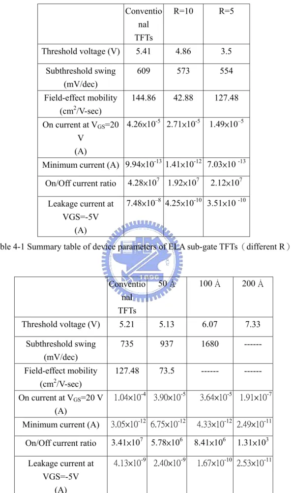
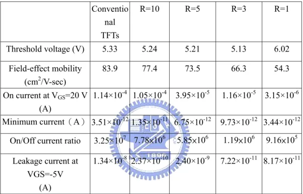
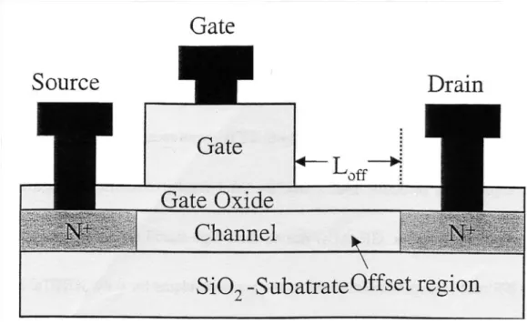
(10) Table Lists Chapter 2 Table 2-1 Process parameters in conventional TFTs. Table 2-2 Stress condition.. Chapter 3 Table 3-1(a) Process conditions of amorphous silicon deposited by LPCVD system. Table 3-1(b) Process conditions of polysilicon deposited by LPCVD system. Table 3-1(c) Process conditions of polysilicon dry etching by RIE system. Table 3-1(d) Process conditions of TEOS oxide(gate oxide)deposited by PECVD system. Table 3-2 The ONO stacked gate dielectric grown parameters Table 3-3 Statistical data of the electrical characteristics of LTPS TFT fabricated by different crystallization manners. Five TFTs were measured in each case. Table 3-4 Summary table of device parameters of all kinds of spacer sub-gate poly-Si TFTs. Chapter 4 Table 4-1 Summary table of device parameters of ELA sub-gate TFTs(different R) Table 4-2 Summary table of ELA sub-gate TFTs(R5)with different a-Si thickness. Table 4-3 Summary table of ELA + 50Å a-Si sub-gate(different R)TFTs..
(11) Figure Captions Chapter 1 Fig. 1-1 Offset TFT structure. Fig.1-2 LDD TFT structure.. Chapter 2 Fig. 2-1 Conventional TFTs cross-section view. Fig. 2-2 The schematic diagram of the sub-gate structure TFT.. Chapter 3 Fig. 3-1 The schematic diagram of the poly-Si spacer sub-gate structure. Fig. 3-2 The top view of the poly-Si spacer sub-gate structure. Fig. 3-3(a) The cross-section view along the line AA’. Fig. 3-3(b) The cross-section view along the line BB’. Fig. 3-4(a)-(f) Process flow of fabricating poly-Si spacer sub-gate structure TFT Fig. 3-5(a) the SEM image of poly-Si film crystallized by SPC after Secco-etch. Fig. 3-5(b) the SEM image of poly-Si film crystallized by ELA after Secco-etch. Fig. 3-5(c) the SEM image of poly-Si film crystallized by ELA after Secco-etch. Fig. 3-5(d) Non-uniformity grain size distribution in poly-Si film. Fig. 3-6 (a) Comparison of transfer characteristics of SPC TFT, laser-annealed TFT and laser-annealed TFT with poly-Si spacer sub-gate structures. Fig. 3-6 (b) Comparison of output characteristics(IDS-VDS)of sub-gate structure TFTs and conventional TFTs. Fig. 3-7 Comparison of transfer characteristics of sub-gate TFTs with thicker oxide and thicker nitride. Fig. 3-8(a) Comparison of transfer characteristics of sub-gate TFTs with TEOS oxide.
(12) and ONO stack gate dielectric. Fig. 3-8(b) Comparison of output characteristics(IDS-VDS)of sub-gate structure TFTs with TEOS oxide and ONO stack gate dielectric. Fig. 3-9 Comparison of all the devices in chapter 3.. Chapter 4 Fig. 4-1 The schematic diagram of the floating sub-gate structure. Fig. 4-2(a) The top view of the floating sub-gate structure. Fig. 4-2(b) The cross-section view along the line AA’. Fig. 4-2(c) The cross-section view along the line BB’ Fig. 4-3 Comparison of transfer characteristics of laser-annealed TFT and laser-annealed TFT with a floating sub-gate structure. Fig. 4-4 The effect of area ratio R on IDS-VGS characteristics. (a) at VDS=0.1 V. (b) at VDS=1 V. (c) at VDS= 5 V. Fig. 4-5 The effect of area ratio R on IDS-VDS characteristics. (a) at VGS=6 V. (b) at VGS=10V. Fig. 4-6 The off state leakage current and the on state current for various area ratio R. Fig. 4-7 The transfer characteristics(IDS-VDS) of laser-annealed sub-gate TFT(R=5) with/without α-Si layer. (a) at VDS=1 V. (b) at VDS=5 V. Fig. 4-8 The transfer characteristics of the floating sub-gate TFT with 5-nm a-Si layer. (a) at VDS=1 V..
(13) (b)VDS=5 V. Fig. 4-9 Comparison of output characteristics(IDS-VDS)of sub-gate structure TFT (R=5) with/without 5-nm a-Si layer. Fig. 4-10 Comparison of transfer characteristics(IDS-VGS)of the conventional TFT and the floating sub-gate TFT with/without 5-nm a-Si layer (a) at VDS=1 V. (b) at VDS=5 V. Fig. 4-11(a) Tthe off state leakage current measured at VGS=-5V and the on state current measured at VGS=20V of the floating sub-gate TFT with 5-nm a-Si layer for various area ratio R. Fig. 4-11(b) The off state leakage current measured at VGS=-5V and the on state current measured at VGS=20V of the floating sub-gate TFT(R=5)for various a-Si layer thickness..
(14) Chapter 1 Introduction. 1.1 An Overview of Low Temperature Polycrystalline Silicon(LTPS)TFTs In the past decades, thin-film transistors(TFTs)were widely investigated, but the history of the TFTs as everyone knows it today really began with the work of P.K Weimer at RCA Laboratories in 1962 [1.1]. The material of the thin film is polycrystalline cadmium sulfide(CdS). In 1973, T.P. Brody et al. made the first liquid crystal displays using TFT arrays for addressing [1.2]. However, a new material was introduced, with profound implications. LeComber et al. described a TFT using amorphous silicon as the active material. Nowadays, liquid crystal displays are addressed by hydrogenated amorphous silicon(a-Si:H)TFTs [1.3]. A-Si:H TFTs exhibit high OFF-state resistivity which can reduce the leakage current, thus also have a high on/off current ratio. In order to promote the system performance, integrating peripheral driver circuits as well as the active-matrix is a thinkable way. Unfortunately, A-Si:H TFTs have extremely low field-effect mobility(typically below 1 cm2/V-sec). It is not practicle. Poly-Si TFTs have better characteristics than amorphous silicon thin-film transistors, including higher mobility (>200 cm2/V-sec)and lower photocurrent. Besides, poly Si TFTs have many advantages in AMLCDs such as shorter TFT writing time, increasing storage charging ratio and aperture ratio. At last, TFT-LCD used poly-Si as the pixel switch controller has the higher resolution and contrast ratio [1.4]. On the other hand, the purpose of integrating driver circuit into glass substrate is practical due to high mobility of poly-Si TFTs. Even the “System on Panel” is expectable! The properties of poly-Si TFT are deeply influenced by grain size of thin film..
(15) How to enlarge grain size and prevent channel region from encountering grain boundary are the most important problems. For sake of high quality polycrystalline thin films, high process temperature is needed. But it requires the use of an expensive substrate and raises the costs. There is a trade-off between high thin film quality and low process temperature. Thus, the key technology for fabricating low temperature process poly-Si TFTs(LTPS TFTs)on glass is the methods for crystallization from a-Si to poly-Si. Recently, numerous researches have been done to improve the performance and reliability of LTPS TFTs. Many low-temperature process technologies in the procedure of fabricating LTPS TFTs are also indispensable besides crystallization technology. For example, gate dielectric formation, ion dopin/dopant activation, defect passivation, lithography, and etching are all important steps in process flow. Besides, various device architectures, which are different from the conventional self-aligned source/drain structure, have also been adopted to enhance TFT performance and reliability. In the following sections, more detail information about the key processes and useful device architectures which enhance LTPS TFTs` parameters such as lower leakage current, higher on current, shaper subthreshold swing and higher field-effect mobility [1.5].. 1.2 Recrystallization of Amorphous Si(a-Si)Thin Films The performance of LTPS TFTs is strongly influenced by grain boundary and intragranular defects. In order to increase the grain size of poly-Si films as possible as lower temperature, several methods have been proposed. In the following, three kinds of low temperature crystallization methods are roughly reviewed.. 1.2.1. Solid Phase Crystallization.
(16) Amorphous silicon thin films deposited by low-pressure chemical vapor deposition(LPCVD)below 600℃ annealed in furnace at 600℃ several hours(~24 h). The films will be converted into polycrystalline form, and the grain sizes obtained by this method(SPC)is more larger and smoother morphology than as-deposited poly-Si films [1.6]. However, due to the low deposition temperature used, long crystallization duration is necessary, and large defect density exists in crystallized poly-Si. This method(SPC)are simple and cheap. Besides, Eric Campo et al. annealed the a-Si films at 750℃ by rapid thermal annealing(RTA)method [1.7]. The average grain sizes are reduced, whereas the electron mobility is increased. It indicates not only larger grain size but also crystalline quality are important. It can be explained the intra-defects in grains are partially annihilated when the films are annealed at higher temperature.. 1.2.2. Metal-Induced Lateral Crystallization A certain metal, for example, Al, Cu, Co, or Ni, is deposited on a-Si. By. annealing in furnace they will transform to metal silicide. Considering the metal-Si eutetic temperature, an a-Si thin film can be crystallized at below 500 ℃ . Consequently, the metal-induced crystallized (MIC)process is lower the SPC annealing temperature to get low temperature process. However, in spite of low crystallization temperature, metal contamination is a serious problem in MIC poly-Si. To improve its property, metal-induced lateral crystallization(MILC)process has demonstrated that high performance LTPS TFTs can be fabricated using Ni-MILC [1.8]-[1.10]. Ni-MILC method has been found to produce poly-Si thin films largely free of metal contamination, with better crystallinity than those produced by SPC. But Ni-MILC TFTs still have the anomalous large leakage current 1.2.3. Excimer Laser Annealing Crystallization.
(17) Laser crystallization is a much faster process than others. Especially, excimer laser crystallization is by far most widely used method now. Because excimer laser is the strong absorption of UV light in silicon, most of the laser energy is deposited close to the surface of the a-Si films. The laser process heats the a-Si films to the melting point in a very short duration(several nanoseconds)without damaging the glass substrate, and the silicon films will melt and recrystallize [1.11]-[1.13]. Because ELA process has the highest annealing temperature among the other methods, we can obtain the higher quality poly-Si films. But the parameters of excimer laser system deeply influence thin film quality. The parameters include pulse frequency, pulse width, energy density(mJ/cm2)and substrate temperature. The main drawback is laser beam irregularity. It results in non-uniform grain size distribution.. 1.3 Low Temperature Deposition of Gate Dielectric High quality gate dielectric is critical for TFT performance and reliability. In poly-Si TFTs, silicon dioxide is preferred material due to good interface with poly-Si. There are many silicon dioxide thin film deposition methods. Because of the demand for low temperature process and good step coverage, plasma-enhanced chemical vapor deposition(PECVD)has been widely used in LTPS TFT technology due to its capability to process large-area substrate [1.14]. After excimer laser process, the suface of poly-Si thin film is very rough. In order to obtain excellent poly-Si/oxide interface, the oxide films will be deposited thicker. On the contrary, the driving current will be degraded. In order to increase driving current and enhance dielectric breakdown electric field, developing novel gate dielectric is urgent. The critical key is dielectric constant. The property of the interface between poly-Si and new gate dielectric is also important because the carrier through traps will enhance the leakage current. There.
(18) are many products in PECVD system, for example, TEOS oxide, N2O plasma oxide [1.15]-[1.16], silicon nitride and etc. Even the “high-K” material can be applied to LTPS TFT gate dielectric. Some researchers have put their attention on multi-stacked layer for larger driving current, and the topic is very interesting.. 1.4 Several Novel High Performance Structures for LTPS TFTs Generally speaking, poly-Si TFTs have two different structures : top-gate coplanar structure and bottom-gate structure. The top-gate TFTs have mainly used in AMLCD applications because their self-aligned source/drain regions provide low parasitic capacitances and is suitable for device scaling down. On the other hand, thought bottom-gate TFTs have better interface and higher plasma hydrogenation rate than top-gate TFTs, They have lower current and need extra process steps for backside exposure. The dominant leakage current mechanism in poly-Si TFTs is the field emission via grain boundary traps by a high electric field near the drain [1.17]-[1.18]. Thus, reducing the electric field near the drain junction is required. Today, many device structures have been proposed to improve poly-Si TFTs performance. For example, Offset Gated Structure(Offset TFTs) [1.19]-[1.21] and Lightly Doped Drain Structure(LDD TFTs) [1.22] are two kinds of new TFT structures(as illustrated in Fig. 1-1 and 1-2). Both of them were proposed due to suppress the off-state leakage current, but the on-state current is lowered at the same time. Besides, a extra mask in LDD structures and misalignment in Offset TFTs are two major problems. Thus, how to reduce off-state current without degrade too more on-state current is a trade-off. Finally, the reliability of new structures is quite concerned because all TFTs are worked for long-term.. 1.5 Motivation.
(19) In order to reduce leakage current in LTPS TFTS, the improvements can be done in several aspects:material, process, and device structure. Our group have proposed several kinds of novel sub-gate structure poly-Si TFT and reduced 100 times smaller leakage current than conventional TFT [1.23]-[1.24]. At that time, SPC method is the main stream. Today,. ELA method is preferred in LTPS TFT technology. Thus, we. plan to combine the novel device structure and the excimer laser crystallization method. It can be expected that the on/off current ratio would be greatly improved due to larger grain size without sacrificing off-state current. Besides, our group has proposed a novel stacked ONO gate dielectric [1.25]. Introducing ONO stacked gate dielectric into our sub-gate structure TFT will enhance driving current greatly. And the follow-up off-state current variation deserves to observe. The high drain and gate voltage cause the degradation in poly-Si TFTs. Thus we must consider electric characteristics and reliability issue at the same time. Several kinds of stress condition will apply on all novel structure TFTs and make a comparison among them. In this thesis, we mainly concern about the electric characteristics. Physical properties like SEM graph will be discuss, too. At last, reliability test will be tested on our device.. 1.6 Thesis Organization In this thesis, we concentrate our efforts on detailed sub-gate TFTs` performance and related process improvement. In chapter 1, a brief overview of LTPS TFT technology and related applications were introduced, In chapter 2, the fabrication process flow of sub-gate TFT, experimental recipes,.
(20) and device parameter extraction methods will be described. In chapter 3, excimer laser system will be introduced. And the detailed discussion of characteristics of sub-gate TFT(comparison between SPC and ELA ) includes electrical properties, SEM graph analysis and reliability issue are discussed. In chapter 4, sub-gate TFT with a novel ONO stacked gate dielectric is fabricated. The device performance and reliability are discussed, and the plasma passivation is also carried out. Finally, conclusions and future works as well as suggestion for further research are given in chapter 5..
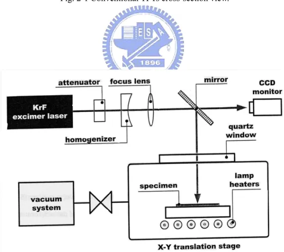
(21) Chapter 2 Fabrication and Characterization of Low-Temperature Poly-Si TFTs. 2.1 Typical Polysilicon TFT Fabrication Flow In our experiment, all TFT devices with new structures are compared with the conventional TFT device. The conventional TFT device is fabricated by 4 masks on the 4-inch-diameter silicon wafer, and the cross-section view of our conventional structure is shown in Fig. 2-1. The main fabrication procedure is listed as follows: 1. Thermal wet oxidation to grow starting SiO2 film 2. a-Si deposition by LPCVD system 3. Low-temperature crystallization of a-Si film to obtain poly-Si film 4. Mask #1: Poly-Si island definition (poly-Si dry etching by RIE system) 5. Deposition of gate dielectric layer by PECVD system 6. Poly-Si gate deposition by LPCVD system 7. Mask #2: Gate definition (poly-Si dry etching by RIE system) 8. Ion implantation for source/drain doping 9. Source/drain dopant activation 10. Deposition of final passivation layer by PECVD system 11. Mask #3: Contact holes definition 12. Thermal evaporation of aluminum layer 13. Mask #4: Metal pad definition 14. Aluminum sintering The detail parameters are illustrated in table 2-1.And the new sub-gate structure will be introduced in chapter 2 and 3, including cross-section view, fabrication procedure and operation principle..
(22) 2.2 Excimer Laser System The setup of excimer laser system used in our experiment is shown in Fig. 2-2. The key to the experiment is the KrF excimer laser and the wavelength of the one is 248 nm. In our experiment, the laser system was operated with frequency of 10 Hz and the pulse width of the laser pulse is approximately 30 ns. The samples are crystallized in a vacuum chamber at 320 mJ/cm2 energy density and 400℃ substrate heating with a pressure of < 10-3 torr.. 2.3 Methods of Device Parameter Extraction To evaluate the characteristics of poly-Si TFTs, we often depend on some parameters such as threshold voltage, subthreshold swing, field effect mobility and on/off current ratio. For quantitative analysis, explicit measurement methods and equations are necessary. Hence, we make brief definitions for these parameters and list some useful equations in this section. All the following measurement in my experiment is based on these definition and equations.. 2.3.1 Determination of Threshold Voltage The threshold voltage Vth is the most important parameter in MOSFET. But the way to decide the value is various. In this thesis, we use “linear extrapolation method” [2.1], and it is the most popular threshold voltage measurement technique at a low drain voltage. First, find the point of maximum slope on the ID-VGS curve by a maximum in the transconductance, g m =. ∂I DS , and then fit a straight line to the ∂VGS. ID-VGS curve at that point. Finally, extrapolate to ID=0, we get the value of VGSi . Put the values of VGSi and VDS into Vth = VGSi − VDS , the value of Vth appears 2. eventually..
(23) 2.3.2 Determination of Subthreshold Swing. Subthreshold swing S is that gate voltage necessary to change the drain current by one decade, and is given by S =. ln(10)nKT = 60n(T / 300) mV/decade [2.2]. It is a q. typical parameter to describe the control ability of gate toward channel. In this thesis, the subthreshold swing is defined as one-third of the gate voltage required decreasing the threshold current by three orders of magnitude. The threshold current is specified to be the drain current when the gate voltage is equal to threshold voltage.. 2.3.3 Determination of Field Effect Mobility. While the effective mobility is derived from the drain conductance, the field-effect mobility is determined from the transconductance [2.1]. The transconductance is defined by g m =. W ∂I DS = µ FE Cox ( )VDS . Besides, the definition ∂VGS L. of the drain current is that: I DS = µ FE Cox (. W 1 2 )[(VGS − Vth )VDS − VDS ] . Thus, we L 2. solve the equation (assume VDS approaches zero), and then the “field effect mobility” is given by: µ FE =. L g m (max) VDS →0 . CoxWVDS. 2.3.4 Determination of On/Off Current Ratio. In order to express not only large on-state current but also small off(leakage) current, we define a “on/off current ratio”, and it is one of the most important parameters of poly-Si TFTs. Theoretically, the leakage current is as smaller as better. But in poly-Si TFTs, the leakage mechanism is field emission via grain boundary traps by a high electric field near the drain. When the drain voltage increases, the leakage current will increase severely. Therefore, the voltage drops between drain and.
(24) source is as smaller as better when measures the on/off current ratio. In this thesis, the ratio is defined as following equation: I ON Maximum current of I DS − VGS plot at V DS = 0.1V = I OFF Minimum current of I DS − VGS plot at V DS = 0.1V. 2.4 Reliability Issue The low process temperature makes the reliability issues in LTPS TFTs different from those in the conventional MOSFETs. First, crystallized poly-Si is full of weak Si-Si bonds and dangling bond, and they will result in the variation of device electrical characteristics [2.3]. Then, the gate oxide grown at low temperature by PECVD system exhibits poor quality, such as low breakdown field, and high gate leakage current. Besides, the surface roughness of poly-Si resulting from laser crystallization will enhance local electrical field between the interface between poly-Si and gate oxide. Finally, “hot carrier effect” originates from high electric field near the drain region. It is also an important reliability issue in LTPS TFTs [2.4]. In this thesis, the stress condition is shown in table 2-1 [2.5]. The variations of the characteristics in different devices such as threshold voltage(Vth), subthreshold swing ( S.S ) and transconductance ( Gm ) will be as tabled. The degradation mechanism will be discussed, and we will compare different kinds of sub-gate structure and make a conclusion in practical production..
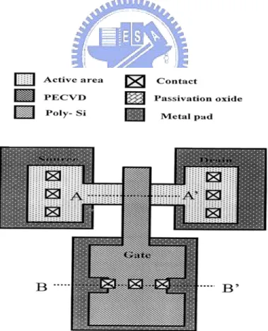
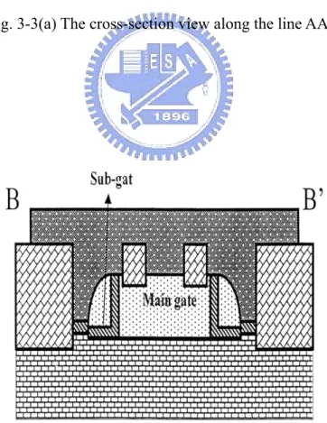
(25) Chapter 3 Poly-Si TFT with a Poly-Si Spacer Sub-Gate Structure. 3.1 Device Architectures Recently, LDD structure poly-Si TFTs are proposed to lower leakage current, but it also decrease the on-state current. Two years ago, our group proposed a new novel TFT structure with a self-aligned thicker sub-gate oxide near the drain/source region, which has a much lower off-state leakage current, and higher on/off current ratio than those of a conventional structure [3.1] At that time, the crystallization method for the deposited amorphous silicon is SPC(Solid Phase Crystallization)method at 600℃ for 24 hr. Nowadays, the most popular crystallization method in LTPS TFT technology is ELA(Excimer Laser Annealing) method. Therefore, we plan to combine the novel device structure and ELA method and suppose the on-state current can be further improved without sacrificing the off-state current. The schematic diagram of the proposed TFT structure is shown in Fig. 3-1. The top view of the proposed TFT structure is shown in Fig. 3-2, and the cross-section views along the line AA’ and BB’ are shown in Fig. 3-3(a) and (b). From the Fig. 3-3(b), we apply the voltage source on the sub-gates by opening new contact holes.. 3.2 Process Flow The TFTs were fabricated on 4-inch-diameter oxidized silicon wafer. A schematic graph of process flow is illustrated in Fig. 3-4. First, 100 nm-thick undoped a-Si thin films were deposited on 500 nm oxidized silicon ( 100 ) wafer by low-pressure chemical vapor deposition(LPCVD)system at 550℃ using silane (SiH4)gas. The deposition pressure was 100 mtorr and the silane flow rate was 40. sccm..
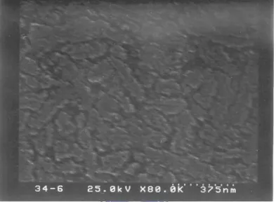
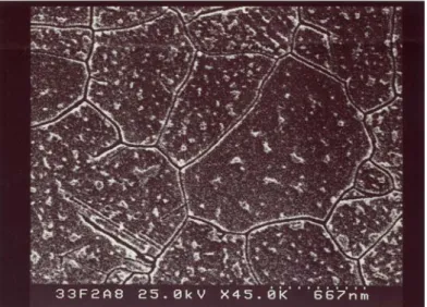
(26) Half the wafers were put into furnace and recrystallization was performed at 600℃ for 24 hr in N2 ambient using the SPC method. The other wafers were crystallized by KrF excimer laser annealing(ELA) in a vacuum ambient pumped down to 10-3 torr, in which the substrate temperature was controlled at 400℃. The excimer laser annealing was performed in the scanning mode at 320 mJ/cm2 energy density. After defining the device active regions, 50 nm-thick TEOS gate oxides were deposited by PECVD system. 300 nm-thick poly-Si films were then deposited by LPCVD system at 620℃ for the gate electrode. After defining the gate geometry, a 100 nm-thick PECVD TEOS oxide (Sub-gate oxide)and 400 nm-thick poly-Si layer were deposited alternately. The subsequent poly-Si films were etched by RIE system till the 100 nm-thick PECVD TEOS oxide, there were two sub-gate regions beside the gate electrode as shown in Fig. 3-1. A self-aligned 5×10¹⁵ ions/cm2 phosphorus implantation with a He-diluted PH3 gas at 50 KeV acceleration voltage was performed to form the regions of source, drain, sub-gate and gate electrodes. The dopant were activated at 600℃ in N2 ambient for 24 hr. Next, a 500 nm-thick TEOS oxide was deposited by PECVD system at 300℃ as a passivation layer. After contact holes were opened as shown in Fig. 3-2, a 500 nm-thick aluminum layer was deposited by thermal evaporation and the metal layer was patterned. Finally, the samples were sintered at 400℃ for 1 hr in N2 ambient. The process conditions of every step are listed in table 3-1(a)-(d).. 3.3 Analysis of Grain Size by Scanning Electron Microscope(SEM) 3.3.1 Sample Preparation. A-Si thin films with thickness of 100 nm were used as the starting material for SEM graph observation. The a-Si films were deposited on oxidized wafer with oxide.
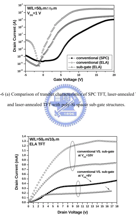
(27) thickness of 0.5µm using LPCVD system. After crystallization(whether SPC or ELA), the samples will be investigate the relation between the morphology of crystallized poly-Si thin films and electric characteristics through SEM observation. Before the analysis, the samples were processed by “Secco-etch”. “Secco-etch” preferably etches the grain boundaries in poly-Si and facilitate the SEM observation.. 3.3.2 SEM Graph Analysis and Discussion. Fig. 3-5(a) shows the SEM image of poly-Si film crystallized by SPC after Secco-etch. In this graph, we can observe that grains are generally elliptical in shape due to preferential growth in the <112> direction [3.2]. But, the low process temperature makes many defects exist in crystallized poly-Si. The average grain size by SPC in our experiment is about 100~200 nm. Fig. 3-5(b) and (c) show the SEM image of poly-Si film crystallized by ELA after Secco-etch. The graph indicates the grain size of ELA poly-Si film is indeed larger than the SPC one. In our experiment, the average grain size by ELA is about 1~1.5 µm. But there is a drawback in excimer laser system. In Fig. 3-5(d), the grain size are non-uniform distribution in poly-Si film [3.3]. It results in TFT devices which fabricated on these films have variant electrical characteristics. In order to give consideration to the consistency in our experiment, the device characteristic measurement is very important.. 3.4 The Characteristics of Laser-Annealed Poly-Si TFTs 3.4.1 Laser-Annealed Poly-Si TFTs with Poly-Si Spacer Sub-Gate Structures. Fig. 3-6(a) shows the comparison of transfer characteristics measured under a constant drain bias(VDS)of 1 V for SPC TFT, laser-annealed TFT and laser-annealed TFT with poly-Si spacer sub-gate structures. It was found that the characteristics.
(28) parameters of the TFTs crystallized by excimer laser annealing are better than the ones by SPC method, including threshold voltage(Vth),subthreshold swing(S),and on/off current ratio. It can be attributed to the larger grain size by excimer laser annealing, and there are no intra-grain defects in the grains. Thus, all the following devices in our experiment will be fabricated on excimer laser annealing poly-Si films. Table 3-3 summarizes the statistical data of the. electrical characteristics of. different ELA TFT devices. It shows the non-uniform electrical characteristics compared to those fabricated by SPC of a-Si. The reason for non-uniformity is mentioned in section 3.3.2. Compare the spacer sub-gate TFTs and conventional TFTs, the on-state current decreased from 2.96×10⁻⁴ A to 1.12×10⁻⁵ A(about one order), but the off-state current decreased substantially from 1.86×10⁻⁸ A to 1.46×10⁻¹⁰ A(at VGS=-5 V). The main reason for much lower off-state leakage current of the sub-gate TFT is the drain electric field is greatly reduced for the thicker gate oxide in the sub-gate regions and the self-aligned offset PECVD oxide. Although the on-state current degraded due to thicker gate oxide at the same time, the on/off current ratio still in the acceptable range. Fig. 3-6(b) shows the comparison of output characteristics(IDS-VDS)of sub-gate structure TFTs and conventional TFTs. It was observed that the kink effect is weak in sub-gate TFTs at VGS=6 V even the driving current is smaller [3.4]. It confirms the reduction of drain electric field.. 3.4.2 Laser-Annealed Poly-Si TFTs with Thicker Sub-Gate Nitride. In order to retrieve the degradation of driving current, we substitute nitride film for the gate dielectric of the sub-gate. Because the dielectric constant of nitride film is larger than oxide film, it can support higher driving current at the same thickness. In fig. 3-7, the sub-nitride TFT shows the better subthreshold swing and higher on-state current(about one order). On the contrary, the leakage current is also higher and.
(29) on/off current ratio is close to the sub-oxide TFT. The rise leakage current might be attributed to the traps of nitride/oxide interface or the poor interface between poly-Si gate and nitride [3.5].. 3.5 High Performance Sub-gate Structure TFTs with a Novel ONO Stack Gate Dielectric In order to improve the quality of gate dielectric, W. Z. Yang et al. have proposed a novel ONO stack gate dielectric. “ONO” means that N2O plasma oxide/ Si3N4/TEOS oxide tri-layer structure, and it is found that LTPS TFTs with a novel ONO stack gate dielectric structure have superior electrical properties, more remarkable reliability and lower interface trap density than traditional TEOS oxide ones. It was attributed to the high quality N2O plasma oxide forming smoother surface and strong Si≣N bonds at the oxide/poly-Si interface. Furthermore, the middle layer, Si3N4 film, which has higher dielectric constant than SiO2 results in promoting the on-state current of LTPS TFTs. Finally, the upper TEOS oxide layer was deposited due to improve the interface between gate dielectric and poly-Si gate. In section 3.4, we know that excimer laser annealed poly-Si TFTs with sub-gate structures has lower leakage current and higher on/off current ratio than conventional structure ones. But the drawback of sub-gate structure is that on-state driving current also slightly decrease at the same time. For the sake of high on-state current and low leakage current, we fabricate excimer laser annealed sub-gate structure TFTs with ONO stack gate dielectric. It shows that they have more excellent electrical properties and good reliability. The ONO stacked gate dielectric grown parameters are listed in table 3-2. Fig. 3-8(a) shows the comparison of transfer characteristics measured under a constant drain bias(VDS)of 1 V for sub-gate TFTs with TEOS oxide and ONO stack.
(30) gate dielectric. It was found that the characteristics parameters of the TFT with ONO are promoted obviously, including the higher on-state current(from 3.06×10⁻⁵ to 1.95×10⁻⁴, about one order), the better subthreshold swing and threshold voltage. And the on/off current ratio is 8.44×10⁷. Thus, the combination of sub-gate structure and ONO gate dielectric can get excellent device characteristics. Fig 3-8(b) shows the comparison of output characteristics(IDS-VDS)of sub-gate structure TFTs with TEOS oxide and ONO stack gate dielectric. The driving current of sub-gate TFT with ONO at VDS=18 V is 3.08×10⁻⁴(VGS=6V)and 9.71×10⁻⁴(VGS=10V). The reducing current by sub-gate structure could be compensated for ONO gate dielectric and the kink effect is also eased. Fig. 3-9 shows the comparison of all the devices in this chapter and the detailed data were listed in table 3-4.. 3.6 Reliability Issues The stability of device characteristics under long-time operation is important especially as data driver in AMLCDs and pixel element in AMOLEDs. Many reasons will lead to device degradation such as gate oxide quality, poly-Si crystallization quality, self-heating, surface roughness of poly-Si and hot carrier effects. For this reason, reliability issues in LTPS TFTs are also very important research topics. Fig. 3-10 (a) and (b) show the degradation of the maximum transconductance and the threshold voltage variations under static hot-carrier stress which is defined as the TFT being kept at a high electric field in the drain junction. Notably, the dc stress conditions are VGS =10V and VDS =20V. The △Vth is defined as Vth,s –Vth, i where Vth, i. denotes the initial Vth and Vth, s represents the Vth for etch stress time. Moreover, the. degradation of the Gm max is defined as △Gm max /Gm max, i ,where △Gm max = △Gm max, s. - △Gm max, i, Gm max, i denotes the initial Gm max and Gm max, s represents the Gm max for.
(31) each stress time. The △Vth and △Gm max /Gm max, i are measured at 1.0 V for etch stress time. In fig. 3-10 (a), the sub-gate structure TFT shows better reliability in transconductance than conventional one. It could be attributed to the reduction of drain electric field and weaken the hot carrier effect. At the region of the stress time between 1 sec and 100 sec, the slope of the threshold voltage shift of sub-gate structure was larger than that of the conventional structure. This is because that there were many weak bonds at the interface of the sub-gate oxide and active region, and the weak bonds were broken during the stress. Then, the traps were generated additionally and made threshold voltage increased rapidly [3.6]. After long time stress about 10000 sec, the stress generated traps of both structures saturated with time and the slope variations of them were almost the same.. 3.7 Summary The sub-gate structure with a self-aligned thicker sub-gate oxide near the drain/source regions has leakage current lower on order than those of the conventional one. For the sake of larger driving current, we introduce the silicon nitride to the thicker layer. Although the on-state driving current increased, the on/off current ratio is nearly unchanged due to higher leakage current. Finally, the sub-gate structure TFT with ONO stack gate dielectric shows the excellent properties. It shows the leakage current 100 times lower than those of the conventional ones and also shows on/off current ratio of 8.44×10⁷ at VGS=-5 V and VDS=1 V. The degradation of the maximum transconductance and the threshold voltage variations under static hot-carrier stress of sub-gate structure is also less than conventional one..
(32) Chapter 4 Laser-Annealed Poly-Si TFT with a Floating Sub-Gate Structure. 4.1 Device Architectures In order to reduce leakage current in LTPS TFTs, several structures have been proposed, for example, offset gated structures. But, it needs an additional photo-masking step and increases extra series resistance. The misalignment problem would also occur. We proposed a poly-Si TFT with a sub-gate coupling structure and will reduce the off state current without degrading the on current [4.1]. Besides, an additional interfacial amorphous silicon layer will be deposited. The following variation in device electrical characteristics and reliability is worthy to observe and discuss. The schematic diagram of the sub-gate structure TFT is shown in Fig. 4-1. The top view of the proposed TFT structure is shown in Fig. 4-2(a), and the cross-section views along the line AA’ and BB’ are shown in Fig. 4-2(b) and (c).. 4.2 Process flow The process flow of fabricating sub-gate coupling structure TFT is the same as the conventional non-offset poly-Si TFT. And the process conditions are also the same as the conventional poly-Si TFT. The detailed fabrication process flow is listed as follows. 1. (100) orientation Si wafer. 2. Initial cleaning. 3. Thermal wet oxidation at 1050。C to grow 500 nm thermal SiO2 in furnace. 4. 1000 Å a-Si was deposited by LPCVD at 550。C in SiH4 gas. 5. KrF excimer laser crystallization was carried out in 10-4 Torr at 320 mJ/cm2.
(33) energy density and 400。C substrate heating. 6. Mask #1:Define active regions (poly-Si dry etching by Poly-RIE system). 7. RCA cleaning. 8. 50 nm gate dielectric deposition by PECVD at 300。℃. 9. 300 nm poly-Si was deposited by LPCVD at 620。C in SiH4 gas. 10. Mask #2:Define gate regions (poly-Si dry etch by Poly-RIE system). 11. Ion implantation: P31 , 50KeV, 5x10¹⁵ ions/cm2. 12. Dopant activation in N2 ambient at 600。C for 24hrs in furnace. 13. 500 nm TEOS oxide was deposited by PECVD as passivation layer. 14. Mask #3:Open contact holes 15. 500 nm Al thermal evaporation. 16. Mask #4:Al pattern defined. 17. Etching Al and removing photoresist. 18. Al sintering at 400。C in N2 ambient for 1 hr.. 4.3 Electrical Properties and Characteristics Fig. 4-3 shows the comparison of transfer characteristics measured under a constant drain bias(VDS)of 0.1V and 5V for laser-annealed TFT and laser-annealed TFT with a floating sub-gate structure. It was found that the laser-annealed TFT with a floating sub-gate structure has the smaller leakage current(about two order), and on/off current ratio is close to the ratio of the conventional TFTs(2.12×10⁷ and 4.28× 10⁷). Because of the lower leakage current, we suppose it is helpful to device reliability. The sub-gate is floating and its potential is controlled by the main gate potential VGS, drain potential VDS, undoped channel potential VUC, and doped channel potential.
(34) VDC. The VSG can be expressed as: VSG =. 1 (C1 ⋅ VMG + C 2 ⋅ VDS + C 3 ⋅ VUC + C 4 ⋅ VDC ) , CT. where CT=C1+C2+C3+C4. C1,C2,C3,and C4 are the capacitances between the sub-gate and the bottom layer, drain region, undoped channel, and doped channel, respectively. The parameter R=AMS/ASC where AMS is overlapping area between the metal pad and the sub-gate and ASC is overlapping area between the sub-gate and the channel. In off state, the VGS<0 and the VDS>0.Thus, the sub-gate potential determined by above equation is smaller than the main gate potential. The drain electric field can be reduced as compared to the conventional TFTs, so the sub-gate TFT can act as the offset poly-Si TFT in the off state if the area ratio R is properly adjusted. In the on state, both VGS and VDS>0. The sub-gate potential is almost equivalent to the main gate potential at high VGS and VDS, so that the sub-gate TFT behaves as the conventional TFT in the on state. Fig. 4-4 (a)-(c) shows the effect of area ratio R on IDS-VGS characteristics at VDS=0.1, 1 and 5V. As R increases up to 10, the sub-gate TFT behaves as the conventional TFT. On the other hand, as R decreases down to 1, the sub-gate TFT acts as an offset TFT. Fig. 4-5 (a) and (b) show the effect of area ratio R on IDS-VDS characteristics at VGS=6 and 10V. It was found that the kink effect is weaker when R decreases, but the driving current is also degraded. Thus, modulating the R value is an important issue. Fig. 4-6 shows the off state leakage current measured at VGS=-5V and the on state current measured at VGS=20V for various area ratio R. We need the on state current larger and the off state current smaller. Thus the optimum condition of the floating sub-gate TFT can be achieved at R=5. All the detailed data about sub-gate TFT with various R were listed in table 4-1..
(35) 4.4 Improving the Characteristics of Low-Temperature Poly-Si TFTs by an Additional Amorphous Silicon Interfacial Layer Comparing to SPC method, the surface of the excmier laser crystallized poly-Si films is rather rough due to the explosive protrusion of grain boundaries during the grain growth, which results in the increase of the roughness at the poly-Si/gate oxide interface. It is also reported that the field-effect mobility of TFT devices is affected by the roughness of the gate insulator [4.2]. Considerable efforts have been paid to improve the surface roughness of poly-Si because the electrical characteristics of TFT’s are seriously affected by the interface roughness of the gate insulator [4.3]. In this section, we introduce a thin amorphous silicon nano layer on the poly-Si channel layer, and combine the floating sub-gate structure to investigate the effect of the surface roughness on the device performance, including studied the transfer characteristics. The transfer characteristics(IDS-VDS) of laser-annealed sub-gate TFT(R=5) with/without α-Si layer are shown in Figure 4-7(a) and (b). Both on state current (measured at VGS= 20 V) and off-state leakage current (measured at VGS= -5 V) are reduced with a-Si layer thickness increasing. The reason for lower leakage current of the laser-annealed TFT with ultra-thin a-Si layer is due to reduction of the drain electric field [4.4]. However, it was found that the turn-on current is also degraded when the a-Si layer thickness increased. We supposed the reduction of the turn-on current due to higher grain boundary trap density of a-Si layer became dominate. It is obviously that the optimum condition is ELA with 5 nm-thick a-Si layer. At VDS = 5 V, the on/off current ratios of the ELA TFT and the ELA TFT with 5-nm a-Si layer are 7.59 x 10⁴ and 2.96 x 10⁵, respectively. The detailed data and parameters are shown in table 4-2. Fig. 4-8(a) and (b) shows the transfer characteristics measured under a constant.
(36) drain bias(VDS)of 1 V and 5 V for the floating sub-gate TFT with 5-nm a-Si layer. The leakage current of the floating sub-gate TFT with 5-nm a-Si layer is still getting lower when the area ratio R decreased. But, the turn-on current at low drain voltage (VD=1V)has the peak point to conduct. We suppose the dual channel layer(poly-Si. and ultra-thin a-Si layer)result in a multi-conducting path and choose the lowest resistivity path. Fig. 4-9 shows the comparison of output characteristics(IDS-VDS)of sub-gate structure TFT(R=5) with/without 5-nm a-Si layer. Less kink effect is observed in sub-gate TFT with ultra-thin a-Si layer and we can further confirm that the drain electric field is effectively reduced as a-Si layer thickness increasing. Because the kink current in TFT device is basically due to the avalanche or impact ionization in the device and it is strongly influenced by grain boundary traps. The grain boundary traps can prevent the channel carriers from gaining higher energy, and therefore the impact ionization probability can be reduced as the grain boundary trap density is increased. Fig. 4-10(a) and (b) show the comparison of transfer characteristics(IDS-VGS) measured under a constant drain bias(VDS)of 1 V and 5 V for the conventional TFT and the floating sub-gate TFT with/without 5-nm a-Si layer. It was found that the lowest leakage current is gotten by combining the floating sub-gate structure and the ultra-thin a-Si layer. And the on/off current ratio is close to the one of conventional TFT. Fig. 4-11(a) shows the off state leakage current measured at VGS=-5V and the on state current measured at VGS=20V of the floating sub-gate TFT with 5-nm a-Si layer for various area ratio R. It is identical to fig. 4-6 that without a ultra-thin a-Si layer. And fig. 4-11(b) shows the off state leakage current measured at VGS=-5V and the on state current measured at VGS=20V of the floating sub-gate TFT(R=5)for various a-Si layer thickness. It is shown that both on and off current degraded when a-Si thickness increased. All the detailed data and parameters are listed in table 4-3..
(37) 4.5 Reliability Issues As usual, reliability issues are still the important topics that we are concerned. Fig. 4-12 (a) and (b) show the degradation of the maximum transconductance and the threshold voltage variations under static hot-carrier stress which is defined as the TFT being kept at a high electric field in the drain junction. Notably, the dc stress conditions are VGS =10V and VDS =20V. In fig. 4-12 (a), the sub-gate structure TFT shows better reliability in transconductance than conventional one. It has been extensively discussed that Gm max degradation during hot-carrier stress conditions is mainly due to interface state generation. Due to the sub-gate structure decreasing the drain electric field, the hot carrier effect is quite reduced. In fig. 4-12 (b), both structure show almost the same power-time dependence. The mechanism of Vth variations includes hot carrier injection into the gate oxide and deep grain-boundary trap generation [4.5]. Due to the sub-gate structure decreasing the drain electric field, both of them are reduced. Thus, sub-gate structure shows better device reliability.. 4.6 Summary The floating sub-gate structure behaves as an offset gated structure by modulating overlapping area ratio R, and its fabrication processes is fully the same as the conventional TFT. The optimum condition is R=5 in this thesis. It shows the leakage current is 3.51×10⁻¹⁰ A and is 100 times lower than those of the conventional ones at VGS=-5 V and VDS=1 V. It also shows on/off current ratio of 2.12×10⁷ at VGS=-5 V and VDS=1 V. In order to improve the surface roughness of poly-Si film, we cap an ultra-thin a-Si layer on the laser-annealed poly-Si film. And it show better electrical characteristics. The sub-gate structure(R=5)TFT with a 5 nm-thick a-Si capping layer shows the low leakage current of 2.4×10⁻⁹ A and on/off current ratio of 5.85×10⁶ at VGS=-5 V and VDS=1 V. The degradation of the maximum.
(38) transconductance and the threshold voltage variations under static hot-carrier stress of sub-gate structure is also less than conventional one..
(39) Chapter 5 Conclusions and Future Works 5.1 Conclusions The sub-gate structure with a self-aligned thicker sub-gate oxide near the drain/source regions has leakage current lower on order than those of the conventional one. For the sake of larger driving current, we introduce the silicon nitride to the thicker layer. Although the on-state driving current increased, the on/off current ratio is nearly unchanged due to higher leakage current. Finally, the sub-gate structure TFT with ONO stack gate dielectric shows the excellent properties. It shows the leakage current 100 times lower than those of the conventional ones and also shows on/off current ratio of 8.44×10⁷ at VGS=-5 V and VDS=1 V. The degradation of the maximum transconductance and the threshold voltage variations under static hot-carrier stress of sub-gate structure is also less than conventional one. The floating sub-gate structure behaves as an offset gated structure by modulating overlapping area ratio R, and its fabrication processes is fully the same as the conventional TFT. The optimum condition is R=5 in this thesis. It shows the leakage current is 3.51×10⁻¹⁰ A and is 100 times lower than those of the conventional ones at VGS=-5 V and VDS=1 V. It also shows on/off current ratio of 2.12×10⁷ at VGS=-5 V and VDS=1 V. In order to improve the surface roughness of poly-Si film, we cap an ultra-thin a-Si layer on the laser-annealed poly-Si film. And it show better electrical characteristics. The sub-gate structure(R=5)TFT with a 5 nm-thick a-Si capping layer shows the low leakage current of 2.4×10⁻⁹ A and on/off current ratio of 5.85×10⁶ at VGS=-5 V and VDS=1 V. And It also shows better device reliability than conventional structure TFT. Therefore, the combination techniques of novel ONO stack gate dielectric, ELA.
(40) crystallization method, additional ultra-thin a-Si layer and sub-gate structures for fabricating poly-Si TFTs exhibit significantly superior electrical characteristics and reliability to the conventional poly-Si TFTs. Hence, they are promising for the application of integrated circuits on AMLCD panels.. 5.2 Future Works There are some interesting topics that are valuable for the future further research about the LTPS TFTs. If appropriate plasma passivation is performed for optimized thinner silicon films, the carrier mobility and gate voltage swing would be further improved. Although excimer laser has been shown to be the most promising candidate for the crystallization method of LTPS TFTs, the instability and short pulse duration of excimer laser makes the formation of uniform and large grained poly-Si thin films hard. The continuous-wave(CW)laser may be another alternative for crystallizing a-Si thin films due to the advantages of good stability of laser fluence and long melting duration during laser irradiation..
(41) References Chapter 1 [1.1] P. K. Weimer, “The TFT- A New Thin-Film Transistors”, Proc. IEEE 50, pp.1462, 1962. [1.2] T. P. Brody et al., “A 6’’×6’’ 20 Lines-per-Inch Liquid Crystal Display Panel”, in. SID Tech. Dig., pp. 179, 1973. [1.3] H. C. Tuan, “Amorphous Silicon Thin Film and Its Applications to Large-Area Elements”, Mater. Rec. Soc. Ump. Proc., vol.33, pp.247, 1984. [1.4] I-W. Wu, “Cell Design Considerations for High-Aperture-Ratio Direct-View and Projection Poly-Silicon TFT-LCDs”, in SID Tech. Dig., pp. 19-22, 1995. [1.5] M. G. Clark, “Current Status and Future Prospects of Poly-Si Devices”, IEEE. Proc.-Circuits Devices Syst., vol.141, no.1, February 1994. [1.6] A. Nakamura et al., “A High-Reliability, Low-Operation-Voltage Monolithic Active-Matrix LCD by Using Advanced Solid-Phase Growth Technique”, in. IEDM Tech. Dig., pp.847, 1990. [1.7] Eric Campo et al., “Influence of Rapid Thermal and Low Temperature Processing on the Electrical Properties of Polysilicon Thin Film Transistors”,. IEEE Trans. On Semi. Manufacturing, vol.8, no.3, August 1995. [1.8] Zhiguo Meng et al., “High Performance Low Temperature Metal-Induced Unilaterally Crystallized Polycrystalline Silicon Thin Film Transistors for System-on-Panel Applications”, IEEE Trans. Electron Devices, vol.47, no.2, February 2000. [1.9] Seok-Woon Lee et al., “Fabrication of High-Mobility P-Channel Poly-Si Thin Film Transistors by Self-Aligned Metal-Induced Lateral Crystallization”, IEEE. Electron Device Lett., vol.17, no.8, August 1996. [1.10] Won Kyu Kwak et al., “A High Performance Thin-Film Transistors Using a.
(42) Low Temperature Poly-Si by Silicide Mediated Crystallization”, IEEE Electron. Device Lett., vol.21, no.3, March 2000. [1.11] N. Kubo et al., “Characterization of Polycrystalline-Si Thin-Film Transistors Fabricated by Excimer Laser Annealing Method”, IEEE Electron Device Lett., vol.40, pp.1876-1879, October 1994. [1.12] G. K. Giust and T. W. Sigmon, “Low-Temperature Polysilicon Thin-Film Transistors Fabricated from Laser-Processed Sputtered-Silicon Films”, IEEE. Electron Device Lett., vol.19, pp.343-344, September 1998. [1.13] G. K. Giust and T. W. Sigmon, “High-Performance Laser-Processed Polysilicon Thin-Film Transistors”, IEEE Electron Device Lett., vol.20, no.2, pp.77-79, February 1999. [1.14] W. G. Hawkins, “Polycrystalline-Silicon Device Technology for Large-Area Electronics”, IEEE Trans. Electron Devices, vol.33, pp.477-481, 1986. [1.15] J. W. Lee et al., “Oxidation of Silicon Using Electron Cyclotron Resonance Nitrous Oxide Plasma and Its Application to Polycrystalline Silicon Thin Film Transistors”, J. Electrochem. Soc., vol.133, pp.3238, 1997. [1.16] C. C. Chen et al., “Plasma-Induced Charging Damage in Ultrathin (3nm) Nitrided Oxide”, IEEE Electron Device Lett., vol.21, pp.15-17, January 2000. [1.17] K. R. Olasupo and M. K. Hatalis, “Leakage Current Mechanism in Sub-Micron Polysilicon Thin-Film Transistors”, IEEE Trans. Electron Devices, vol.43, pp.1218-1223, 1996. [1.18] M. Lack et al., “Analysis of Leakage Current in Poly-Silicon Thin Film Transistors”, in IEDM Tech. Dig., pp.385-388, 1993. [1.19] K. Tanaka et al., “Characteristics of Offset-Structure Polycrystalline-Silicon Thin-Film Transistors”, IEEE Electron Device Lett., vol.9, no.1, pp.23-25, January 1988..
(43) [1.20] B. H. Min et al., “A Novel Offset Gated Polysilicon Thin Film Transistor Without an Additional Offset Mask”, IEEE Electron Device Lett., vol.16, no.5, pp.161-163, May 1995. [1.21] C. M. Park et al., “Self-Aligned Offset Gated Poly-Si TFT’s with a Floating Sub-Gate”, IEEE Electron Device Lett., vol.18, no.1, pp.16-18, January 1997. [1.22] B. H. Min and Jerzy Kanicki, “Electrical Characteristics of New LDD Poly-Si TFT Structure Tolerant to Process Misalignment”, IEEE Electron Device Lett., vol.20, pp.335-337, 1999. [1.23] K. M. Chang et al., “A Novel High-Performance Poly-Silicon Thin Film Transistors with a Self-Aligned Thicker Sub-Gate Oxide near the Drain/Source Regions”, IEEE Electron Device Lett., vol.22, no.10, pp.472-474, October 2001. [1.24] K. M. Chang et al., “Characterization of the Novel Polysilicon Thin Film Transistors with a Subgate Coupling Structure”, IEEE Trans. Electron Devices, vol.49, no.4, pp.564-567, April 2002. [1.25] K. M. Chang et al., “Electrical Characteristics of Low Temperature Polysilicon TFT with a Novel TEOS/Oxynitride Stack Gate Dielectric”, IEEE Electron. Device Lett., vol.24, no.8, pp.512-514, August 2003.. Chapter 2 [2.1] Dieter K. Schroder, Semiconductor Material and Device Characterization,. Wiley-INTERSCIENCE, 1998. [2.2] S. M. Sze, Physics of Semiconductor Devices, 2nd edition, John Wiley & Sons, 1981. [2.3] I-Wei Wu et al., “Mechanism of Device Degradation in n- and p-Channel Polysilicon TFT’s by Electrical Stressing”, IEEE Electron Device Lett., vol.11, no.4, pp.167-170, April 1990..
(44) [2.4] N. D. Young et al., “Hot Carrier Degradation in Low Temperature Processed Polycrystalline Silicon Thin Film Transistors”, Semicond. Sci. Technol., vol.7, pp.1183-1188, May 1992. [2.5] C. W. Lin et al., “Effects of Plasma Treatments, Substrate Types, and Crystallization methods on Performance and Reliability of Low Temperature Polysilicon TFTs”, in IEDM Tech. Dig., pp.305-308, 1999.. Chapter 3 [3.1] K. M. Chang et al., “A Novel High-Performance Poly-Silicon Thin Film Transistors with a Self-Aligned Thicker Sub-Gate Oxide near the Drain/Source Regions”, IEEE Electron Device Lett., vol.22, No.10, pp.472-474, October 2001. [3.2] A. Nakamura et al., “Recrystallization Mechanism for Solid Phase Growth of Poly-Si Films on Quartz Substrate”, Jpn. J. Appl. Phys. Part2, vol.27, pp. L2408-L2410, 1988. [3.3] James S. Im and H. J. Kim, “On the Super Lateral Growth Phenomenon Observed in Excimer Laser-Induced Crystallization of Thin Si Films”, Appl.. Phys. Lett., vol.64, pp,2303-2305, 1994. [3.4] Anish Kumar et al., “Kink-Free Polycrystalline Silicon Double-Gate Elevated-Channel Thin-Film Transistors”, IEEE Trans. Electron Devices, vol.45, no.12, pp.2514-2520, December 1998. [3.5] Nobuki Ibaraki et al., “The Effect of Interface States on Amorphous-Silicon Transistors”, IEEE Trans. Electron Devices, vol.36, no.12, pp.2971-2972, December 1989. [3.6] F. V. Farmakis et al., “Anomalous Turn-On Voltage Degradation During Hot-Carrier Stress in Polycrystalline Silicon Thin-Film Transistors”, IEEE. Electron Device Lett., vol.22, No.2, pp.74-76, February 2001..
(45) Chapter 4 [4.1] K. M. Chang et al., “Characterization of the Novel Polysilicon Thin Film Transistors with a Subgate Coupling Structure”, IEEE Trans. Electron Devices, vol.49, no.4, pp.564-567, April 2002. [4.2] Akito Hara et al., “Mobility Enhancement Limit of Excimer-Laser-Crystallized Polycrystalline Silicon Thin Film Transistors”, J. Appl. Phys., vol.91, pp. 708-714, 2002. [4.3] Kyung Wook Kim et al., “A Polycrystalline Silicon Thin-Film Transistor with a Thin Amorphous Buffer”, IEEE Electron Device Lett., vol.20, No.11 pp.560-562, November 1999. [4.4] Anish Kumar et al., “Kink-Free Polycrystalline Silicon Double-Gate Elevated-Channel Thin-Film Transistors”, IEEE Trans. Electron Devices, vol.45, no.12, pp.2514-2520, December 1998. [4.5] F. V. Farmakis et al., “Anomalous Turn-On Voltage Degradation During Hot-Carrier Stress in Polycrystalline Silicon Thin-Film Transistors”, IEEE. Electron Device Lett., vol.22, No.2, pp.74-76, February 2001..
(46) The process parameters in conventional TFTs 1. Thermal oxide. 5000 Å. 2. Amorphous silicon. 1000 Å. 3. Crystallization. Excimer laser annealing. 4. Mask #1. 5. Gate oxide. TEOS oxide 500 Å. 6. Poly-Si Gate. 3000 Å. 7. Mask #2. 8. Ion Implantation. 5×1015 cm-2 , 50 KeV. 9. Dopant activation. 600 ℃, 24 hr. 10. Passivation layer. 5000 Å. 11 12. Mask #3 Aluminum evaporation. 13 14. 5000 Å. Mask #4 Aluminum sintering. 400 ℃, 1 hr. Table 2-1 Process parameters in conventional TFTs. Hot carrier stress VDS=20 V VGS=10 V ( 10000 sec ) Table 2-2 Stress condition.
(47) Gas source. Flow rate. Pressure. Temperature. (sccm). (mtorr). (℃). 40. 100. 550. SiH4. Table 3-1(a) Process conditions of amorphous silicon deposited by LPCVD system.. Gas source. Flow rate. Pressure. Temperature. (sccm). (mtorr). (℃). 40. 120. 620. SiH4. Table 3-1(b) Process conditions of polysilicon deposited by LPCVD system.. Gas source. Flow rate. RF power. Pressure. (sccm). (W). (mtorr). 100. 20. SF6. 20. O2. 4. Table 3-1(c) Process conditions of polysilicon dry etching by RIE system.. Gas source. Flow rate. RF power. Pressure. Temperature. (sccm). (W). (pa). (℃). 300. 90. 350. TEOS. 450. O2. 7. Table 3-1(d) Process conditions of TEOS oxide(gate oxide)deposited by PECVD system..
(48) Gas source. N2O. Flow rate. RF power. Pressure. Temperature. (sccm). (W). (mtorr). (℃). 200. 200. 100. 300. (a) 1st layer:N2O plasma oxide.. Gas source. Flow rate. RF power. Pressure. Temperature. (sccm). (W). (mtorr). (℃). 50. 500. 300. N2. 500. SiH4. 20. NH3. 80 (b) 2nd layer:nitride.. Gas source. Flow rate. RF power. Pressure. Temperature. (sccm). (W). (mtorr). (℃). 100. 200. 300. TEOS. 10. O2. 600. (c) 3rd layer:TEOS oxide. Table 3-2 The ONO stacked gate dielectric grown parameters..
(49) μFE(cm2/V*s). ELA TFTs. SPC TFTs. Mean ofμFE. 118.75. 15.33. % of μFE. 29.31. 15.85. Mean of Vth. 5.32. 12.36. % of Vth. 10.7. 2.7. Table 3-3 Statistical data of the electrical characteristics of LTPS TFT fabricated by different crystallization manners. Five TFTs were measured in each case.. Conventio ONO Sub-nitride Sub-oxide nal TFTs -4 -4 1.24×10⁻⁴ 3.06×10⁻⁵ On current at VGS=20 V 2.96×10 1.95×10 (A) -12 -12 -12 5.16×10⁻¹² Minimum current (A) 5.08×10 2.31×10 5.45×10 On/Off current ratio. 5.83×10⁷ 8.44×10⁷. 2.28×10⁷. Leakage current at VGS=-5V (A). 1.86×10⁻⁸ 2.25×10⁻¹⁰ 3.38×10 -10. Table 3-4 Summary table of device parameters of all kinds of spacer sub-gate poly-Si TFTs.. 5.93×10⁶ 4.74×10⁻¹¹.
(50) Conventio nal TFTs. R=10. R=5. Threshold voltage (V). 5.41. 4.86. 3.5. Subthreshold swing (mV/dec). 609. 573. 554. Field-effect mobility (cm2/V-sec). 144.86. 42.88. 127.48. -5 -5 1.49×10⁻⁵ On current at VGS=20 4.26×10 2.71×10 V (A) -13 -12 -13 Minimum current (A) 9.94×10 1.41×10 7.03×10. On/Off current ratio. 4.28×10⁷ 1.92×10⁷. 2.12×10⁷. Leakage current at VGS=-5V (A). 7.48×10⁻⁸ 4.25×10⁻¹⁰ 3.51×10 -10. Table 4-1 Summary table of device parameters of ELA sub-gate TFTs(different R).. Conventio nal TFTs. 50 Å. 100 Å. 200 Å. Threshold voltage (V). 5.21. 5.13. 6.07. 7.33. Subthreshold swing (mV/dec). 735. 937. 1680. ------. Field-effect mobility (cm2/V-sec). 127.48. 73.5. ------. ------. On current at VGS=20 V (A). 1.04×10⁻⁴ 3.90×10⁻⁵. 3.64×10⁻⁵ 1.91×10⁻⁷. Minimum current (A). 3.05×10⁻¹² 6.75×10⁻¹². 4.33×10⁻¹² 2.49×10⁻¹¹. On/Off current ratio. 3.41×10⁷ 5.78×10⁶. Leakage current at VGS=-5V (A). 4.13×10⁻⁹ 2.40×10⁻⁹. 8.41×10⁶. 1.31×10³. 1.67×10⁻¹⁰ 2.53×10⁻¹¹. Table 4-2 Summary table of ELA sub-gate TFTs(R5)with different a-Si thickness..
(51) Conventio nal TFTs. R=10. R=5. R=3. R=1. Threshold voltage (V). 5.33. 5.24. 5.21. 5.13. 6.02. Field-effect mobility (cm2/V-sec). 83.9. 77.4. 73.5. 66.3. 54.3. 1.16×10⁻⁵. 3.15×10⁻⁶. On current at VGS=20 V 1.14×10⁻⁴ 1.05×10⁻⁴ 3.95×10⁻⁵ (A) Minimum current(A) 3.51×10⁻¹² 1.35×10⁻¹¹ 6.75×10⁻¹² On/Off current ratio Leakage current at VGS=-5V (A). 6 3.25×10⁷ 7.78×10. 5.85×10⁶. 1.34×10⁻⁸ 2.37×10⁻¹⁰ 2.40×10⁻⁹. 9.73×10⁻¹² 3.44×10⁻¹² 1.19×10⁶. 9.16×10⁵. 7.22×10⁻¹¹ 8.17×10⁻¹¹. Table 4-3 Summary table of ELA + 50Å a-Si sub-gate(different R)TFTs..
(52) Fig. 1-1 Offset TFT structure.. Fig.1-2 LDD TFT structure..
(53) Fig. 2-1 Conventional TFTs cross-section view.. Fig. 2-2 The schematic diagram of the sub-gate structure TFT..
(54) Fig. 3-1 The schematic diagram of the poly-Si spacer sub-gate structure.. Fig. 3-2 The top view of the poly-Si spacer sub-gate structure..
(55) Fig. 3-3(a) The cross-section view along the line AA’.. Fig. 3-3(b) The cross-section view along the line BB’..
數據

+7
相關文件
• 後段工程是從由矽晶圓切割成一個一個的晶片 入手,進行裝片、固定、接合連接、注模成 形、引出接腳、按印檢查等工序,完成作為元
在1980年代,非晶矽是唯一商業化的薄膜型太 陽能電池材料。非晶矽的優點在於對於可見光
Now, nearly all of the current flows through wire S since it has a much lower resistance than the light bulb. The light bulb does not glow because the current flowing through it
In section29-8,we saw that if we put a closed conducting loop in a B and then send current through the loop, forces due to the magnetic field create a torque to turn the loopÆ
雙極性接面電晶體(bipolar junction transistor, BJT) 場效電晶體(field effect transistor, FET).
The development of IPv6 was to a large extent motivated by the concern that we are running out of 4-byte IPv4 address space.. And indeed we are: projections in- dicate that the
To reduce the leakage current related higher power consumption in highly integrated circuit and overcome the physical thickness limitation of silicon dioxide, the conventional SiO
To reduce the leakage current related higher power consumption in highly integrated circuit and overcome the physical thickness limitation of silicon dioxide, the conventional SiO 2
