國 立 交 通 大 學
電機工程學系
電信工程研究所
博 士 論 文
具立體通道之矽奈米級金氧半場效應電晶體
本質參數擾動之研究
Intrinsic Parameter Fluctuation in Nanoscale
MOSFET with Vertical Silicon Channels
研 究 生:黃至鴻
指導教授:李義明 教授
立體通道之矽奈米級金氧半場效應電晶體本質參
數擾動之研究
Intrinsic Parameter Fluctuation in Nanoscale
MOSFET with Vertical Silicon Channels
研究生:黃至鴻
Student:
Chih-Hong
Hwang
指導教授:李義明 博士 Advisor:
Dr.
Yiming
Li
國立交通大學
電機工程學系 電信工程研究所
博士論文
A Dissertation
Submitted to Institute of Communication Engineering
Department of Electrical Engineering
College of Electrical and Computer Engineering
National Chiao Tung University
in Partial Fulfillment of the Requirements
for the Degree of Doctor of Philosophy
in
Electrical Engineering
Hsinchu, Taiwan
c
° Copyright by Chih-Hong Hwang 2009
All Rights Reserved
摘 要
延續摩爾定律而獲得高性能矽晶片以及高密度元件之觀點,新材料、新製程與 新結構的開發是半導體製造上繼續微縮元件的尺寸最有效的策略方案;其中,16 奈 米之後電晶體結構的改變儼然已成為非常前瞻與重要的趨勢,因此研究隨機摻雜問 題與製程變異在多重閘極場效電晶體特性之影響已為重要且急迫之課題之一。因此 本論文發展了三維度元件電路模擬技術使用等效原子層級離散摻雜暨量子傳輸方程 的大尺度統計運算方法,並成功地分析 16 奈米立體矽場效應電晶體特性之擾動由 單閘極、雙閘極、三閘極至全閘極電晶體。此研究方法之準確度已成功地以次 20 奈 米矽場效應電晶體特性之實驗驗證。相較於單閘極電晶體,臨界電壓擾動在雙閘極、 三閘極至全閘極分別被壓抑 2.2、3.3 與 4 倍,壓抑的原理及物理特性均有探討。此 外,近來金屬閘極與高介電係數材料的使用已成為奈米電晶體元件開發之重要課 題,但金屬閘極的使用將因金屬材料本身結晶顆粒的大小與方向帶來另外的擾動來 源,因此本論文發展蒙地卡羅方法廣泛的分析閘極功函數擾動、離散摻雜擾動與製 程變異在多重閘極場效電晶體特性暨其電路之影響,發現閘極功函數擾動對於金屬 閘極電晶體尤其是 p-type 元件之重大影響,此論文結果對於電晶體擾動壓抑之推估 以及下世代電晶體特性擾動分析極有助益。 ivAbstract
Gate-length scaling is still the most effective way to continue Moore’s Law for transistor density increase and chip performance enhancement. Accompanied with complementary metal-oxide-semiconductor (CMOS) technology advanced to 32-nm node in production, further scaling down to sub-20 nm and even beyond has been widely noticed encountering much more challenges at short channel control than previous generations. The worsened short channel control of nanoscale transistor not only increases standby power dissipation, but also enlarges electrical characteristic fluctuations, such as the deviation of threshold voltage, drive current, mismatch, and so on. The fluctuation budget has to be controlled even tighter due to doubly increased transistor number along with technology node mov-ing ahead. Moreover, the fluctuation is intrinsically increased with the scalmov-ing of transistor feature size, even not considering worsened short channel control. This thesis describes the intrinsic parameter fluctuations in vertical-channel devices from planar transistor to
double gate, tri-gate, omega fin-type field effect transistors (FinFETs) and nanowire Fin-FETs through experimental validated three-dimension device simulation and characteriza-tion. The implication of device variability in nanoscale transistor circuits are advanced. The extensive study assesses the fluctuations on device and circuit reliability, which can in turn be used to optimize nanoscale MOSFET and circuits. Full realization of the bene-fit of nanoscale transistor therefore requires development and optimization of new device materials, structures, and technologies to keep transistor performance and reliability.
誌
謝
六年前的夏天,回憶的片段像口試時撥放的投影片,一頁頁略過我的腦海。當初那個羞澀 中帶有點稚氣的年輕人又映入我的眼簾,背景的圖案從工程四館、電資大樓、校門口的土地公 廟到交大的校園的每一處不停的變換,中間閃過了日本、希臘、法國、美國等充滿異國風情的 背景,最後回到了一張多人的大合照。曾幾何時,那笨拙稚氣的年輕人已穿上了西裝露出微笑, 眼角泛著淚光,曾幾何時,那本來瘦弱的臂膀已變得強壯而結實,這一切的一切都要感謝照片 中所有人的陪伴、支持與鼓勵。 年輕人右手邊的是他的指導教授 李義明老師,他是帶給照片那位年輕人影響最多的人。 多年的悉心指導、專業知識的傳授、研究方法的推敲、用字遣辭之斟酌以及為學處世待人接物 謹慎積極的態度,讓那位年輕人在治學方法及處世態度上受益良多,尤其是在論文發表時常退 居幕後,讓學生站在國際的舞台上發光發熱,更是年輕一輩學子日後之表率。值得一提的是李 老師右手邊的 周復芳老師與 李育民老師,兩位老師在修業期間提供的教誨與最大的自由度 與支持讓學生得以進行感興趣的研究。在幾位老師身旁的是論文口試期間提供寶貴意見與殷切 指正讓論文更臻完備的成大電機工程學系 王水進老師、清華大學電機工程學系 白田里一郎老 師、清華大學工程與系統科學系 張廖貴術老師與交通大學電子工程學系 陳明哲老師。師恩細 長,深切銘心,學生在此謹獻上最誠摯的感謝與敬意。 年輕人的左手邊是他平行科學計算實驗室的好伙伴:正凱、紹銘、素雲、惠文、益廷、大 慶、宣銘、典燁、毓翔、英傑、國輔、銘鴻、紀寰、忠誠及俊諺,正凱學長神人般留傳的程式 庫、紹銘學長的熱情教學與呵呵微笑、同窗好友的互相砥礪,如繞樑之音盤旋在腦海。年輕人 身後還有他一群共患難的朋友:金玲、逸宏、闡哥、酷桑、阿琅、小宇、培育、哲宇、獻哲, 謝謝你們,尤其是金玲,與妳在一起的六個年頭,有苦有笑點滴在心頭,謝謝妳一路的陪伴。 感謝這群陪伴我渡過許多困難的好友,學業的路上沒有你們,再美好的風景都覺得索然無味。 畫面轉回到身後的家人,感謝之詞溢於言表,謝謝你們在背後默默的支持與忍耐,你們是我最 大的力量來源,讓我在疲憊的時候給我最大的鼓勵與支持,請讓我用行動表達心中的感謝。 投影片到了最後的一頁,感謝行政院國家科學委員(計畫編號:NSC-96-2221-E-009- 210、 NSC- 95-2221-E-009-336、NSC-95-2752-E-009-003-PAE、 NSC-97-2221-E-009-154- MY2)、卓 越延續計畫(計畫編號:NSC-95-2752-E-009-003-PAE、NSC-96-2752-E-009-003-PAE)、五年五 百億計畫、群創光電股份有限公司、台灣積體電路製造股份有限公司產學研究計畫之經費補 助。感謝台積電楊副處長富量博士(現國家奈米元件實驗室主任)與黃經理俊仁博士提供研究 上的協助。能順利完成博士學業,全靠父母、家人及諸位朋友、同學的支持與忍耐,對此由衷 感謝,謹在此將本論文獻給關心我的人。 黃至鴻 謹誌 中華民國九十八年十月 于交通大學 viiContents
Abstract . . . v
Acknowledgments . . . vii
List of Tables . . . xiii
List of Figures . . . xv
1 Introduction 1 1.1 Toward Nanoscale Transistor Era . . . 1
1.2 Vertical Channel Transistor Architecture . . . 5
1.2.1 FinFET Process Steps . . . 7
1.2.2 Process Simulation Using TCAD . . . 8
1.3 Current Research Status and Motivation . . . 10
1.4 Outline . . . 15 2 Device Model and Numerical Methods 17
x CONTENTS
2.1 The Quantum-Mechanical Corrected Transport Equations . . . 17
2.1.1 The Density-Gradient Equations . . . 17
2.1.2 The Mobility Model . . . 21
2.2 The Numerical Simulation Methods . . . 22
2.2.1 The Gummel Decoupling Method . . . 22
2.2.2 The Adaptive Finite Volume Method . . . 25
2.2.3 The Monotone Iterative Method . . . 28
2.3 A 25-nm FinFET Simulation and Calibration . . . 30
2.4 Summary . . . 45
3 Simulation of Intrinsic Parameter Fluctuation 47 3.1 Process Variation Effect . . . 48
3.2 Random-Dopant-Induced Characteristics Fluctuation . . . 50
3.2.1 Discrete Dopant Generation Method . . . 52
3.2.2 Kinetic Monte Carlo Simulation . . . 56
3.3 Workfunction fluctuation . . . 59
3.4 Calibration and Verification . . . 67
3.5 Summary . . . 75 4 Random-Dopant-Induced Characteristics Fluctuation in Vertical-Channel
CONTENTS xi
4.1 Bulk Fin-Type Field Effect Transistors . . . 78
4.1.1 Roll-Off Characteristics . . . 79
4.1.2 Comparison with Planar MOSFETs with High-κ Dielectrics . . . . 93
4.2 Silicon-on-Insulator Transistors . . . 105
4.3 Summary . . . 126
5 Intrinsic Parameter Fluctuation in Fin-Typed Field Effect Transistors 128 5.1 DC Characteristic Fluctuation . . . 129
5.2 AC Characteristic Fluctuation . . . 134
5.3 Summary . . . 143
6 Implication of Device Variability in Circuits 145 6.1 The Coupled Device-Circuit Simulation Technique . . . 146
6.2 Digital Circuits . . . 151
6.3 Analog/High-Frequency Circuits . . . 168
6.4 Summary . . . 179
7 Conclusions and Future Work 181 7.1 Conclusion of This Study . . . 181
7.2 Suggestions on the Suppression Approaches . . . 182
xii CONTENTS
7.2.2 Inverse Lateral Asymmetry Doping Profile . . . 188 7.3 Suggestions on the Future Work . . . 191 References . . . 194 Appendix A
List of Tables
2.1 Material parameters setting for silicon, poly-silicon, SiO2 and Si3N4. The
epsilon is the ratio of the permittivities of material and vacuum. . . 40 3.1 The trend of Vthfor technology scaling. The nominal Lg cases in table are
nominal gate lengths for each technology node respectively. . . 73 3.2 Summary of experimental and simulation results of discrete dopant
fluctu-ated 20-nm-gate planar CMOS transistors. . . 73 4.1 The the threshold voltage fluctuation induced by S/D dopants only, channel
dopants only, and fully discrete schemes and the simulation time for one transistor. . . 79 4.2 Threshold voltage of the studied devices with nominal continuous channel
doping . . . 82 4.3 Summary of the threshold voltage fluctuation of the explored planar
MOS-FETs and bulk FinMOS-FETs. . . 105 xiii
xiv LIST OF TABLES
6.1 Transition time variation for the 16-nm-gate planar inverter circuits. (* normalized by the nominal value) . . . 158 6.2 Summarized high-frequency characteristic fluctuations of the nano-MOSFETs
circuit. . . 175 7.1 Effectiveness of vertical doping profile engineering and lateral asymmetry
List of Figures
1.1 The major sources of intrinsic parameter fluctuations: the gate length devi-ation, line edge roughness, and random dopant fluctuation [15]. . . 2 1.2 Experimental saturation threshold voltage of NMOSFETs with Lgdown to
20 nm for the (a) width = 200 nm and (b) width = 20 nm at VD = 1.0 V. . . 3
1.3 Experimental Ion-Iof f characteristics of NMOSFETs with Lg down to 20
nm for the (a) width = 200 nm and (b) width = 20 nm at VD = 1.0 V. The
Ion was normalized against the on-current of nominal Lg case, i.e. the 20
nm Lgcase. . . 3
1.4 The evolution of transistor architecture from planar MOSFETs to ultra-thin-body silicon-on-insulator, double-gate, omega gate, and nanowire Fin-FETs. . . 6
xvi LIST OF FIGURES
1.5 The process simulation result for FinFETs. ((a)-(a”))The device structure after Si fin patterning, STI. The doping concentration in this step is back-ground doping with 1.0×1015 cm−3 boron concentration.((b)-(b”))After
Well/Vth implantation and annealing, the dopants are activated after
ther-mal annealing. The fabrication process then goes to gate formulation, pocket and LDD implantation. The gate oxide is formulated after the gate oxide growth ((c)-(c”)). ((d)-(d”))After spacer formation and source/drain implantation, the final device structure is shown. . . 9 1.6 The gate length deviation, line edge roughness, and random dopant
fluctu-ation induced Vthfluctuation versus equivalent oxide thickness (EOT). . . . 11
1.7 The threshold voltage fluctuation versus technology node. . . 13 2.1 The plot of FV method. (a) One-Irregular mesh, and (b) the difference
between finite element mesh and finite volume mesh . . . 26 2.2 The mesh used for the solution process. . . 27 2.3 (a) An illustration of the simulated fin-type field effect transistors. The
top of the fin is formed to a round shape naturally and the fin bottom is not actually rectangular for the lithography and silicon etching processes. (b) The ID-VG curves for the FinFETs. The red and black lines are the
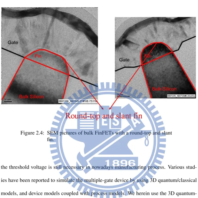
LIST OF FIGURES xvii 2.4 SEM pictures of bulk FinFETs with a round-top and slant fin. . . 32 2.5 (a) The device dimension and parameter setting of the simulated fin-type
field effect transistors, in which the device workfunction is 4.28 eV. (b) The characteristics of the ID-VG curves for the FinFETs. The red and black
lines are the simulated and measured data, respectively. The simulation shows a good agreement with measurement data, which represents the ac-curacy of the calibrated 3D device simulation. . . 33 2.6 Three-dimensional schematic plots for the (a) bulk FinFETs and (b) SOI
FinFETs. Θ is the fin angle and the inset shows a 2D cutting-plane extract-ing from the center of channel. . . 35 2.7 (a) A plot of the 3D doping profile of the round-top-gate bulk FinFET. The
left plot is the contour of doping profile and the right one is the correspond-ing mesh. (b) The left plot is the on-state potential of the round-top bulk FinFET and the right one is the off-state potential. . . 36 2.8 Plots of the 2D cutting plane of the simulated on-state (VD = 1.0 V and VG
= 1.0 V) (a) potential and (b) electron density at the center of channel of the 30 nm-height bulk FinFET. The fin angles are the 90o, 80o , and 70o,
xviii LIST OF FIGURES
2.9 Plots of the 2D cutting plane of the on-state (a) potential and (b) electron density at the center of channel of the 40 nm-height bulk FinFET. The fin angles are the 90o, 80o, and 70o, respectively. . . 38
2.10 Plots of the 2D cutting plane of the on-state ((a) potential and (b) electron density at the center of channel of the 50 nm-height bulk FinFET. The fin angles are the 90o, 80o, and 70o, respectively. . . 39
2.11 Plots of 1D cutting lines of the potential and electron density at the center of channel. The device is with the fin height of (a) 30 nm, and (b) 50 nm, where the solid line is the result of 90o, the dotted line is for the 80o, and
the dashed line is for the 70o. The circled windows indicate the regimes
where nearly constant potential and electron density are occurred in device channel. . . 42 2.12 (a) The ID-VG curves for the device for different fin angles and heights.
The solid lines are the result of 90o, the dotted lines are for the 80o, and the
dashed lines are for the 70o. (b) Results of SS (the left plot) and DIBL (the
right one) versus the fin angle, where the solid lines are the result of 30 nm, the dotted lines are for the 40 nm, and the dashed lines are for the 50 nm. . 44
LIST OF FIGURES xix 3.1 (a) An illustrates for the result of generated profile. The
process-variation-effect induce gate length variation, σLg,P V E, are obtained. The inset shows
the equation for the estimation of σVth,P V E. (b)A look-up table of the
threshold voltage versus gate length. Using the Vth roll-off relation, the
σVth,P V E can be obtained. . . 48
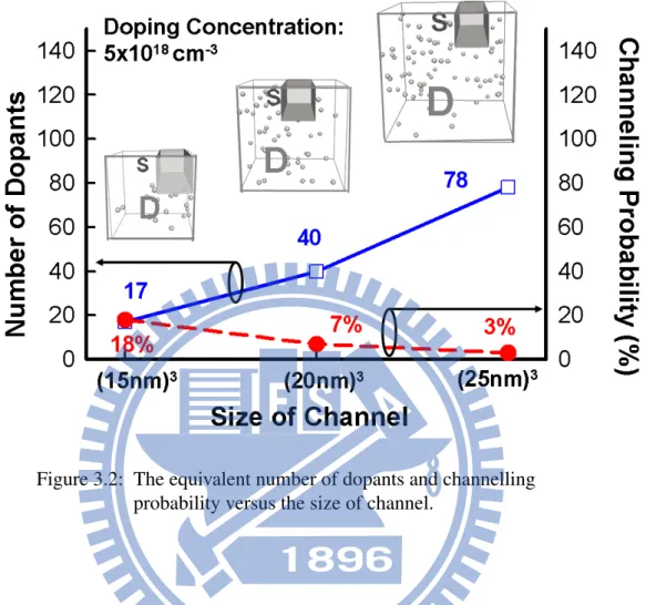
3.2 The equivalent number of dopants and channelling probability versus the size of channel. . . 51 3.3 (a) Discrete dopants randomly distributed in (100 nm)3 cube with an
av-erage concentration of 5×1018 cm−3. 5000 dopants are in the (100 nm)3
cube, but dopants vary from 24 to 56 (the average number is 40 and the standard deviation is 6.3) within its sub-cubes of (20 nm)3, (the (b), (c),
and (e)). These sub-cubes are then equivalently mapped into channel re-gion for RDF simulation, as shown in the (d). . . 53 3.4 (a) Discrete dopants randomly distributed in (150 nm)3 cube with average
concentration of 1.48×1018 cm−3. 5000 dopants are within the cube, but
dopants may vary from 26 to 55 (average number is 40) within each of the sub-cubes of (30 nm)3, [(b) and (d)]. The sub are then used for RDF
simulation (c). The statistically generated discrete-dopant distributions for (e)22- and (f)16-nm-gate length. . . 55
xx LIST OF FIGURES
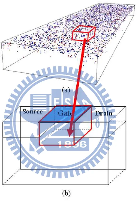
3.5 Integration of kinetic Monte Carlo (KMC) atomistic process simulation with atomistic device simulation. (a) The KMC simulation generated dopant distribution. The Kinetic Monte Carlo simulation is therefore used to mimic the dopant distribution inside silicon channel. (b) The generated dopant distribution is then mapped into device channel for simulation. . . 57
3.6 (a) The distribution of KMC simulated profile. The solid line is the dopant distribution, which can be replaced by SIMS profile. The dash line is the fitted distribution, which is similar to the original dopant distribution. (b) The generated 5000 dopants, whose distribution along the Si/SiO2interface
is similar to the original profile, the solid line in (a). . . 58
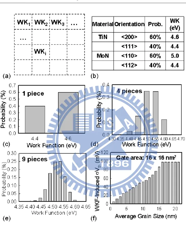
3.7 (a) The SEM pictures and illustration of TiN surface, which containing numbers of grain with various grain orientation. (b) An illustration of crys-tal structure of copper with <200>, and <111> orientation. Each grain orientation has its own strength of dipoles and therefore different work-function. Therefore, the combination of device workfunction will become a probabilistic distribution rather than a deterministic value. . . 60
LIST OF FIGURES xxi 3.8 The gate area is partitioned into several pieces according to the average
grain size. The workfunction of each partitioned area (W Ki) is a random
value, whose probability follows (b). The obtained probability distributions of TiN workfunction for devices with (c) 1, (d) 4, and (e) 9, grains on the gate area. (f) Dependence of TiN metal-gate induced σVth,W KF versus the
average grain size. The gate area is 16 × 16 nm2 . . . 62
3.9 WKF induced Vth fluctuation versus average grain size with and without
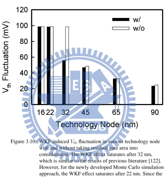
taking residual gate area into consideration. The inset illustrates the resid-ual gate area during the discritization of gate area. The flat area in the solid line may mislead the impact of WKF. . . 64 3.10 WKF induced Vthfluctuation in various technology node with and without
taking residual gate area into consideration. The WKF effect saturates after 32 nm, which is similar to the results of previous literature [122]. However, for the newly developed Monte Carlo simulation approach, the WKF effect saturates after 22 nm. Since the average grain size is 22 nm, having the same Vthfluctuation after 22 nm is reasonable. . . 65
3.11 Potential profiles for (a) classical (b) and quantum potential with different mesh size. . . 68
xxii LIST OF FIGURES
3.12 Meshing and dopant distribution for (a) long channel and (b) nanoscale transistors. The fine mesh in nanoscale transistor creates problems of sin-gularities in the Coulomb potential and un-physically trap majority carriers. 69 3.13 (a) Extracted non-strain mobility versus doping concentration at 0.3 and 1
MV/cm vertical field, and (b) scaling of average channel dopant numbers versus channel size. . . 71 3.14 (a) Experimentally extracted σVth,RDF, and discrete-dopant simulation (*,
Lg= W = 20 nm, EOT = 1.2 nm) for various devices with nominal Lgfrom
55 nm down to 20 nm. The width is fixed and the length is varying to give the range of values of (WL)−0.5. The sample size for each data point of V
th
is around 100 points. (b) The extracted σVth,P V E for c and d conditions.
The value was normalized against the σVth,P V E of nominal Lg case in d
condition. . . 72 4.1 (a) The dopant distributions for the fully discrete scheme in 16-nm-gate
transistor. Both source/drain and channel dopants are placed randomly in device. (b) The associated potential distribution, in which the effective device gate length was disturbed. . . 80
LIST OF FIGURES xxiii 4.2 For cases with 1.48×1018 cm−3 average channel doping concentration,
the maximum differences in threshold voltage induced by discrete-dopant-position effect for 30-, 22-, and 16-nm-gate-lengths, which are normalized by the corresponding nominal threshold voltage. . . 83 4.3 Fluctuations of threshold voltage for the 30-, 22- , and 16-nm-gate bulk
FinFETs. The threshold voltages of the studied devices are normalized by the corresponding nominal threshold voltage. . . 84 4.4 On-off state current characteristics of the 30-, 22- , and 16-nm-gate bulk
FinFET devices. . . 85 4.5 Plot of threshold voltage roll-off for the 30-, 22- , and 16-nm-gate bulk
FinFETs, where the bars indicate the fluctuation of threshold voltage. . . . 86 4.6 Fluctuations of threshold voltage roll-off (i.e., versus the Lg) of bulk
Fin-FETs and planar MOSFin-FETs. . . 87 4.7 Threshold voltage fluctuation as a function of device dimension. (a) Plots
of dependence factor on γ for various device dimensions. (b) Fluctuation of threshold voltage for the 60-nm-gate device was assumed to be 1 mV. . . 88
xxiv LIST OF FIGURES
4.8 (a) The characteristics of ID-VG, where the solid line indicates the
contin-uous (i.e., the nominal) case. The fluctuations of (b) on-state current, (c) off-state current and (c) threshold voltage as a function of the number of dopants. . . 89
4.9 The on-state potential distributions of the 16-nm-gate bulk FinFETs with six discrete dopants inside the channel (average concentration: 1.48×10¹⁸
cm−3), and the nominal case. The potential distributions are 2 nm below
the top and lateral gates. The potential distributions for the device with (a) minimal threshold voltage (b) nominal threshold voltage and (c) maximal threshold voltage. . . 90
4.10 (a) The characteristics of Ion-Iof f of the 125 discrete-dopant 16-nm-gate
bulk FinFETs. Three cases are selected to evaluate similar Ionbut different
Iof f (plots of (b) and (c)) and similar Iof f but different Ion(plots of (c) and
(d). Plots of (b)-(d) and (b’)-(d’) show the corresponding top and lateral views of the on-state current density, which are extracted at the 1 nm below the gate oxide, respectively. Plots of (b”)-(d”) show the off-state potential contours. . . 92
LIST OF FIGURES xxv 4.11 The gate capacitance as a function of the EOT, where the solid line shows
the planar MOSFETs with various EOT and the square symbol indicates the bulk FinFET device with 1.2 nm EOT. . . 94 4.12 The process-variation-induced threshold voltage fluctuation for the studied
devices. . . 95 4.13 The threshold voltage roll-off of the studied devices, where the variation
follows the projection of ITRS 2005 roadmap. These results are used to estimate the Vth fluctuation resulting from the gate-length deviation and
the line-edge roughness. . . 96 4.14 The random-dopant-induced threshold voltage fluctuation for the studied
devices. . . 97 4.15 Top-gate potential contours of the planar MOSFETs with various EOT ((b)
EOT = 1.2 nm, (c) EOT = 0.8 nm, (d) EOT = 0.4 nm, (e) EOT = 0.2 nm) and (f) bulk FinFETs with 1.2 nm EOT. The distributions of potential barriers are induced by the corresponding dopants location (i.e., A, B and C). The corresponding distribution of discrete dopants is shown in (a) and all the plots are extracted 1 nm below the gate oxide. . . 98
xxvi LIST OF FIGURES
4.16 Lateral-gate off-state potential contours for the studied planar MOSFET and bulk FinFET devices, where (b) and (c) show the nominal (continu-ously doped) and discrete dopant fluctuated cases of bulk FinFETs. The nominal and discrete dopant fluctuated cases of planar MOSFETs with dif-ferent EOTs are shown in (d)-(h). . . 99
4.17 Cross-sectional views of on-state current density distribution in channel of device, where (b), (c), and (d) show the planar MOSFET device and (e), (f), and (g) show the bulk FinFET device. The corresponding distribution of discrete dopants is shown in (a) and all the cross-section plots are extracted 1 nm below the channel surface. . . 102
4.18 Ion-Iof f current characteristics of the studied 16-nm-gate planar MOSFET
and bulk FinFET devices. . . 103
4.19 Total threshold voltage fluctuation for the studied devices. . . 104
4.20 The (a) single-gate; (b) double-gate; (c) triple-gate; and (d) quadruple surrounding-gate for the dopant position/number-sensitive device simulation.106
LIST OF FIGURES xxvii 4.21 Comparison of the on-state potential contours ((b) and (b’)), the current
density distributions ((c) and (c’)), the electric field ((d) and (d’)), the elec-tron velocity ((e) and (e’)), and the elecelec-tron temperature ((f) and (f’)) of the (a) the nominal case and (a’) discretely doped cases. The potential spikes (marked as A, B, and C) in (b’) are induced by corresponding dopants in (a’)). All cross-sectional plots of the on-state current density distributions and off-state potential contours are extracted at 1 nm below the top-gate oxide. . . 107 4.22 The ID-VGcharacteristics of the 500 discrete-dopant-fluctuated 16-nm-gate
single- and multiple-gate SOI devices, where the solid lines indicate the nominal case and the dash lines indicate the discretely doped cases. . . 109 4.23 The on-off state current characteristics of the 500 discrete-dopant-fluctuated
16-nm-gate single- and multiple-gate SOI devices. (a) Comparison be-tween the single- and double-gate devices. (b) Comparison among the double-, triple-, and quadruple surrounding-gate devices. . . 110 4.24 (a) Comparison of Vth fluctuation of the 16-nm-gate single- and
multiple-gate SOI MOSFETs. (b) Plots of the standard deviation (S.D.) and the maximum difference of Vthwith respect to different gate number. . . 111
xxviii LIST OF FIGURES
4.25 Plots of the on-state potential and 3D electric field distribution of the 16-nm-gate SOI MOSFET with the (b) single- (c) double-, (d) triple- and (e) quadruple surrounding-gate structure. The cross-sectional plots of the on-state potential distributions are extracted along the center of the device’s channel, as shown in (a). . . 114 4.26 Plots of the on-state current density distributions ((a)-(d)) and the off-state
potential contours ((a’)-(d’)) of the 16-nm-gate SOI MOSFETs ((a) and (a’) are for the single-gate; double-gate: (b) and (b’); triple-gate: (c) and (c’); quadruple surrounding-gate: (d) and (d’)). The potential spikes in (a’)-(d’) are induced by corresponding dopants in channel (spikes A, B, and C shown in (a)). The height of potential spikes is decreased as gate number is increased. All cross-sectional plots of the on-state current density dis-tributions and off-state potential contours are extracted at 1 nm below the top-gate oxide. . . 115 4.27 Plots of the lateral-side ((a)-(d)) and bottom-gate ((a’)-(d’)) on-state current
density distributions of the 16-nm-gate devices ((a) single-gate; (b) double-gate; (c) triple-double-gate; (d) quadruple surrounding-gate). All cross-sectional figures are extracted at 1 nm below the lateral-side and bottom-gate oxides. 116
LIST OF FIGURES xxix 4.28 The 16-nm-gate silicon nanowire transistor with structures of (a)
surrounding-gate (i.e., 100% coverage), (b) the omega-surrounding-gate with 80% coverage-ratio, and (c) the omega-gate with 70% coverage-ratio. . . 118 4.29 Comparison of the on-state potential ((a) and (b)), the current density
dis-tributions ((e) and (f)) of the (c) the nominal case and (d) discretely doped cases. The potential fluctuations are induced by corresponding dopants in (d)). . . 119 4.30 Comparison of potential (plots of (a’), (b’), and (c’)) and current
den-sity distribution (plots of (a”), (b”), and (c”)) in nanowire transistors with surrounding-gate (100% gate-coverage-ratio) and omega-gate (80% and 70% gate-coverage-ratio) structures. . . 121 4.31 Comparison of the threshold voltage fluctuation of the 16-nm-gate
sili-con nanowire FET with surrounding-gate, omega-gate with 80%, and 70% gate-coverage-ratio. . . 122 4.32 Comparison of the on-off state current fluctuation of the 16-nm-gate
sili-con nanowire FET with surrounding-gate, omega-gate with 80%, and 70% gate-coverage-ratio. . . 123 4.33 Effect of discrete-dopant-position in silicon nanowire FET, where the
xxx LIST OF FIGURES
4.34 Effect of discrete-dopant-position in silicon nanowire FET, where the de-vices are with similar Ionbut different Iof f . . . 125
5.1 (a) An illustration of FinFET structure. 1516 dopants are randomly gener-ated in a large cube of 80×80×160 nm3, in which the equivalent doping
concentration is 1.48×1018 cm−3. The large cube is then partitioned into
125 sub-cubes of 16×16×32 nm3. The number of dopants in sub-cube
may vary from two to 22, and the average number is 13 ((b)-(d)). These 125 sub-cubes are equivalently mapped into the device channel of device for the 3D device simulation with discrete dopants. (e) The Vth roll-off is
used for PVE estimation. The PVE includes the gate length deviation and the line edge roughness, whose magnitude follow the projections of the ITRS roadmap [1]. (f) The σVth,W KF is estimated by a statistically sound
Monte-Carlo approach. ((g)-(i)) Similarly, 758 dopants are generated in a large cube of 80×80×80 nm3 and into 125 sub-cubes of 16×16×16 nm3
for planar MOSFETs discrete dopant simulation. . . 130 5.2 The ID-VGfluctuations for (a) NMOSFETs and (b) PMOSFETs, where the
solid line shows the nominal case with expected device dimensions, work-function, and 1.48×1018 cm−3 continuous channel doping. The dashed
LIST OF FIGURES xxxi 5.3 The summarized Vth fluctuation for (a) NMOSFETs and (b) PMOSFETs,
where the filled-in bars are the results of planar MOSFETs and the open bard are the results of FinFETs. . . 133 5.4 The Cg-VGcharacteristics for the explored devices with (a) PVE, (b) WKF,
and (c) RDF. (d) The Cgfluctuation for 16-nm-gate MOSFETs with WKF,
PVE, and RDF. The applied voltage for the bars are VG = 0, 0.5, and 1 V,
respectively. . . 137 5.5 The (a) Cg-VG curves and (b) the slope of the Cg-VG curves for cases
with and without taking random-dopant-position effect into consideration, where the solid line shows the nominal case and the dashed lines are random-dopant-fluctuated devices. The solid and dot lines in (a) are the cases with and without random-dopant-position effect, respectively. The dash line in (b) indicates the cases without random-dopant-position effect, and the sym-bols are the cases with random-dopant-position effect. The (c) normalized gate capacitance fluctuation and (d) maximum gate capacitance fluctuation are calculated. (e) The C fluctuation with different drain bias. . . 138 5.6 The Cg fluctuation for planar MOSFETs and SOI FinFETs with WKF,
PVE, and RDF. The filled-in bars are the results of planar MOSFETs and the open bars are the results of SOI FinFETs. . . 139
xxxii LIST OF FIGURES
5.7 The (a)WKF, (b)PVE, and (c) RDF induced FT characteristics fluctuation
of planar MOSFETs. (d)The summarized FT fluctuations. . . 141
5.8 The (a)WKF, (b)PVE, and (c) RDF induced FT characteristics fluctuation
of FinFETs. (d)The summarized FT fluctuations. . . 142
6.1 Time domain coupled device circuit simulation flow [64-67,115-118]. The characteristics of the devices of the circuit are first estimated by solving the device transport equations. The obtained result is then used as initial guesses in the coupled device-circuit simulation. The nodal equations of the test circuit are formulated and then directly coupled to the device trans-port equations, which are solved simultaneously to obtain the devices and circuit characteristics. . . 147 6.2 The (a) inverter circuit and (b) common source amplifier circuits as
exam-ples for digital and analog/high-frequency characteristics fluctuation explo-ration. . . 148 6.3 (a) The voltage transfer curves for the studied 16-nm-gate planar MOSFET
circuit. (b) The noise margins, NMLand NMH, as a function of the dopant
LIST OF FIGURES xxxiii 6.4 (a) The input and output signals for the discrete-dopant-fluctuated
16-nm-gate planar inverter circuit. The magnified plots show (b) the fall and (c) the rise transitions, where the rise time, fall time, high-to-low delay time, and low-to-high delay time are defined. . . 154 6.5 The fluctuations of (a) fall and (b) rise signal transition points as a function
of dopant number in n-type and p-type MOSFETs for the discrete dopant fluctuated inverter circuits. . . 155 6.6 The fluctuations of (a) high-to-low and (b) low-to-high delay time as a
function of dopant number in n-type and p-type MOSFETs for the discrete dopant fluctuated inverter circuits. . . 156 6.7 The fluctuations of (a) the fall and (b) rise time as a function of the
thresh-old voltage in the n-type and p-type MOSFETs for the discrete-dopant-fluctuated CMOS inverters. . . 159 6.8 Comparison of the variations of (a) tHL and (b) tLH with respect to WKF,
PVE, and RDF for the planar MOSFETs and FinFETs. . . 162 6.9 The nominal power for the bulk planar MOSFET and SOI FinFET inverter
circuits. . . 163 6.10 The (a) dynamic power, (b) short-circuit power, (c) static power, and (d)
xxxiv LIST OF FIGURES
6.11 The common-source circuit is used as a tested circuit to explore the fluctu-ation of high-frequency characteristics. The input signal is a sinusoid input wave with 0.5 V offset. The frequency is sweep from 1×10⁸ Hz to 1×10¹³
Hz. . . 167 6.12 DC characteristic fluctuations of (a) gm,max, and (b) ro of the 125 discrete
dopant fluctuated 16-nm-gate planar MOSFET. The definitions are shown in the insets. . . 168 6.13 The (a) voltage-transfer-curve, (b) the output voltage, (c) the voltage gain,
(d) and the fluctuation of voltage gain for the studied discrete-dopant-fluctuated 16-nm-gate common-source circuits. The solid line shows the capacitance of the nominal case (continuously doped channel with 1.48×1018 cm−3
doping concentration) and the dashed lines are the random-dopant-fluctuated devices. . . 169 6.14 The output signal fluctuation of the discrete-dopant-fluctuated circuits at
108 Hz. The solid line is the nominal case and the dashed lines are
transis-tors with discrete dopants. . . 170 6.15 The (a) frequency response, (b) high-frequency circuit gain, (c) 3dB
band-width, (d) and unity-gain bandwidth fluctuations of the studied discrete-dopant-fluctuated 16-nm-gate common-source circuits. . . 172
LIST OF FIGURES xxxv 6.16 Output power, circuit gain, and power-added-efficiency of the explored
de-vices as a function of input power. . . 175 6.17 The circuit gain characteristics of the planar MOSFETs with (a)PVE, (b)WKF,
and (c)RDF fluctuations, respectively. (d) The summarized circuit fluctua-tions. . . 176 6.18 (a) The frequency response of the planar MOSFET and FinFET
common-source amplifiers, in which (b) 3dB bandwidth, (c) gain, and (d) unity-gain bandwidth are extracted. . . 178 7.1 There will be 758 dopants are within a large rectangular solid, in which the
equivalent doping concentration is 1.48×1018cm−3). The dopant
distribu-tion in the direcdistribu-tion of channel depth follows the normal distribudistribu-tion (a). Similarly, dopants within the (16 nm)3cubes may vary from zero to 14 (the
average number is six) (b). The vertical dopant distribution of the vertical doping profile engineering and the original doping profile are shown in (c) and (d), respectively. . . 183 7.2 DC characteristic fluctuations of the 250 discrete dopant fluctuated
16-nm-gate planar MOSFET from the original and the improved doping profile. The studied fluctuations of (a) threshold voltage, (b) on-state current, (c)
xxxvi LIST OF FIGURES
7.3 (a) Comparison of frequency response fluctuations of the discrete dopant fluctuated 16-nm-gate cases generated from the improved (dashed line) and original (solid line) doping distributions. Comparison of (a) Gain, (b) 3dB bandwidth, (c) and unity-gain bandwidth fluctuations of the 125 discrete dopant fluctuated 16-nm-gate planar MOSFET circuit with the improved (squares) and original (”×”) doping profiles. . . 185 7.4 (a) Illustration of conventional and proposed lateral asymmetry doping
pro-file. (b) Comparison of the Vth fluctuations for the conventional and
pro-posed lateral asymmetry doping profile. . . 189 7.5 The explored ID-VG and high frequency response characteristics for the
Chapter 1
Introduction
This chapter presents an introduction of this thesis. It begins with an introduction of nanoscale transistors, and its structure evolution from planar device to vertical channel, such as double-gate, triple-gate, and surrounding-gate transistors. The literature review of current research status and motivation are then introduced.
1.1 Toward Nanoscale Transistor Era
Evolution of complementary metal-oxide-semiconductor (CMOS) technology in the past 40 years has followed the path of device scaling for achieving density, speed and power improvements. The 2007 International Roadmap for Semiconductors (ITRS) projected that sub-l0-nm-gate length will be launched before 2015[l]. The most critical issues for
2 Chapter 1 : Introduction
continuing the device scaling will be performance enhancement (short channel effect, leak-age current, power consumption, and so on) and yield (intrinsic parameter fluctuations). In the past several decades, planar metal-oxide-semiconductor FETs (MOSFETs) have been the core of very-large-scale integration (VLSI) circuits and memories [2,3]; however, as gate length scales, they started to suffer from undesirable short-channel effects (SCEs) in scaled dimensions. The significant SCEs not only increases standby power dissipation, but also enlarges electrical characteristic fluctuations, such as the deviation of threshold volt-age, drive current, mismatch, and so on. Various technologies, such as, mobility enhance-ment [4,5], metal-gate with high-κ dielectrics [6-8], optimal doping profile design [9-11], lithography [12-14], vertical channel transistor [15-39], have been proposed to enhance the transistor performance.
Figure 1.1: The major sources of intrinsic parameter fluctuations: the gate length deviation, line edge roughness, and random dopant fluctuation [15].
1.1 : Toward Nanoscale Transistor Era 3
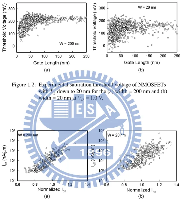
Figure 1.2: Experimental saturation threshold voltage of NMOSFETs with Lg down to 20 nm for the (a) width = 200 nm and (b)
width = 20 nm at VD = 1.0 V.
Figure 1.3: Experimental Ion-Iof f characteristics of NMOSFETs with
Lgdown to 20 nm for the (a) width = 200 nm and (b) width
= 20 nm at VD = 1.0 V. The Ionwas normalized against the
4 Chapter 1 : Introduction
Gate lengths of scaled MOSFETs are now under 30 nm in 45-nm node high-performance circuits [5,40-43]. Transistor scaling down to sub-20 nm and even beyond has been widely noticed encountering much more challenges at short channel control than previous gener-ations. The worsened short channel control enlarges electrical characteristic fluctuations, such as the deviation of threshold voltage, drive current, mis-match, and so on. Yield analysis and optimization, which take into account the manufacturing tolerances, model uncertainties, variations in the process parameters, etc., are known as indispensable com-ponents of the circuit design methodology [44-48]. Additionally, the fluctuation is intrin-sically increased with the scaling of transistor feature size, even not considering worsened short channel control [15,20-27]. Figure 1.1 shows the major sources of intrinsic parameter fluctuations, including the gate length deviation [15, 27, 36, 57-61], line edge roughness [15, 27, 36, 57-61], and random dopant fluctuation [21-27,62-89]. The fluctuation caused by granularity of the poly-silicon gate [90-93], silicon film thickness variation [94,95], and random telegraph signal [96,97] are also important factors in device intrinsic fluctuation, which dependents on the device structure. Figures 1.2 and 1.3 show the experimental
Vth fluctuation and the on- and off-state currents (Ion-Iof f) characteristics of the n-typed
MOSFETs (NMOSFETs) down to 20 nm gates. The gate length Lg values in Fig. 1.2 are
estimated from the gate capacitances in analysis data, and we presume the widths of all samples in Figs. 1.2(a) and 1.2(b) are 200 nm and 20 nm, respectively. As expected, the
1.2 : Vertical Channel Transistor Architecture 5
σVth roll-off characteristics of 20-nm-wide devices are much more scattered than that of
200 nm-wide devices. Notably, in Fig. 1.2, the maximum Vth difference for 20-nm-gate
length device has approached 150 mV, which is larger than the desired Vth, 140 mV. The
Ion-Iof f characteristic fluctuation becomes even worsened in Fig. 1.3. The maximum Vth
difference for 20-nm-gate length device is over 250 mV; moreover, in some cases, their Vth
are zero and can not be used in circuits and systems.
1.2 Vertical Channel Transistor Architecture
As the gate lengths of MOSFETs scales below sub-30 nm, the Field effect transistors (FETs) with multiple-gate structures, such as fin-type FETs (FinFETs) have been of great interest due to the excellent controlling ability of carriers in the device’s channel, which suppressed the short-channel effect [15-17]. The succession of device structure from pla-nar to vertical channel transistors has become the main trend in VLSI technologies. Fig-ure 1.4 plots an evolution of transistor architectFig-ure from planar MOSFETS to ultra-thin-body silicon-on-insulator (UTB SOI), double-gate, omega gate, and nanowire FinFETs. The transistors with vertical channel are with large gate-to-channel coverage ratio and have very thin body to control short-channel-effect.
6 Chapter 1 : Introduction
Figure 1.4: The evolution of transistor architecture from planar MOSFETs to ultra-thin-body silicon-on-insulator, double-gate, omega gate, and nanowire FinFETs.
1.2 : Vertical Channel Transistor Architecture 7
1.2.1 FinFET Process Steps
This section presents the manufacturing process of 25-nm-gate FinFETs. The process result is exhibited. The process simulation is similar to the sub-10-nm-gate nanowire FinFETs in [15-17,20], which is the state-of-art nanowire FinFETs transistor. The process flow used in this work is summarized:
1. Si fin and STI patterning, Tsi trimmed down upon STI etching;
2. Well and threshold voltage implantation; 3. Gate oxide growth (physical thickness 1.4 nm); 4. Gate deposition (in-situ doped N+poly silicon);
5. Poly Si chemical mechanical polishing;
6. Gate hard mask deposited and patterning (Hard mask trimmed down upon etching); 7. Poly gate etching;
8. Pocket and lightly doped drain (LDD) implantation; 9. Oxide/Nitride combo spacer formation;
10. Source/Drain implant;
11. Low-thermal-budget activation process; 12. Contact formation; and
13. Copper interconnect.
After Si fin patterning and shallow-trench isolation (STI) formation, the device width is trimmed down upon STI etching. Well and threshold voltage implantation are performed
8 Chapter 1 : Introduction
to adjust threshold voltage (Vth) of transistor. Then, to relieve the etch damage, a sacrificial
oxide is removed before gate oxidation. Thermal oxide is grown and in-situ heavily doped N+ poly-silicon is deposited. After the deposition and trimmed down of gate hard mask,
the pocket and lightly doped drain (LDD) implantation techniques are used for the suppres-sion of the short channel effect and hot carrier effect. Composite spacer of silicon oxide and nitride is deposited and etched anisotropically. After the gate and spacer formation, heavily doped N+junction are made with Phosphorous implantation. Low-thermal-budget
activation process is used for dopant activation and control of doping profile. After inter-layer-dielectric deposition, wolfram is used for metal contact plugging and copper is used for interconnection. Finally, alloying anneal is performed. We notice that the narrow width device trimmed down upon STI etching and low-thermal-budget activation process are the critical steps in fabrication of nanoscale FinFET transistor.
1.2.2 Process Simulation Using TCAD
The process simulation of FinFET is presented by using TCAD simulator [134]. Figure 1.5 presents the simulation result. After the Si fin patterning, STI patterning, and trimming, a silicon fin with substrate are formed, as displayed in Fig. 1.5(a”). The dark brown region in Fig. 1.5(a) and white region in Fig. 1.5(a’) are SiO2. The doping concentration in this step
1.2 : Vertical Channel Transistor Architecture 9
Figure 1.5: The process simulation result for FinFETs. ((a)-(a”))The device structure after Si fin patterning, STI. The doping concentration in this step is background doping with 1.0×1015cm−3 boron concentration.((b)-(b”))After
Well/Vthimplantation and annealing, the dopants are
activated after thermal annealing. The fabrication process then goes to gate formulation, pocket and LDD
implantation. The gate oxide is formulated after the gate oxide growth ((c)-(c”)). ((d)-(d”))After spacer formation and source/drain implantation, the final device structure is shown.
10 Chapter 1 : Introduction
shows the doping concentration after the well and threshold voltage implantation. The dopants are activated after thermal annealing. The fabrication process then goes to gate formulation, pocket and LDD implantation. The gate oxide is formulated after the gate oxide growth, as shown in Fig. 1.5(c’). The structure of heavily doped poly-silicon gate is then constructed and displayed in Fig. 1.5(c). The results of spacer and final source/drain implantation are presented in Fig. 1.5(d)- 1.5(d”).
1.3 Current Research Status and Motivation
This section reviews the current status of research and problem. Then the motivation of this thesis is drawn. The problems is first addressed as below.
1. There have been many studies of the intrinsic parameter fluctuations, including the process variation [15,27,36,57-61], random dopant fluctuation [21-27,62-89], and poly-silicon gate [90-93] on planar MOSFETs. However, the studies of FinFETs fluctuation is not enough [15,23,27,55,84]. Moreover, the extensive exploration of multi-gate channel transistor as well as comparison with planar MOSFETs are lacked.
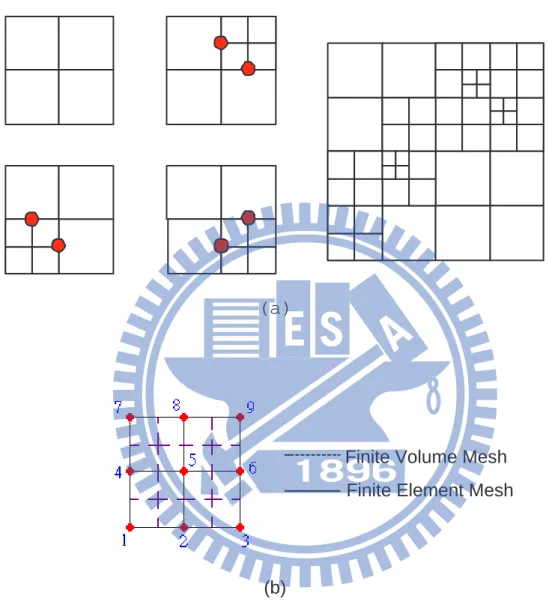
2. The use thin gate oxide becomes an important alternative research object [63] to fur-ther suppress the impact of fluctuation. Figure 1.6 shows the gate length deviation, line edge roughness, and random dopant fluctuation induced Vth fluctuation versus
1.3 : Current Research Status and Motivation 11
Figure 1.6: The gate length deviation, line edge roughness, and random dopant fluctuation induced Vthfluctuation versus equivalent
oxide thickness (EOT).
equivalent oxide thickness (EOT). The EOT reduction can be achieved by the in-troduction of metal-gate and high-κ dielectric for low standby power devices. All of the comparisons are based on the same off-sate (leakage) current. In principal, the standard deviation of Vth induced by the three aforementioned sources can all be
reduced with decreased gate dielectric thickness, due to less surface potential per-turbation under the enhanced gate controllability. This improvement will depend on implementation of reliable high-κ gate dielectrics and well work-function modulated
12 Chapter 1 : Introduction
metal gate.
3. High-κ/metal-gate technology has been recently recognized as the key to sub-45 nm transistor fabrication due to the small gate leakage current with an increased gate capacitance. Moreover, the sheet resistance is reduced with the use of metal as gate material. Comparing to the poly-gate technology, the metal-gate material will not react with high-κ material and therefore there existing less interface charge and Vth
pinning effect. The gate depletion in poly-gate material is no longer existed. Addi-tionally, the phono scattering effect is significantly reduced due to the less quantum resonance effect. However, the use of metal as a gate material introduces a new source of random variation due to the dependency of workfunction on the orientation of metal grains [121,122]. The grain orientation of metal is uncontrollable during growth period.
4. The use of vertical channel transistor to suppress the intrinsic parameter fluctuation is crucial. Figure 1.7 reviews the threshold voltage (Vth) fluctuation versus technology
node [15]. At 32-nm node, the thinner gate dielectric thickness could be achieved by the introduction of metal gate (for eliminating poly depletion) and high-κ (for thinner equivalent-oxide thickness but not increasing gate leakage) materials. An-other opportunity is not scaling gate dielectric thickness but enhancing short channel control with SOI substrate. Special attention will be paid to thin-buried-oxide SOI [49]. At sub-22 nm node, planar SOI will no more be a good device option, because
1.3 : Current Research Status and Motivation 13
Figure 1.7: The threshold voltage fluctuation versus technology node.
very thin body (less than 10 nm) is necessary for SCE control but meanwhile the thin body will degrade drive current due to ”quantum confinement” [50]. Then non-planar transistors such as FinFETs may emerge instead [51-56]. Their Vthfluctuation
characteristics should be addressed as well.
5. So far the most of aforementioned works are focused on the fluctuation of DC char-acteristics, the investigation of device’s AC as well as circuit’s fluctuations are lacked [84-91]. Though several works have addressed the importance of device variability in circuit, the simulation approach uses the compact model, which can not capture
14 Chapter 1 : Introduction
the random-dopant-position induced fluctuation and may underestimate the influence of fluctuation.
To deal with the aforementioned problems, this work extensively study the FinFET vari-ability and its fluctuation on circuits by a statistically-sound 3D ”atomistic” coupled device-circuit simulation approach [64-67,115-118]. The impact of individual fluctuation sources, consisting of gate length deviation, line edge roughness, random-dopant-fluctuation, and workfunction fluctuation, on the device’s DC/AC and circuit’s timing/power/high-frequency characteristic fluctuations are explored. The dominant fluctuation source in each charac-teristics are found. For the device characteristic fluctuations, the ”atomistic” simulation approach is effective to capture not only the randomness of doping concentration but also the random placement of dopants induced device variability. Moreover, a statistic simu-lation approach is applied to characterize the emerging workfunction fluctuation induced variability. The physical model of devices has been calibrated with experiential data [15-17,63]. To accurately describe the device variability in circuits, the circuit characteristics fluctuation are obtained by solving the both device transport and circuit nodal equations (so it’s called coupled device-circuit simulation). Unlike the compact model simulation approach, the coupled device-circuit simulation approach solves the device transport char-acteristics in circuit simulation and therefore provide the most device physics inside circuit
1.4 : Outline 15 fluctuation. The extensive study assesses the fluctuations on circuit performance and relia-bility, which can in turn be used to optimize nanoscale MOSFET and circuits.
1.4 Outline
This dissertation is organized as follows. Chapter 2 shows the used device model and nu-merical methods. The quantum-mechanical corrected transport equations and nunu-merical simulation methods are introduced, where a nanoscale FinFET is used as an example for simulation and calibration. Chapter 3 introduces the computer characterization technique for studying the effect of intrinsic parameter fluctuations including process-variation-effect (PVE), random dopant fluctuation (RDF), and workfunction fluctuation (WKF). The ac-curacy of characterization has been confirmed. Chapter 4 presents the random-dopant-induced characteristics fluctuation in vertical-channel transistors, where the impact of dis-crete dopant fluctuation on transistor physical and electrical characteristics are explored. This chapter also extensively explores the random-dopant-fluctuation in SOI transistors from single-gate to double-gate, triple-gate, and surrounding-gate transistor architectures. The effect of surrounding-gate coverage ratio on fluctuation resistivity is also discussed. Chapter 5 examines the impact of the intrinsic parameter fluctuations, PVE, RDF, WKF, in nanoscale FinFETs. The implications of device variability in circuits are explored in Chap-ter 6, in which the coupled device-circuit simulation approach is used instead of compact
16 Chapter 1 : Introduction
modeling approach for pursuing best accuracy. Finally, conclusions are drawn, suppression technique are prospected, and future work is suggested.
Chapter 2
Device Model and Numerical Methods
2.1 The Quantum-Mechanical Corrected Transport
Equa-tions
2.1.1 The Density-Gradient Equations
The technology computer-aided design (TCAD) simulations, such as process and device simulations, are widely used for the analysis of semiconductor devices. The process sim-ulation can generate the device geometry and doping profile according to the parameters of the fabrication processes. The output of process simulation is then used in the device simulation to estimate device characteristics. The drift-diffusion (DD) and hydrodynamic
18 Chapter 2 : Device Model and Numerical Methods
(HD) models play a crucial role in the development of semiconductor device simulator in the macroscopic point of view. The DD model was derived from Maxwell’s equation as well as charges’ conservation law and has been successfully applied to study device trans-port behavior, in the past decades. It assumes local isothermal conditions and is still widely employed in semiconductor device design.
Classical drift-diffusion model consists of at least three coupled partial differential equations (PDEs) for, such as electrostatic potential and electron-hole densities. When device channel is specified, a set of the DD equations in semiconductor device simulation is solved: 4φ = q εs (n − p + D), (2.1) 1 q 5 ·Jn= R(n, p), (2.2) and 1 q 5 ·Jp = −R(n, p), (2.3)
where φ is the electrostatic potential and its unit is volt. n and p are classical electron and hole concentrations (cm−3). q is the elementary charge and its unit is coulomb. The net
doping concentration is D(x, y, z) = ND+(x, y, z)−NA−(x, y, z). R is the net recombination rate (cm−3s−1). The carrier’s currents densities are given by
2.1 : The Quantum-Mechanical Corrected Transport Equations 19 and
Jp = −qµpp 5 φ − qDp5 p, (2.5)
where µnand µpare the carrier mobility (cm2/V − s). The diffusion coefficients, Dnand
Dp(cm2/s), satisfy the Einstein relation.
The quantum mechanical effects should be considered in the device simulation when the dimensions of the devices shrunk into nanometer scale. Various theoretical approaches have been presented to study the quantum confinement effects, such as full quantum me-chanical model (e.g. nonequilibrium Green’s function) and quantum corrections to the clas-sical drift-diffusion (DD) or hydrodynamic (HD) transport models. A set of Schr¨odinger-Poisson (SP) equations has been applied to study the quantum confinement effect in the inversion layers as well as the quantum transport between source and drain, but it is a time-consuming task in the TCAD application to realistic device characterization. Therefore, various quantum correction models, density gradient (DG) [99-103], H¨ansch[104], mod-ified local density approximation (MLDA)[105], effective potential (EP)[106-108], and unitfied quantum correction Model[109], have been proposed for classical DD or HD trans-port models. In this investigation, the density gradient was coupled with the DD model and solved for the quantum mechanical effects. The density gradient equation can be expressed as,
20 Chapter 2 : Device Model and Numerical Methods
~
Jn= −qµnn 5 φ + qDn5 n − qnµn5 γn, (2.6)
~
Jp = −qµpp 5 φ − qDp5 p + qpµp5 γp, (2.7)
where γn and γp are the quantum potentials for electrons and holes. γn = 2bn5
2√n
√ n .
γp = 2bp5
2√p
√p bn and bp are density-gradient coefficients for electrons and holes. bn =
~2/(12qm∗
n) and bp = ~2/(12qm∗p). m∗nand m∗p are effective masses for the electrons and
holes. ~ is the Planck constant. bnand bp in Eqs. (2.6) and (2.7) are the density gradient
coefficient which determines the strength of the gradient effect in the electron and hole gas. The last term in the right hand side of Eqs. (2.6) and (2.7) are referred to as “quantum dif-fusion”, which makes the electron continuity equation has a fourth-order partial differential equation. Therefore, such an approach is highly sensitive to noise in the local carrier den-sity, and the methodology is highly important in cases of strong quantization. To calculate the numerical solution of the multidimensional density-gradient model, firstly we decou-ple the coudecou-pled partial differential equations (PDEs); approximated with the finite volume method over nonuniform mesh. The corresponding system of the nonlinear algebraic equa-tions is then solved with the monotone iteration methods. Iteration will be terminated and post-processes will be performed when the specified stopping criteria for inner and outer iteration loops are satisfied, respectively.
2.1 : The Quantum-Mechanical Corrected Transport Equations 21
2.1.2 The Mobility Model
According to Mathiessen’s rule [113,114], the mobility model used in the device simulation can be expressed as:
1 µ = D µsurf aps + D µsurf rs + 1 µbulk , (2.8)
where D = exp (x/lcrit), x is the distance from the interface and lcritis a fitting parameter.
The mobility consists of three parts: (1) the surface contribution due to acoustic phonon scattering, where Ni = NA + ND, T0 = 300 K, E is the transverse electric field normal
to the interface of semiconductor and insulator, B and C are parameters which based on physically derived quantities, N0 and τ are fitting parameters, T is lattice temperature,
and K is the temperature dependence of the probability of surface phonon scattering; (2) the contribution attributed to surface roughness scattering is µsurf aps = BE + C(Ni/N0)
τ
E1/3(T /T0)K,
where Ξ = A + α·(n+p)Nrefv
(Ni+N1)v , Eref = 1 V/cm is a reference electric field to ensure a unitless
numerator in µsurf rs, Nref = 1 cm−3 is a reference doping concentration to cancel the unit
of the term raised to the power v in the denominator of Ξ, δ is a constant that depends on the details of the technology, such as oxide growth conditions, N1 = 1 cm−3, A, α, and
η are fitting parameters; (3) and the bulk mobility is µbulk = µL(TT0)−ξ, where µL is the
22 Chapter 2 : Device Model and Numerical Methods
2.2 The Numerical Simulation Methods
In this section, we will introduce the adaptive numerical methods in the following dis-cussion. The implemented adaptive computing technique for semiconductor device sim-ulation is mainly based on Gummel’s decoupling method [114, 124, 125], FV approxima-tion [112, 126], Monotone iterative method [135, 136], a posteriori error estimaapproxima-tion [112], and an unstructure meshing scheme [111, 114, 124, 125]. This simulation methodology has recently been developed for different device simulation [112, 126, 127]. The Gummel’s de-coupling method controls an iterative loop over two or more coupled equations. It is used when a fully coupled method would use too many resources of a given machine, or when the problem is not yet solved and a full coupling of the equations would diverge.
2.2.1 The Gummel Decoupling Method
To explore the transport behavior of transistors, the five coupled PDEs are numerically solved with Gummel’s decoupling method. With a given initial guess (φ(0), n(0), p(0), γ
n(0), γp(0))
and for each Gummel’s iteration index g, g = 0, 1, . . ., we first solve the nonlinear Poisson equation as well as density-gradient-corrected quantum potential equations.
∆φ(g+1)= q εs (n(g)− p(g)+ D(x, y) + BT (φ(g+1))). (2.9) γn(g+1)= 2bn 52√n(g) √ n(g) . (2.10)
2.2 : The Numerical Simulation Methods 23
γp(g+1) = 2bp5
2pp(g)
p
p(g) . (2.11)
The nonlinear Poisson equation is solved for φ(g+1), γ
n(g+1), and γp(g+1)given the previous
states n(g) and p(g). The quantum-corrected current continuity equation of electron is then
solved for n(g+1)with now the known functions φ(g+1), p(g), γ
n(g+1), and γp(g+1). 1 q∇ · (−qµnn (g+1)∇φ(g+1)+ qD(g+1) n ∇n(g+1)− qn(g+1)µn5 γn(g+1)) = R(n(g+1), p(g)). (2.12) Finally, we solve the quantum-corrected current continuity equation of hole with known
φ(g+1), n(g+1), γ n(g+1), and γp(g+1) 1 q∇ · (−qµpp (g+1)∇φ(g+1)− qD(g+1) p ∇p(g+1)+ qp(g+1)µp5 γp(g+1)) = −R(n(g+1), p(g+1)) (2.13) for p(g+1)until all preset stopping criteria are satisfied. Equations (2.9), (2.12), and (2.13)
are associated with proper boundary condition, respectively. We note that Eqs. (2.9), (2.12), and (2.13) are now three individual semilinear PDEs to be solved for each Gummel’s itera-tion. An outer iteration in the procedure of device simulation is then defined by Gummel’s decoupling method. We note that analysis of Gummel’s decoupling method in device simu-lation have been reported [110,112,114,124–128,130]. Then we can solve each decoupled PDEs with adaptive computing technique.
24 Chapter 2 : Device Model and Numerical Methods
The Gummel’s decoupling method Begin
While φ, n, and p in outer loop (Gummel’s loop) are not convergent If φ is convergent
Solve the nonlinear Poisson equation as well as density-gradient-corrected quantum potential by adaptive computing technique. End If
If n is convergent
Solve the quantum-corrected current continuity equation of electron with adaptive computing technique.
End If
If p is convergent
Solve the quantum-corrected current continuity equation of hole with adaptive computing technique.
End If End While
Call for next calculation.
2.2 : The Numerical Simulation Methods 25
2.2.2 The Adaptive Finite Volume Method
The discretization of semiconductor is performed based on adaptive 1-irregular mesh, tri-angular mesh, and finite volume (FV) approximation. The finite volume method is a nu-merical method for solving PDEs. It calculates the values of the conserved variables across the volume. Before using adaptive finite volume method to solve Poisson equation, we must understand the follow steps:
(1) Weak Formulation transforms into weak problem; (2) Discretize the simulation area by one-irregular mesh; (3) Form equation “Ax=B” by using FV method; and (4) Error estimation and mesh refinement.
The discretized step divides into structured mesh and unstructured mesh. If according to geometry, it divides into rectangle mesh and triangle mesh. But the rectangle mesh is easier to build than the triangle mesh. The one-irregular method is shown in Fig. 2.1. Figures 2.2(a) and 2.2(b) are the discretization scheme by finite volume method and finite element method, respectively. The initial mesh contains 25 nodes and then refined based on the estimation of solution error element by element. Notably, the process of mesh re-finement is guided by the result of error estimation automatically. As shown in plots, at the refinest level most of refined meshes are intensively located near the surface of channel and the junction of the drain side due to large variation of the solution gradient.
26 Chapter 2 : Device Model and Numerical Methods
(a)
Finite Volume Mesh Finite Element Mesh
(b)
Figure 2.1: The plot of FV method. (a) One-Irregular mesh, and (b) the difference between finite element mesh and finite volume mesh.
2.2 : The Numerical Simulation Methods 27
Figure 2.2: The mesh used for the solution process. Illustrations of MOSFET source/drain junction discretization. The p/n junction is discretized by (a) adaptive finite volume method and (b) adaptive finite element method.
28 Chapter 2 : Device Model and Numerical Methods
2.2.3 The Monotone Iterative Method
In previous subsection, we apply a finite volume method with nonuniform mesh technique to discretize the above PDEs in each directions. Using the divergence theorem on a finite hexahedral volume and considering the tensor-product meshes for the hexahedral volume, the discretized Poisson equation can be written as
ξi+1,j,kφi+1,j,k + ξi−1,j,kφi−1,j,k+ ξi,j+1,kφi,j+1,k+ ξi,j−1,kφi,j−1,k
+ξi,j,k+1φi,j,k+1+ ξi,j,k−1φi,j,k−1+ +ξi,j,kφi,j,k
= τi,j,k " qni εsi µ exp µ φi,j,k VT ¶ − exp µ −φi,j,k VT ¶¶ − q ¡ N+ D − NA− ¢ i,j,k εsi # , (2.14) where the arranged coefficients ξi,j,kand τi,j,kfor all i, j, and k are direct results from the
in-tegral approximations with the quadrature rule. After employing the boundary conditions, the above set of equations for the approximations φi,j,kat the nodes Xi,j,k = (xi, yj, zk) can
be written together as the compact matrix form,
AΦ = −B (Φ) . (2.15) Φ is the unknown vector formed by φi,j,k in the natural ordering, B is the vector of
non-linear functions corresponding to the finite volume discretization of equations. The matrix A is a seven-banded block-tridiagonal form. We note all coefficients in Eq. (2.14) are nonnegative and the following relation:
![Figure 1.1: The major sources of intrinsic parameter fluctuations: the gate length deviation, line edge roughness, and random dopant fluctuation [15].](https://thumb-ap.123doks.com/thumbv2/9libinfo/8228458.170823/39.892.94.756.469.859/figure-sources-intrinsic-parameter-fluctuations-deviation-roughness-fluctuation.webp)