國
立 交 通 大 學
電信工程學系
博 士 論 文
高頻、高品質因素
及低相位雜訊壓電振盪器之研究
Investigation of High Frequency,
High Quality Factor and Low Phase Noise
Oscillators with Piezoelectric Resonators
研 究 生:林炯宏
指導教授:高曜煌
高頻、高品質因素及低相位雜訊壓電振盪器之研究
Investigation of High Frequency, High Quality Factor
and Low Phase Noise Oscillators with Piezoelectric
Resonators
研究生:林炯宏
Student:
Jon-Hong
Lin
指導教授:高曜煌 博士 Advisor:
Dr.
Yao-Huang
Kao
國立交通大學
電信工程學系
博士論文
A Dissertation
Submitted to Institute of Communication Engineering
College of Electrical and Computer Engineering
National Chiao Tung University
in Partial Fulfillment of the Requirements
for the Degree of Doctor of Philosophy
in
Communication Engineering
Hsinchu, Taiwan
高頻、高品質因素及低相位雜訊壓電振盪器之研究
學生:林炯宏
指導教授
:高曜煌 博士國立交通大學電信工程學系博士班
摘
要
在高速數位通訊系統中,為解決不同傳輸速率設備間訊號之連結與訊號在長
距離傳輸後之衰減,系統之寬頻收發器須具備時脈恢復電路對訊號作頻率轉換及
波形重整以維持資料完整性。上述電路中均須使用高性能之壓控振盪器,因此具
高穩定性之高品質因素壓控壓電振盪器成為最佳選擇。若以壓電共振器的製程限
制及工作頻率來區分,當工作振盪頻率低於
200 MHz 時,石英晶體共振器為最
佳選擇;當工作頻率低於
3000 MHz 時,表面聲波共振器(SAWR)為目前主流元
件;而薄膜體波共振器(FBAR)則適用於微波頻段。
本論文共提出四種高品質因素壓電振盪器,分別為: 2488 MHz 壓控聲橫波
(STW)振盪器,2488 MHz 壓控薄膜體波(FBAR)振盪器,622 MHz 修正式皮爾斯
(Pierce)振盪器及 433 MHz 平衡式表面聲波(SAW)振盪器。
本文中
2488 MHz 壓控聲橫波振盪器之可調頻率範圍可達±200 ppm,其相位
雜訊在
100 kHz 偏移時,相較於一般市售同類產品低 8 分貝;在振盪器設計階段
藉由分析元件的殘餘相位雜訊(residual phase noise),發現聲橫波共振器為本振盪
器主要雜訊來源,而非主動元件。振盪器之相位雜訊可經由元件之殘餘相位雜訊
及回路轉換函數預測且預測值與量測結果相當接近。本
2488 MHz 壓控薄膜體波
振盪器之可調頻率範圍可達±6%,其振盪頻率之溫度係數大約為-34.5 ppm/
oC。
我們藉由在傳統皮爾斯振盪器之回授
π 電路上增加一相移器來降低回授電路
+1.2V, 10.2 mA,其相位雜訊在距中心載波 10 kHz 處可達-136 dBc/Hz。
我們藉由一般商用表面聲波共振器來製作平衡式表面聲波振盪器,其對偶特
性經由量測獲得驗證,並增加一
180 度反相功率偶合器來完成 push-push 架構振
Investigation of High Frequency, High Quality
Factor and Low Phase Noise Oscillators with
Piezoelectric Resonators
Student:Jon-Hong Lin
Advisors:Dr. Yao-Huang Kao
Institute of Communication Engineering
National Chiao Tung University
ABSTRACT
The increasing demand for high speed digital communication applications
motivates a growing interest in the high data rate transceivers. In these transceivers,
clock recovery circuits are used for data integrity. The clock is usually extracted from
a phase-lock-loop circuit with low phase noise voltage-controlled oscillator (VCO).
For the requirements on the high frequency and low phase noise voltage-controlled
oscillators, the highly stable VCOs with piezoelectric resonators are the hopeful
candidates. In the frequency below 200 MHz, the crystal resonators are the best choice.
In the ultar-high-frequency (UHF) band, surface acoustic wave resonators (SAWR)
play the important roles now. In the band of UHF and microwave frequency, the film
bulk acoustic resonators (FBAR) are the future stars. There are four different types
oscillators are presented in this thesis. They are VCO with STW resonator, VCO with
FBAR, modified Pierce SAW oscillator, and balanced SAW oscillator.
Both the surface transverse wave (STW) resonator and FBAR are applied for the
low phase noise 2488 MHz voltage-controlled oscillators. The tuning ability of the
2488 MHz voltage-controlled oscillator with STW resonator achieves ±200 ppm and
its phase noise performance is 8 dB better than the other commercial products at offset
100 kHz frequency. The white phase-noise floor is about -170 dBc/Hz. In the design
phase of the oscillator with STW resonator, by examining the residual phase noises of
the main components in the oscillator, we found that the STW resonator dominates the
phase noise of the oscillator, instead of active devices. The behavior of the phase
noise of the oscillator is shaped by the important factor of group delay. The tuning
capability of the voltage-controlled FBAR oscillator achieves ±6%. The temperature
coefficients factor is about -34.5 ppm/
oC which is dominated by FBAR.
An extra phase shifter is used to reduce the insertion loss of the π-feedback
network in the conventional Pierce SAW oscillator. The modified Pierce oscillator
provides 4.0dBm of output power and the core circuit consumes 10.2 mA from +1.2V
DC power supply. The phase noise level of the oscillator is approximately –136
dBc/Hz at 10 kHz offset.
With a popular commercial one-port SAW resonator, the behavior of the balanced
SAW oscillator is presented. The balanced SAW oscillator provides pure antiphase
signals without balun. By using an 180
opower combiner, a push-push topology SAW
oscillator is presented and results in 6dB phase noise improvement in comparison with
the single-end output.
誌
謝
長時間在職場工作後,心中漸漸有被掏空的感覺,體會到再進修的必要,在
內人的支持下暫別職場來到交大。非常感謝高曜煌教授這幾年的指導與教誨,除
學習高頻電路及積體電路的知識外,還有機會一窺壓電振盪器設計的堂奧。學習
的過程雖然艱辛,也充滿了挑戰與挫折,但在師長及同學的陪伴協助下,最終否
極泰來,心靈與知識也在磨練中更上一層樓。
我要感謝立朗科技、台灣晶技、台灣嘉碩及希華晶體等幾家公司在我求學期
間所提供的表面聲波元件、製程及量測設備,尤其要感謝吳朗教授讓我在立朗科
技任職期間能有機會以材料的觀點來重新認識壓電材料特性及表面聲波元件。同
時要感謝
Dr. B. Temple (Agilent Technology, Spokane, WA) 協助驗證量測系統及
比對振盪器量測結果並提供相當多有關雜訊量測的寶貴經驗。
我還要感謝國家晶片中心(CIC)提供晶片設計及製作的環境,讓晶片能順利製
作完成;並感謝中科院提供的
FBAR 的設計、量測與製程,讓我有機會接觸到
FBAR 並完成壓控振盪器的製作。
最後,我要感謝一直在背後默默支持的內人,沒有她的支持,我就沒有辦法
順利完成學業。並在此衷心祝福所有陪伴我走過求學之路的師長、同學及朋友。
林炯宏
書於風城
2009 年 1 月
目
錄
中文摘要
………..……… i
英文摘要
………..……… iii
誌謝
………..……… v
目錄
………..……… vi
表目錄
………..……… viii
圖目錄
………..……… ix
Chapter 1
Introduction………...……….………
1
1.1
Motivation……… 1
1.2
Feedback Loop Oscillators with Piezoelectric Resonators……..
3
1.3
Modified Pierce Oscillator with One-port SAW Resonator……
4
1.4
Balanced Oscillator with One-port SAW Resonator………...…
5
1.5
Organization of this thesis………...
5
Chapter 2
Feedback Loop Oscillators with Piezoelectric Resonators….
7
2.1 Piezoelectric
Resonators…..………
7
2.1.1 SAW
Resonators.………. 7
2.1.2 Film
Bulk
Acoustic Resonators...………
9
2.2 Voltage-Controlled
Oscillator
with STW Resonator…...………
13
2.2.1 Design
Method………. 13
2.2.2 STW
Resonator……… 14
2.2.3 Loop
Amplifier……… 18
2.2.4 Power
Splitter……….. 18
2.2.5 Electronic
Phase
Shifter………... 19
2.2.6 Oscillator
Performance……… 20
2.3 Voltage-Controlled
Oscillator
with FBAR Resonator…….……
25
2.3.1
FBAR Design and Fabrication……….
26
2.3.2 Oscillator
Design………. 31
2.3.3
Measurement and Discussion………..
33
Chapter 3
Measurement and Prediction of Phase Noise in Oscillator
with STW Resonator……..………....…
36
3.1 Introduction………..
36
3.2
Residual Phase Noise of Devices……….
37
3.2.1 Residual
Noise………. 37
3.2.2
Measurement Process of Residual Phase Noise……...…………
39
3.2.3
Residual Phase Noise of Main Components in Oscillator……...
41
3.3
Absolute Phase Noise of Oscillators………
44
3.3.1
Phase techniques of absolute phase noise measurements………
45
3.3.2
Theory of FM discriminator……….
48
3.3.3
Frequency Discriminator System Setup………...
51
Chapter 4
Modified Pierce Oscillator with One-port SAW Resonator..
58
4.1 Introduction………..………
58
4.2
One-port SAW Resonator………
59
4.3 Oscillator
Design……….………
60
4.4 Oscillator
Performance………
68
Chapter 5
Balanced Oscillator with One-port SAW Resonator…...…
72
5.1 Introduction………..………
72
5.2 Oscillator
Design……….………
72
5.3
Measurement and Discussion………..………
77
Chapter 6
Conclusions.……… 84
表 目 錄
2.1
Measured results for the voltage-controlled STW oscillator and
comparison with the other commercial products.………..……
23
2.2
Physical properties of representative materials for FBAR..……
27
2.3
Measured results for the FBAR oscillator………...…
33
4.1
Measurement results for the SAW oscillator…….………..
68
5.1
Parameters of the transistor………..………
74
5.2
Performance of balanced SAW oscillator………..…………..…
77
5.3
Harmonics before and after the 0
oor 180
opower combiner……
82
圖 目 錄
1-1
Frequency translation circuit………..………...
3
1-2
Clock recovering circuit…………..………..………
4
2-1
(a) Structrue, and (b) equivalent circuit model for one-port
SAW resonator………..………...……
8
2-2
(a) Structrue, and (b) equivalent circuit model for two-port
SAW resonator………..………...
9
2-3
Thin film resonator configurations (a) membrane formed by
etching a VIA in the substrate. (b) air gap isolated resonator.
(c) solidly mounted resonator (SMR) using a reflector array to
isolate the resonator from the substrate………...
10
2-4
Butterworth Van Dyke (BVD) equivalent circuit………
12
2-5
Block diagram of a feedback loop oscillator………...
14
2-6
(a) Picture, and (b) structure of the STW Resonator, (c)
insertion loss from 2468 to 2508 MHz, and (d) insertion loss
and transmission phase responses 2486.32 - 2490.32 MHz…....
16
2-7
Wilkinson power splitter……….……….………... 18
2-8
Electronic phase shifter………... 19
2-9
Total phase shifter and the open loop gain at the oscillation
frequency………..
20
2-10
(a) Measured output spectrum for the 2488.32 MHz and (b)
harmonics spectrum……….…
21
2-11
Dependence of the oscillation frequency on tuning voltage....…
22
2-12
Dependence of the oscillation frequency on temperature……....
23
2-13
Measured phase noise spectrum for the oscillator with STW
resonator………...
24
2-14
Process flow of FBAR…..………... 27
2-15
Picture for the film bulk acoustic resonator.………
29
2-16
Cross-sectional SEM photograph of (002)-oriented AlN film
with SiN
Xbuffer layer (a) 30000X, (b) 60000X....………..
29
2-17 Z-parameters
of
the FBAR…...………
31
2-18
Block diagram of a feedback loop oscillator………...
32
2-19
Results of linear simulation using ADS………...
32
2-20
(a) Output fundamental spectrum, and (b) harmonics spectrum
for the oscillator………...
34
2-21
Measured variation of fundamental frequency with temperature
for FBAR and oscillator……….………..
35
2-22
Output frequency vs. tuning voltage...………...
35
3-1
Additive noise component.…..………
38
3-2
Multiplicative noise component..……...……... 38
3-3
The basic setup for residual phase noise measurement………...
40
3-4
The E5503B connection diagram for residual phase noise
measurement………...……….
40
3-5
Measured noise floor for residual phase noise measurement
system………..
41
3-6
Residual phase noise of STW resonator………..…………....…
42
3-7
Residual phase noise of loop amplifier………....
43
3-8
Residual phase noise of electronic phase shifter…...…………...
44
3-9
General block diagram described in NIST technical note
1337………..
46
3-10
Basic block diagram for frequency discriminator…...………….
48
3-11
Connect diagram of Agilent E5503B for FM discriminator
technique……...
52
3-12
The measured system noise floor and the null points for FM
discriminator………
53
3-13
Measured phase noise for the 2488.32 MHz STW oscillator…..
54
3-14
The open loop gain and phase shift of the STW oscillator at the
oscillation frequency………
55
3-15
Transfer functions in open loop circuit………...
55
3-16
The transfer function vs. Fourier frequency……….…………...
57
4-1 Conventional
Pierce
oscillator...….………. 58
4-2
Equivalent circuit for SAW resonator…….………
60
4-3 Reactance
of
SAW
resonator………... 60
4-4
Phase shift and insertion loss of open-loop simulation for
conventional Pierce oscillator……..………
62
4-5
Modified pierce oscillator…….………... 63
4-6
Phase shift and insertion loss of open-loop simulation for
Modified Pierce oscillator…...………….………
63
4-7
The ABCD matrix for T-circuit………..………. 65
4-8
The ABCD matrix for π-circuit……….………... 65
4-9
The 90 degree phase shifter at 622.08 MHz………..…………..
65
4-10
Circuit diagram of active device of SAW oscillator.…………...
66
4-11
Results of linear simulation using ADS………...
67
4-12
Picture of the active part of the SAW oscillator………..
68
4-13
(a) Fundamental spectrum, and (b) harmonics spectrum of
oscillator………...
69
4-14
Phase noise comparison for different SAW oscillators………...
70
5-1 Oscillator
with
one-port
SAW resonator…..………...
73
5-2 Equivalent
circuit
model
for one-port SAW resonator…………
73
5-3
Balanced Oscillator with one-port SAW resonator…..………...
75
5-4
Principle of push-push oscillator…….………
76
5-5
Photograph of balanced SAW oscillator………..
77
5-6
Circuit diagram of balanced SAW oscillator with ASK switch..
78
5-7
Measured output waveforms of the balanced SAW oscillator….
79
5-8
Harmonic spectrum of the output Q+………..
80
5-9
Harmonic spectrum of the output Q-………...
80
5-10
Harmonic spectrum of the subtraction (Q+, Q-)……….……….
81
5-11
Harmonic spectrum of the sum (Q+, Q-)….………
81
5-12
Measured phase noise of SAW oscillator at 433 MHz……...….
83
Chapter 1
Introduction
1.1 Motivation
The increasing demand for high speed wire (or wireless) communication applications, such as optical communications, cellular phone, wireless data networks, global positioning systems, etc., motivates a growing interest in the high data rate transceivers. In these transceivers, clock recovery circuits are used for data integrity. The clock is usually extracted from a phase-lock-loop circuit with low jitter voltage-controlled oscillator (VCO). For the requirements, the highly stable VCOs with piezoelectric resonators are the hopeful candidates.
In a benchmark letter [1], D. B. Leeson summarized the phase noise characteristics of the oscillator which is form by cascading the amplifier with a resonator and closing the loop. The expression for oscillator single side band noise from Leeson is ⎥ ⎥ ⎦ ⎤ ⎢ ⎢ ⎣ ⎡ ⎟⎟ ⎠ ⎞ ⎜⎜ ⎝ ⎛ + ⎟ ⎟ ⎠ ⎞ ⎜ ⎜ ⎝ ⎛ ⎟⎟ ⎠ ⎞ ⎜⎜ ⎝ ⎛ + = S m c m l m P FkT f f f Q f f 1 2 1 2 1 log 10 ) ( L 2 0 (1.1) Where l
Q = loaded quality factor of the resonator
F = effective noise factor
PS = signal level at the oscillator active element input
fm = offset frequency
fc = flicker frequency
f0 = center frequency k = Boltzmann’s constant
According to Leeson’s model above, we can find the parameters which includeQ , Pl S, F , and fc are important when designing the low phase noise oscillator.
For low phase noise design, the piezoelectric resonators which normally have high quality factor are chosen as the tanks of the oscillators in UHF band.
The existence of the surface acoustic wave (SAW) was first discussed in 1885 by Lord Rayleigh. [2] Till 1965, White suggested that SAWs can be excited and detected efficiently by using an inter-digital transducer (IDT) placed on the piezoelectric substrate. [3] This is because very fine IDTs can be mass-produced by using photolithography, which has been well developed for semiconductor device fabrication, and proper design of the IDT enables the construction of transversal filters with outstanding performance. [4] The width of the IDT is proportional to the velocity of the acoustic wave. The wave velocity and the resolution of the photolithography are the important limits for the mass production SAW devices. For example, quartz is widely used to fabricate the resonators for use in stable oscillators because of its low temperature coefficient. The wave velocity in quartz is about 3100 m/s for Rayleigh wave mode. The width of the IDT which is about quarter wavelength of acoustic wave will be as fine as 0.31μm for 2500 MHz SAW devices. This width is much smaller than the resolution of photolithography which is about 0.5μm for mass production SAW devices. [5] It needs high investments in the fabricated equipments to achieve this resolution. So, several higher wave velocity materials and wave modes are developed in recent years. Here, we present four types of oscillators for different piezoelectric resonators application. They are 2488 MHz voltage-controlled oscillator with surface transverse wave (STW) resonator, 2488 MHz voltage-controlled oscillator with film bulk acoustic resonator (FBAR), 622 MHz modified Pierce oscillator with one-port SAW resonator, and balanced oscillator with one-port SAW resonator.
1.2 Feedback Loop Oscillators with Piezoelectric Resonators
For Synchronous Optical Network (SONET) Optical Carrier level 12 (OC-12) applications, the VCOs were mostly fabricated at 622 MHz either by the fourth harmonic of 155 MHz crystal oscillator (VCXO) or directly 622 MHz SAW oscillator (VCSO). For OC-48 applications which are shown in Fig. 1-1 and Fig. 1-2, due to the availability of high frequency and high quality resonator, the VCOs were mostly fabricated at 2488 MHz by the fourth harmonic of 622 MHz SAW oscillator (VCSO). [6, 7] But it will suffer from the degradation factor of 20log N =12dB on the phase noise as applications to OC-48. Seldom studies on 2488 MHz have been presented. [8-10] To fulfill this requirement, the STW resonator and the FBAR working directly at 2488.32 MHz are developed for the tanks of the VCOs.The high-Q STW resonator on quartz was demonstrated in 1987 [11]. Its advantages over the conventional Rayleigh waves are the very high velocity and low propagation loss [4]. The wave velocity of STW is approximately 5000m/s. High wave velocity makes the width of IDT larger and then reduces the requirement of the photolithography process. A coupled-mode resonator with unloaded Q = 5500 has been carefully designed to accommodate the request of wide band tuning and low phase noise applications. By using this STW resonator, a STW resonator based oscillator was developed in response to SONET OC-48 application.
Loop Filter
÷4
VCO
622MHz Freq. & Phase Detector 2488MHz
Loop
Filter VCO
Freq. & Phase
Detector 2488MHz
2488MHz
Fig. 1-2 Clock recovering circuit.
After the success on the development of 2488 MHz voltage-controlled oscillator with STW resonator, we try to use the FBAR to replace the STW resonator. Because the high investments in the fabrication equipments for the SAW resonator which working at the frequency above 2500 MHz, the FBAR is the hopeful candidate for the resonators used in microwave oscillators. A 2488 MHz FBAR based on AlN thin film process was developed for this work. By using this resonator, a FBAR based oscillator was developed in response to SONET OC-48 application.
1.3 Modified Pierce Oscillator with One-port SAW
Resonators
The Pierce oscillator is one of the more popular circuits for the crystal oscillator today. In comparison with feedback loop oscillator, the component counts of Pierce oscillator will be lower. While applying this circuit working with a one-port SAW resonator at UHF frequency, the shunting capacitance has a serious bad effect on the high frequency oscillation. The shunting capacitance increases the insertion loss of the π-feedback network in the Pierce oscillator which constructed by one-port SAW resonator and two capacitors. This feature makes the oscillator hard to start oscillation
and the efficiency to degrade. To prevent these disadvantages, we modified the conventional Pierce oscillator circuits by adding an extra phase shifter. This modification successfully solves the problem above.
1.4 Balanced Oscillator with One-port SAW Resonator
The balanced circuits are widely used to enhance the circuit’s performance, which like differential amplifier and balance mixer. The improvement of the circuit’s performance relies on the availability of the antiphase signal sources, which is often the difficult part of the circuit design. Traditionally, the antiphase signals are obtained by using passive or active balun. The balanced oscillator can provide the antiphase signals without balun. Several balanced oscillator circuits using different type resonators have been reported. [12-16] But the balanced oscillator with one-port SAW resonator is hard to find. Here, we use a popular 433 MHz one-port SAW resonator to present the circuit and discuss the behavior of the balanced SAW oscillator.
1.5 Organization of this thesis
It is the aim to investigate the problems while applying piezoelectric resonators to build the high frequency, high quality factor, and low phase noise oscillators and provide some useful solutions.
In chapter 2, the structure and equivalent circuits for SAW resonator and FBAR are introduced. By using these resonators, we present two feedback loop oscillators: 2488 MHz voltage-controlled oscillator with STW resonator and 2488 MHz voltage-controlled oscillator with FBAR. The designs of oscillators and performances will be measured and discussed.
noise of the two-port devices will be introduced. After that, we will discuss the different measurement techniques for absolute phase noise measurement and chose the frequency discriminator method to measure the phase noise of the oscillators with piezoelectric resonators. By examining the residual phase noise of the devices, we can find the main noise contributors in the oscillator quickly and accurately. The method to predict the phase noise of the feed-back loop oscillator based on the residual phase noise of devices will be introduced. The prediction of the phase noise of the oscillator has a good agreement with the measured results.
In chapter 4, Pierce oscillator which is widely used in low-frequency crystal oscillators is applied for 622 MHz application. For solve difficulty of the oscillation start-up in this band, an extra phase shifter is added. The oscillator design method and how to choose a proper phase shifter are discussed.
In chapter 5, the balanced oscillator with a 433 MHz one-port SAW resonator is presented. We use a commercial one-port SAW resonator which is made by ftech Co. to demo this circuit. Based on this balanced oscillator, a push-push SAW oscillator is constructed and achieves 6dB improvement in phase noise of oscillator in comparison with one-side oscillator.
In chapter 6, there are the short conclusion of our work and the view of the future work.
Chapter 2
Feedback Loop Oscillators with Piezoelectric
Resonators
2.1 Piezoelectric Resonators
2.1.1 SAW Resonators [4]
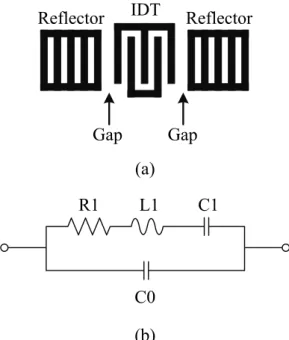
Both one-port and two-port SAW resonators are used for the tanks of oscillators in this thesis. Fig. 2-1(a) shows a typical configuration of the one-port SAW resonator where two grating reflectors are replaced at both ends of the inter-digital transducers (IDT). Very steep resonance can be detected by the IDT when the device is designed so that resonance frequencies of the IDT and reflectors coincide with each other. The width of the IDT is about quarter wavelength of the acoustic wave. The length of the gaps between the IDT and reflectors significantly influence the resonance characteristics. Fig. 2-1(b) shows the equivalent circuit near resonance, where C1 and L1 are the motional capacitance and inductance, respectively, corresponding to the contributions of elasticity and inertia. R1 is the motional resistance corresponding to the contribution of damping. C0 is the capacitance of the IDT. The capacitance ratio γ is given by: 1 1 1 0 2 − ⎟⎟ ⎠ ⎞ ⎜⎜ ⎝ ⎛ = = r a C C ω ω γ (2.1)
where ωr and ωa are the resonant frequency and anti-resonant frequency, respectively.
The smaller γ enable us to control the oscillation frequency over a wider range by a capacitance parallel-connected to the resonator. This feature is preferable for use in a voltage controlled oscillator where the varactors are employed as a voltage adjustable
capacitance. IDT Reflector Reflector Gap Gap (a) R1 L1 C1 C0 (b)
Fig. 2-1 (a) Structrue, and (b) equivalent circuit model for one-port SAW resonator.
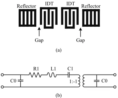
Fig. 2-2(a) shows a two-port SAW resonator where the grating reflectors are replaced at both sides of a conventional transverse filter. When the devices are designed so that the reflectors resonance at IDT resonance frequency, the transfer admittance becomes very large at resonance and a very narrow but low-pass passband is realized. Fig. 2-2(b) shows the equivalent circuit near resonance. The resonance circuit is involved as s shunt element between two IDTs because the structure is equivalent to a one-port SAW resonator when the two IDTs are parallel-connected. The oscillator can be constructed by using two-port SAW resonator as a feedback element. This configuration is widely used for operation in the UHF range because of its insensitivity to parasitic circuit elements.
IDT
Reflector IDT Reflector
Gap Gap
(a)
R1 L1 C1
C0 1:-1 C0
(b)
Fig. 2-2 (a) Structrue, and (b) equivalent circuit model for two-port SAW resonator.
2.1.2 Film Bulk Acoustic Resonators
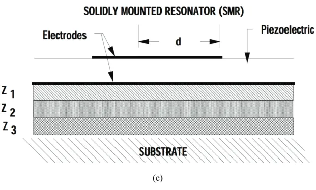
Another high frequency bulk wave approach is to obtain a specified thickness by thin film deposition techniques rather than by thinning crystal plates. There is considerable breadth to the thin film resonator technology, both in device types and applicable frequency spectrum. Much of this is due to the fact that the technology is based upon thin films that can be fabricated, by various means, on a variety of substrates employing integrate circuit type wafer scale processing. Bulk wave resonators require that both surfaces be free to vibrate, even though vibration amplitudes are fractions of a nanometer, in order to sustain a resonance. This condition is supplied by mechanically free surfaces such air or vacuum. Resonator geometries suitable for use with piezoelectric thin film resonators are shown in Fig. 2-3. The resonators in Fig. 2-3(a) and (b) have mechanically low impedance material interfaces of air or vacuum while the one in Fig. 2-3(c) is solidly attached to the substrate. The configuration of Fig. 2-3(a) is a membrane structure supported by the edge of the substrate [17-30].
(a)
(c)
Fig. 2-3Thin film resonator configurations (a) membrane formed by etching a VIA in the substrate. (b) air gap isolated resonator. (c) solidly mounted resonator (SMR) using a reflector array to isolate the resonator from the substrate.
Typical fabrication involves deposition of a piezoelectric film on a supporting substrate followed by removal of a portion of the substrate to form the membrane and thereby define the resonator. The configuration is similar to that used in inverted mesa quartz crystals where a thin piezoelectric membrane is surrounded by a more rigid supporting structure. The difference is in the details of how the membranes are formed. The second configuration involves fabricating an air gap under the resonator [31,32]. This may be accomplished by first depositing and patterning an area of temporary support material, next depositing and patterning an overlay piezoelectric resonator with electrodes, and finally removing the temporary support. The approach in Fig. 2-3(a) has seen greater work of the two membrane configurations and is know generally as the FBAR (Film Bulk Acoustic Resonator) configuration [19].
Advances in thin film processing have allowed the fabrication of membrane devices with high width to thickness ratios. Within one membrane of AlN multiple
resonators have been fabricated and electrically interconnected to form complex ladder filters [22]. Resonators have an electrical response that is modeled quite accurately by the Butterworth Van Dyke (BVD) equivalent circuit shown in Fig. 2-4. [23,27].
R1 L1 C1
C0
2.2 Voltage-Controlled Oscillator with STW Resonator
2.2.1 Design Method
In this section, a highly stable VCSO with STW resonator working directly at 2488.32 MHz is developed. The high-Q STW resonator on quartz was demonstrated in 1987 [11]. Its advantages over the conventional Rayleigh waves are the very high velocity and low propagation loss [4]. The wave velocity of STW is approximately 5000m/s, which relaxes slightly the requirement of the photolithography process. A coupled-mode resonator is carefully designed to accommodate the request of wide band tuning and low phase noise applications. The unloaded quality factor equal to 5500 was realized in this work.
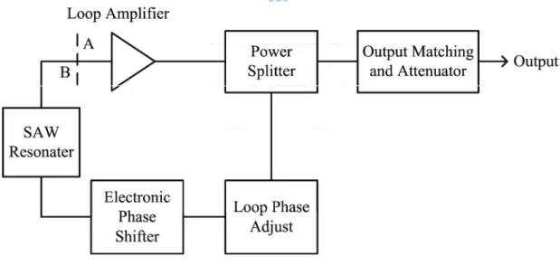
It is noted that the oscillator with one-port SAW resonator suffers from large parasitic capacitance from inter-digit transducers. Here, the architecture with two-port resonator forming a feedback loop is chosen as shown in Fig. 2-5. It consists of a single loop amplifier, an electronic phase shifter, a lump element reactive Wilkinson power splitter, a lumped element reactive phase adjusting, and a two-port STW resonator. The resonator acts as a short circuit with zero phase-shift at the desired frequency. No output buffer amplifier is used because it may degrade the oscillator’s white phase noise floor. The oscillation starts as the closed loop gain satisfies Barkausen’s criteria. The total loop gain is larger than unity at the frequency of oscillation and the phase shift is equal to 2πN radians, N is an integer. The conditions are written as
∑
(Ga,Gp,Gs)≥ 1 (2.2) and N s p a θ θ π θ + + =2 (2.3)where, Ga:Gain of Loop Amplifier, Gp:Loss of Phase Shifter and Loop Phase Adjust, Gs:Loss of STW Resonator, θa:Phase change in Loop Amplifier, θp: Phase change in Phase Shifter and Loop Phase Adjust, and θs:Phase change in STW Resonator. During design phase, the open loop gain is evaluated by breaking the loop at the appropriate plane with equal input and output impedance, such as line AB noted in Fig. 2-5. Here, the impedances seen are 50ohm network analyzer measurement. Actually the input/output impedances in each module are all set to 50ohm for convenience. This approach has the advantage that the noise characteristics of the individual component as measured in an open-loop configuration have a direct bearing on the closed-loop phase noise of the oscillator.
Fig. 2-5 Block diagram of a feedback loop oscillator.
2.2.2 STW Resonator
To achieve low insertion loss, high frequency, and high quality factor, the SAW resonator with STW is employed.[5] The picture of the resonator is shown as Fig. 2-6(a). The STW is a shear wave with very high velocity and energy trapping reduces the diffraction of the shallow bulk wave into the substrate, thus reduce in device
insertion loss and increase in resonator Q. The width of the transducer is approximately 0.5μm. The overlap aperture is about 250μm. This larger transducer width also makes it possible that the resonator could be manufactured in mass production with acceptable yield. Since STW also do not associate volume charge with propagation, its propagation loss is small. [4] To achieve the proper turnover temperature, the 90° rotated ST-cut quartz is employed to be as substrate of the resonator, which has the turnover temperature approximately at 45°C. This work simplifies the circuit design without using extra temperature compensation circuit for the real environment and lowers the cost.
The IDTs are detailed in Fig. 2-6(b) with die size of 1.8mm x 1.2mm. The input and output IDTs have 100 fingers are placed between two shorted reflectors, which has 90 fingers, and are separated by a shorted grating with 3 fingers. The resonant modes formed by input and output IDTs are coupled just as two coupled parallel LC resonators. The coupling is carefully tuned by the central grating. This results in a two-mode wideband response such as that shown in Fig. 2-6(d). Due to the grounding grating the insertion loss is reduced to 4~5dB, which is much smaller than that of 10~15dB in conventional SAW or STW delay line. [10] The approximately linear phase change with slope equal to 1.713×10⁻⁶rad/Hz is obtained within the 3dB frequency band. The up and down limits of the phase change are above ±90o. The loaded Q factor ω φ ω d d Q o L = ⋅
2 is estimated equal to 1537. The group delay is about 1.713×10⁻⁶ rad/Hz. High insertion loss out of the pass band is revealed in Fig. 2-6(c). The spurious are suppressed under 30dB. The center frequency is trimmed to 2488.32 MHz.
(a)
(c)
(d)
Fig. 2-6 (a) Picture, and (b) structure of the STW resonator, (c) insertion loss from 2468 to 2508 MHz, and (d) insertion loss and transmission phase responses 2486.32 - 2490.32 MHz.
2.2.3 Loop Amplifier
The HBT monolithic amplifier is selected as the loop amplifier because of low noise figure and high dynamic range. The P1dB is at +17dBm and the bandwidth is 4 GHz. Its bandwidth was properly selected to prevent high 2nd harmonics. The nominal gain of 17dB is much greater than that required to overcome the total loop losses to insure the stable oscillation. The magnitude of gain variation over temperature is approximately 0.005dB/°C and this feature can prevent the AM-PM noise induced with the temperature variation.
2.2.4 Power Splitter
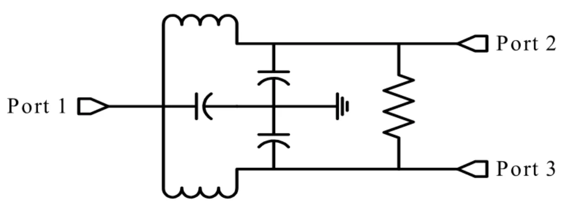
Because resistive attenuator in the feedback loop will degrade of white phase noise floor, an unequal Wilkinson power splitter is employed to adjust the excess small signal loop gain instead of resistive attenuator. [33] The Wilkinson power splitter can be realized as lump component or transmission line designs. To save the volume, the circuit is realized by the lump reactive components instead of microstrip line as shown in Fig. 2-7.
Port 3
Port 1
Port 2
2.2.5 Electronic Phase Shifter
The electronic phase shifter is used to tune electronically the oscillation frequency. The electronic phase shifter is constructed with silicon tuning diodes and inductors using T-circuit as shown in Fig. 2-8. It is basically a tunable high pass filter which, except for providing variable phase shifter in the loop, suppresses the excess gain of the loop amplifier at low frequency, preventing it from spurious oscillation. The phase noise and tuning linearity will be affected by the tuning diodes. High residual phase noise of tuning diodes will degrade the phase noise of voltage-controlled oscillator. With proper selection of varactor diodes, the high tuning linearity and low phase noise are achieved at the same time.
Fig. 2-8 Electronic phase shifter.
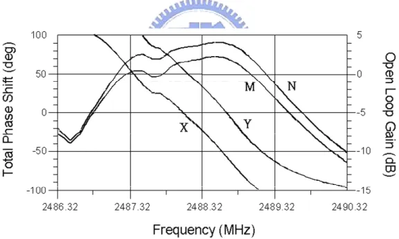
The phase shift of loop amplifier and power splitter is about equal to -80° and 90°, respectively. The electronic phase shifter is about 40°. Because the total phase shift around the loop must be 2πN radians, another 10° is required, which is from the loop phase adjust constructed with fixed lumped reactive components. The frequency dependences of total phase shifter and open loop gain seen from the reference plane
A-B line indicated in the Fig. 2-5 are shown in Fig. 2-9. Curve X and Curve Y are the total phase shift with Vtune = 0Volts and Vtune = 5Volts, respectively. Curve M and
curve N are the respective open loop gain with Vtune = 0Volts and 5Volts, respectively.
The group delay is about 1.74×10⁻⁶rad/Hz. As compared to Fig. 2-6(d), we see that the SAW resonator dominates the phase shift. The slight increase in group delay may be from the tunable phase shifter with varactors. The oscillation frequency is predicted at the zero-crossing point with enough gain margins about 2dB. This gives us the benefit of low flicker noise from the amplifier without deep gain compression. The tuning bandwidth is approximately equal to the resonator’s 1dB bandwidth. It is approximately from 2487.85 MHz to 2488.85 MHz. The tuning bandwidth is approximately equal to the resonator’s 1dB bandwidth.
Fig. 2-9 Total phase shifter and the open loop gain at the oscillation frequency.
2.2.6 Oscillator Performance
The performances of the oscillator with STW resonator are measured. The narrow and wide scan of output spectrum and relative levels of harmonic are shown in Fig. 2-10(a) and (b), respectively. Because the STW resonator do not have 2nd harmonic response and the bandwidth of the loop amplifier is limited at 4 GHz, the
2nd harmonics of oscillator is suppressed below 58 dB as shown in Fig. 2-10(b) without any output low pass filter. The tuning characteristic is shown in Fig. 2-11 with ±200ppm range and good linearity. The frequency dependence on temperature is illustrated in Fig. 2-12. The turnover temperature is approximately 45°C, which is mainly determined by the SAW resonator.
(a)
(b)
Fig. 2-10 (a) Measured output spectrum for the 2488.32 MHz and (b) harmonics spectrum.
Fig. 2-12 Dependence of the oscillation frequency on temperature.
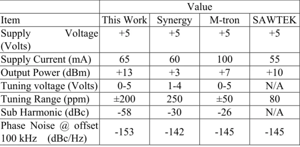
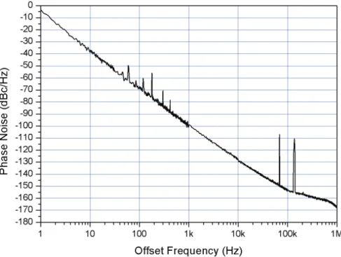
The phase noise of the oscillator is measured as shown in Fig. 2-13. The measured parameters of the STW oscillator and the specifications of the other commercial products are summarized in Table 2.1.
Table 2.1: Measured results for the voltage-controlled STW oscillator and comparison with the other commercial products.
Value
Item This Work Synergy M-tron SAWTEK
Supply Voltage (Volts)
+5 +5 +5 +5
Supply Current (mA) 65 60 100 55
Output Power (dBm) +13 +3 +7 +10
Tuning voltage (Volts) 0-5 1-4 0-5 N/A
Tuning Range (ppm) ±200 250 ±50 80
Sub Harmonic (dBc) -58 -30 -26 N/A
Phase Noise @ offset
2.3 Voltage Controlled Oscillator with FBAR
After the success development of 2488 MHz voltage-controlled oscillator with STW resonator, we try to use the FBAR to replace the STW resonator. Basically, the suspended FBAR device is a three-layer structure with the top and bottom electrodes sandwiching a middle layer of oriented piezoelectric material. Air interfaces are used on both outer surfaces to prevent acoustic energy leaking out of the device; as the solid membrane and air boundary form high impedance to acoustic wave, functioning as high-Q acoustic reflectors at all frequency. When RF signals are applied near the mechanical resonant frequency, the piezoelectric transducer excites the fundamental bulk compress wave traveling perpendicular to the films. Resonators for use in stable oscillators need low temperature coefficient (TC), which needs composite structures for positive and negative coefficient compensation. On the contrary, for temperature sensing, a higher degree of TC is required for sensitivity, which is achieved also though composite structure containing all positive (or negative) coefficient material.
Here, AlN is employed for the potential integration. AlN has a crystal structure of hexagonal wurtzite where aluminum and nitrogen atoms are combined. AlN film is grown along (002) direction to achieve high piezoelectric coupling to the required extensional mode. AlN lattice extends and retracts toward c-axis orientation creating vibration if an alternating field is applied cross the crystal.
In this section, a high quality factor FBAR was designed and fabricated. Using this resonator, a high frequency voltage-controlled FBAR oscillator is designed and realized with hybrid circuits.
2.3.1 FBAR Design and Fabrication
It was reported that the lower the full width at half maximum (FWHM) value of a piezoelectric material has, the better the performance characteristics of the resonators and filters has. [34] Thus, the AlN piezoelectric film needs to have highly c-axis oriented columnar structure. [35] To achieve this requirement, a SiNX thin film
is added between AlN and bottom electron. [36] The SiNX layer also serves as an
etching stop layer to protect bottom electron while patterning the AlN layer.
The resonant frequency of FBAR is predominantly determined by half wavelength of standing acoustic wave in the resonator. The fundamental resonant frequency is then inversely proportional to the thickness (d) of the piezoelectric material used, and is equal to Va /2d, where Vais an acoustic velocity at the resonant
frequency. The Nth harmonic frequency of the FBAR can be approximated as
) ( 2 _ _ _ _ b elec b elec SiN SiN piezo piezo t elec t elec r V d V d V d V d N f + + + ≈ , (2.4)
where delec_t, dpiezo, dSiN, and delec_b are the thickness of top electrode (Al), piezoelectric
material (AlN), buffer layer (SiNX), and bottom electrodes (Cr/Au), respectively.
Velec_t, Vpiezo, VSiN, Velec_b are the acoustic velocities of top electrode (Al), piezoelectric
material (AlN), buffer layer (SiNX), and bottom electrodes (Cr/Au) respectively.
According to equation (2.4), the thickness of each layer in the FBAR for fundamental frequency (N=1) at 2.48 GHz for unlicensed application was designed and listed in Table 2.2.
Table 2.2: Physical properties of representative materials for FBAR. [37-39]
Layer Metal Piezoelectric Buffer Metal
Layer material Al AlN SiNX Cr/Au
Density (kg/m3) 2700 3255 3270 19700
Acoustic velocity (m/s) 6420 10400 11000 3240 (Au)
Designed thickness (Å) 3500 11000 1000 1000
Thermal expansion
coefficient (ppm/oC) 23.6 4.6 0.8 14.4
It is well known that AlN films must be grown orientated in the (002) direction to achieve high piezoelectric coupling to the required extensional mode. Therefore columnar AlN grains whose c-axes are perpendicular to the substrate are needed. The four layered composite structure Al/AlN/SiNX/Au of FBAR is shown in Fig. 2-14.
AlN was fabricated on (100) crystallographic oriented epitaxial silicon wafers. After RCA cleaning, silicon wafer was deposited with low stress silicon nitride (Si3N4)
using Low Pressure Chemical Vapor Deposition (LPCVD) and the thickness is 1200Å. The Si3N4 layer served both as a high resistivity substrate to eliminate any parasitic
contributions from mobile charges or a highly boron-doped epitaxial layer and an etch obstruction layer. Temporary support (sacrificial layer: Cu) is formed by E-gun on top of Si3N4 followed by electrode and piezoelectric layer. Then, a thin layer of Cr/Au
film which thickness is 1000Å was fabricated by electron beam evaporation and patterned using lift-off process and serves as the bottom electrode. The AlN film deposited on bottom electrode has poor c-axis crystallinity. To overcome this weakness of bottom electrode, SiNX buffer layer is introduced prior to the deposition
of bottom electrode. An amorphous SiNX film which thickness is 1000Å was
fabricated by Plasma Enhanced Chemical Vapor Deposition (PECVD) and served as a buffer layer between bottom electrode and piezoelectric layer. [40] An AlN film was then fabricated on top of the buffer layer through pulsed reactor DC magnetron sputtering and the substrate temperature (300oC) was kept. The thickness of AlN is about 11000Å. The fourth layer of an aluminum film which thickness is 3500Å was fabricated by electron beam evaporation and patterned by photolithography as a top electrode. The active area of FBAR is only about 70 x 70um to reduce the parasitic capacitance from electrodes for the purpose of high frequency operation. The copper temporary support which thickness is 5000Å was removed by wet etching using ASP100 and leaving a membrane resonator supported at the edges. The die photo is shown in Fig. 2-15.
Fig. 2-15 Picture for the Film Bulk Acoustic Resonator
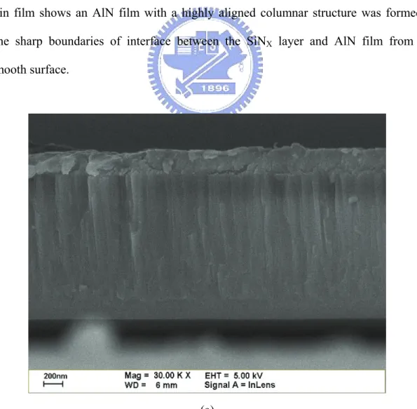
Fig. 2-16(a) and (b) show the cross-sectional SEM photograph of (002)-oriented AlN film, lie on SiNX buffer layer and bottom electron. The cross section view of the
thin film shows an AlN film with a highly aligned columnar structure was formed. The sharp boundaries of interface between the SiNX layer and AlN film from a
smooth surface.
(b)
Fig. 2-16 Cross-sectional SEM photograph of (002)-oriented AlN film with SiNX
buffer layer (a) 30000X, (b) 60000X.
The FBAR sensors were probed at wafer level to measure the resonant behavior. The Agilent 8510C Vector Network Analyzer, controlled automatically by program, was employed to acquire the S-parameters. Fig. 2-17 shows the Z-parameter impedance characteristics calculated from the measured S-parameters. The resonator reveals two resonant frequencies characterized by a zero phase shift. One is a series resonance frequency (denoted by fS) with minimum impedance and zero phase shift,
which occurs as piezoelectric coupling is in phase with an applied voltage. The other is a parallel resonance frequency (denoted by fP) with maximum impedance and zero
phase shift, which occurs as piezoelectric coupling is 180 degrees out of phase with an applied voltage.
2.35 2.45 2.55 2.65 2.25 2.75 -45 0 45 -90 90 10 20 30 40 0 50 Frequency (GHz) M agnit ude ( Z ) P hase ( Z )
Fig. 2-17 Z-parameters of the FBAR.
2.3.2 Oscillator Design
With the success of FBAR, an oscillator was designed and fabricated. Its functional block is illustrated in Fig. 2-18. The architecture with FBAR forms a feedback loop. It consists of a single loop amplifier, a Wilkinson power splitter, a phase adjusting, and a FBAR resonator. The HBT monolithic amplifier is selected as the loop amplifier because of low noise figure and high dynamic range. The P1dB is at +17dBm and the bandwidth is 4 GHz. Its bandwidth was properly selected to prevent high 2nd harmonics. The nominal gain of 17dB is much greater than that required to overcome the total loop losses to insure the stable oscillation. The magnitude of gain variation over temperature is approximately 0.005dB/oC and this feature can prevent the temperature variation of oscillator. The power divider and phase shift were made of lumped elements. The resonator acts as a short circuit with zero phase-shift at the desired frequency. The oscillation occurs as the closed loop gain satisfies Barkhausen criteria.[41] During design phase, the open loop gain (S21) is
actually evaluated by breaking the loop at the appropriate plane with equal input and output impedance, such as line AB noted in Fig. 2-18. The linear simulation is performed by using Agilent Advance Design System (ADS) software and shown in Fig. 2-19. The oscillation starts when the phase of S21 equal to zero and |S21| > 1,
which in turn implies the equivalent resistance is negative. The Barkhausen criteria are satisfied simultaneously.
Fig. 2-18 Block diagram of a feedback loop oscillator.
2.465 2.470 2.475 2.480 2.485 2.490 2.495 2.460 2.500 -20 0 20 40 60 -40 80 -10 -5 0 -15 5 Frequency (GHz) |S 21 | (dB ) ∠ S21 (degree)
2.3.3 Measurement and Discussion
The fundamental and higher harmonics oscillation spectrums were measured and shown in Fig. 2-20 (a) and (b), respectively. The 2nd harmonics of oscillator is suppressed below 40 dB as shown in Fig. 2-20(b). The oscillation frequency is slightly higher than the series resonance frequency fS of FBAR because of the
parasitic capacitance from package effect. The variation of fundamental frequency with temperature was also measured and shown in Fig. 2-21. The TC of oscillator is about -34.5ppm/oC and seems to be equal to that of FBAR. It implies that the effective tank of the oscillator is dominated by the FBAR resonator. The tuning characteristic is shown in Fig. 2-22 with ±6% range. The performances of the oscillator with FBAR resonator are measured and summarized in Table 2.3.
Table 2.3: Measured Results for the FBAR oscillator.
Item Value Supply Voltage (Volts) +5.0
Supply Current (mA) 65
Output Power (dBm) +14.5
Tuning Voltage (Volts) 0-5
Tuning Range > ±6%
(a)
(b)
Fig. 2-20 (a) Output fundamental spectrum, and (b)harmonics spectrum for the oscillator.
10 20 30 40 50 60 70 80 2430 2440 2450 2460 2470 2480 2490 2500 2510 F req uency (MHz) Temperature(°C) fp(FBAR) Oscillator fs(FBAR)
Fig. 2-21 Measured variation of fundamental frequency with temperature for FBAR and oscillator.
Chapter 3
Measurement and Prediction of Phase Noise in
Oscillator with STW Resonator
3.1 Introduction
Frequency stability can be defined as the degree to which an oscillating source produces the same frequency throughout a specified period of time. Every RF and microwave source exhibits some amount of frequency instability. This stability can be broken down into two components: one is long-term stability, the other is short-term stability. Long-term stability describes the frequency variations that occur over long time periods, expressed in parts per million per hour, day, month, or year. Short-term stability contains all elements causing frequency changes about the nominal frequency of less than a few seconds duration. Here, we just focus on the short-term stability.
Phase noise is the important specification for an oscillator. The absolute phase noise of an oscillator is set by the residual noise of the active devices, the residual noise of the resonator and the bandwidth of the resonator. Generally the active devices in the oscillator are the major noise contributors. In the design phase, we found that the active devices with lower noise figure could not always lead to the oscillator with lower phase noise. After examining the residual phase noise of the major components in the oscillator, we found the residual phase noise of the STW resonator dominates the phase noise of the oscillator instead of the active devices and the lower noise figure of active devices do not relate to the lower residual phase noise.
Here, the Agilent’s E5503B phase noise measurement system is used for residual phase noise and absolute phase noise measurements. A phase noise prediction method based on residual phase noise of devices in oscillators is presented in this chapter.
3.2 Residual Phase Noise of Devices
3.2.1 Residual Noise
Residual noise (or two-port noise) is the noise added to signal when the signal is processed by a two-port device. Such devices include: amplifiers, dividers, filters, mixers, multipliers, phase-lock loop synthesizers, or any other two-port electronic networks. Residual noise contains both AM and PM components. [42-44]
There are two basic noise mechanisms in residual noise: one is additive noise, the other is multiplicative noise. Residual noise is the sum of additive and multiplicative noise. Additive noise, as shown in Fig. 3-1, is generated by the two-port device at or near the signal frequency and added in a linear fashion to the signal. Multiplicative noise has two known causes. One is an intrinsic, direct phase modulation with 1/f spectral density and the exact origin of this noise component is unknown. The other is noise may modulate an RF signal by multiplying baseband noise with the signal, as shown in Fig. 3-2. This mixing is due to any non-linearities in the two-port network. The baseband noise may be produced by the active devices active devices of the internal network, or may come from low-frequency noise on the signal or power supply.
Fig. 3-1 Additive noise component.
3.2.2 Measurement Process of Residual Phase Noise
The basic residual phase noise measurement setup is shown as Fig. 3-3. An unmodulated signal source with low AM noise is necessary. The AM noise of the source which used for residual phase noise measurement must be comparatively small because the mixer type phase detector has only 20 to 30 dB of AM noise rejection. If the AM component of the source is greater than 20 to 30 dB above the residual phase noise of the device-under-test (DUT), it will contribute to the residual phase noise measurement and show the residual phase noise as being greater than it really is. The noise floor of measurement system is established by replacing the DUT with a feed-through and adjusting the total insertion loss in the device test path to maintain the proper RF signal power level to the R-port (LO-port) of the phase detector. Phase quadrature for two input ports of the phase noise detector is established by using a mechanical line stretcher. The electronic phase shifter is not proper because of its high residual noise. A critical point is to maintain the constant RF power level to the L-port (device test path) and R-port for the phase detector during calibration as well as during the actual measurement. The source noise in each of the two phase detector paths is correlated at the phase detector for frequency offset range of interest. When the source noise is correlated at the phase detector, the source phase noise cancels, leaving only the residual phase noise of the DUT. Agilent E5503B noise measurement system is used for the residual phase noise measurement. Fig. 3-4 shows the E5503B connection diagram for residual phase noise measurement and the system noise floor is shown in Fig. 3-5. The spurious signals which closed to the carrier are the system spurious, primary 60 Hz (and harmonics) power line spurs.
A bandpass filter type response will cause the source noise to be decorrelated at the edge of the filter. This decorrelation of noise causes the system to measure the source noise level directly at the offsets beyond the filter bandwidth.
Fig. 3-3 The basic setup for residual phase noise measurement.
Fig. 3-5 Measured noise floor for residual phase noise measurement system.
3.2.3 Residual Phase Noise of Main Components in Oscillator
There are three major noise contributors in this feedback loop oscillator: STW resonator, loop amplifier and electronic phase shifter.
Residual phase noise in a SAW or STW resonator occurs when an unmodulated carrier is passed through the acoustic device. In this process, phase fluctuations which occur in the resonator cause a direct phase modulation of the carrier so that it appears with PM modulation noise sideband at the device output.[43] The residual phase noise of the STW resonator is shown in Fig. 3-6. It is measured by applying the power approximately the same power level in the steady state oscillation condition. The corner of the flick noise is out of the scope of this measurement.
Fig. 3-6 Residual phase noise of STW resonator.
The residual phase noise of the loop amplifier is shown in Fig. 3-7. The noise floor is approximately -170dBc/Hz with a 1/f flicker noise corner at 17 kHz. Noise figure is the ratio of the output noise of an amplifier referred back to the input divided by the thermal noise floor. Noise figure is a common specification that is used to calculate the noise at Fourier frequencies f that are far from the carrier frequency. The noise figures listed in the data sheets of actives devices are small signal noise figures, not dynamic noise figure. The dynamic noise figures are measured under actual large signal conditions and may differ from the small signal noise figures. It includes the multiplicative noise produced by the non-linearities of active device, in the presence of a large signal. In the presence of a carrier signal, the noise level is no longer
constant but often increases as f decreases. This increase usually changes at a rate of at least 1/f, “flicker” behavior, which often significantly dominates over the white-noise level given by the NF, which in practice is measured in the absence of an actual signal through the amplifier. Furthermore, the flicker- noise level depends on the amplifier’s linearity and input power. Because of this signal induced rise in amplifier noise, many systems do not achieve the performance predicted by using the no-signal NF characterization. The dynamic noise figure can be expressed as:[45]
in TH P N f − + =L( ) NFD
Where NFD is the dynamic noise figure in dB, NTH is the thermal noise, Pin is the
input signal power in dBm, and the L(f) is the residual phase noise in dBc/Hz.
The electronic phase shifter is mainly constructed varactors and inductor. The varactors are the noise contributors. The residual phase noise performance for the electronic phase shifter is measured and shown in Fig. 3-8.
Fig. 3-8 Residual phase noise of electronic phase shifter.
3.3 Absolute Phase Noise of Oscillators
The phase noise test characterizes the output spectral purity of an oscillator by determining the ratio of desired energy being delivered by the oscillator at the specified output frequency to the amount of undesired energy being delivered at neighboring frequencies. This ratio is usually expressed as a series of power measurements performed at various offset frequencies from the carrier. The power measurements are normalized to a 1 Hz bandwidth basis and expressed with respect to
the carrier power level.
3.3.1 Phase techniques of absolute phase noise measurements
There are three dominant techniques used to measure the phase noise of oscillators: the direct spectrum analyzer approach, the phase-lock-loop (PLL) techniques, and the discriminator techniques.[46] The most direct and probably the oldest method used to measure the phase noise of oscillators is the direct spectrum analyzer method. Here the signal from the device-under-test (DUT) is input to a spectrum analyzer tuned to the DUT frequency. The sideband noise power can be directly measured and compared to the carrier signal power to obtain the phase noise spectrum. This method actually measures the total sideband noise, including AM noise and phase noise. If AM noise is much less than the phase noise, the measurement can be considered as to be the phase noise. The sensitivity of this method is limited by the internal local oscillator (LO) noise of the spectrum analyzer, and the inability to track any signal drift limits the close-to-carrier noise measurement capability of the analyzer.
When the AM noise is relatively high to the phase noise, a phase detector is required to separate the phase noise from the amplitude noise. The phase detector converts the phase difference of the two incident signal in to a voltage at the output of the detector. When the phase difference between the two input ports of the detector is set to 90 degree, the voltage output will be zero volts. Any phase fluctuation from quadrature will result in a voltage fluctuation at the output. When the quadrature is not maintained, an error can be introduced into results based on the amount of the phase delta from quadrature. The error is 20 log [cos (phase deviation from quadrature)] (dB). Phase detectors are usually constructed by the double balanced mixers, and typically required large power signals at the input port to operate properly.
One of the signals must be of high power to switch the diodes in the detector, allowing the other signal to be of lower power.
There are two different measurement techniques which use a phase detector, along with associated filters, low noise amplifier, and baseband analyzer: one is the PLL with reference source measurement technique, and the other is FM discriminator measurement technique. Within the PLL with reference source measurement technique, another source is used to provide the reference phase signal for the phase detector. This is the standard measure of phase fluctuations described in NIST Technical Note 1337. Fig. 3-9 shows a block diagram of the method suggested by NIST.
Fig. 3-9 General block diagram described in NIST technical note 1337.
Signals from two oscillators at the same nominal frequency are applied to the mixer inputs. The PLL is used to controlled either of the two sources and establish phase quadrature at the input ports of the phase detector. This means that one of the two sources used in this method must have DC voltage control capability for phase
locking. A very narrow band PLL is used to maintain a 90 degree phase difference between these two sources. The phase detector operation is such that when the input signals are 90 degrees out of phase (in quadrature), the output of the mixer is a small fluctuating voltage proportional to the phase difference between the two oscillators. By examining the spectrum of this error signal on the spectrum analyzer, the phase noise performance of this pair of oscillators may be measured. If the noise of one oscillator dominates, its phase noise is measured directly. A useful and practical approximation when the two test oscillators are electrically similar is that each oscillator contributes one-half the measured noise power. When three or more oscillators are available for test, the phase noise of each oscillator may be accurately calculated by solving simultaneous equations expressing data measured from the permutations of oscillator pairs. The frequency difference between the two sourced at the phase detector must be less than 10% of the peak-tuning-range (PTR) for PLL to close. High PTR will cause the increase in the system noise floor. This feature makes this technique is not suitable for measuring the high-drift-rate low phase noise sources which requires high PTR. Lower power from the DUT or the reference source can cause the phase detector noise floor to rise or the phase detector to not operate. Low noise amplifier prior to the phase detector can help to solve this problem, but the residual noise of the amplifiers will add to the phase detector phase noise floor. The increase in the system noise floor will degrade the sensitivity of the phase detector. The residual noise of the amplifier becomes a limiting factor in the overall system measurement noise floor.
The oscillators with SAW or STW resonators have both low phase noise and high drift rate characteristics. So, the direct spectrum techniques and the PLL with reference source measurement techniques are not fulfilling the requirement while measuring the low phase noise oscillator with piezoelectric resonator. FM
discriminator technique is the hopeful candidate for measuring these low phase noise SAW oscillator. The theory and design consideration are describe as follows.
3.3.2 Theory of FM discriminator [46,47]
The basic block diagram for frequency discriminator is shown as Fig. 3-10. Unlike the PLL phase detector method, the frequency discriminator method does not require a second reference source phase locked to the source under test. This makes the frequency discriminator method extremely useful for measuring sources those are difficult to phase lock, including sources those are microphonic or drift quickly. It can also be used to measure sources with high-level, low-rate phase noise, or high close-in spurious sidebands, conditions with can pose serious problems for the phase detector method. A wide-band delay line discriminator can be implemented using a low loss coaxial cable. A resonator can also be applied for the narrow-band delay line discriminator. Delay line discriminators are only capable of measuring phase type random noise and are in fact insensitive to AM noise. Typically AM rejection for the delay line discriminator is greater than 20dB.
![Table 2.2: Physical properties of representative materials for FBAR. [37-39]](https://thumb-ap.123doks.com/thumbv2/9libinfo/8762502.208511/40.892.128.772.147.445/table-physical-properties-representative-materials-fbar.webp)