國 立 交 通 大 學
電子工程學系電子研究所
碩 士 論 文
以濺鍍法製備之鋯酸鍶記憶體元件具有無電壓極性
之電阻轉換特性研究
Nonpolar Resistive Switching Properties of
Sputter-Deposited SrZrO
3Memory Devices
研 究 生:尤俊勝
指導教授:曾俊元
以濺鍍法製備之鋯酸鍶記憶體元件具有無電壓極性之電阻轉換特
性研究
Nonpolar Resistive Switching Properties of Sputter-Deposited SrZrO
3Memory Devices
研 究 生:尤俊勝
Student:
Jung-Sheng
Yu
指導教授:曾俊元
Advisor:
Tseung-Yuen
Tseng
國立交通大學 電子工程學系電子研究所
碩 士 論 文
A Thesis
Submitted to Department of Electronics Engineering and Institute of Electronics
College of Electrical and Computer Engineering National Chiao Tung University
in partial Fulfillment of the Requirements for the Degree of
Master
in Electronics Engineering
July 2007
Hsinchu, Taiwan, Republic of China
以濺鍍法製備之鋯酸鍶記憶體元件具有無電壓極性之電阻轉換特
性研究
研究生:尤俊勝 指導教授:曾俊元
國立交通大學
電子工程學系電子研究所
摘要
近來由各種材料所研製的各種新世代非揮發性記憶元件受到廣泛的注意,其中又以 電阻式記憶元件最受囑目,由於其具有雙穩態導電性,可在同一偏壓下表現出兩種不同 導電率之特性,並且具有高寫入及讀取速度、非破壞性讀取及結構簡單的優點,將有助 於達到高密度積體整合及低操作功率的目的,因此電阻式記憶體儼然成為下一世代非揮 發性記憶體之候選人。 本論文利用鈣鈦礦結構材料(鋯酸鍶)作為電阻式記憶體的材料,首先本論文將介 紹新世代非揮發性記憶體之應用、特性以及優點,本論文中也將探討各種可能的電阻轉 換機制及傳導機制。在實驗的部分,我們利用射頻磁控濺鍍法製備釩摻雜的鋯酸鍶薄膜 作為轉換電阻層,且利用此濺鍍法沉積鎳酸鑭作為幫助鋯酸鍶成長優選方向之緩衝層, 底電極白金及頂電極鋁則利用蒸鍍法製備,形成一頂電極/電阻層/緩衝層/底電極的結 構,其物理及電學特性我們將於第四章深入探討之,此外我們也將探討元件的記憶體特 性,並比較及探討不同元件結構對記憶體特性的影響,更進一步由實驗結果來探討可能 的電阻式記憶體的電阻轉換及傳導機制。Nonpolar Resistive Switching Properties of Sputter-Deposited SrZrO
3Memory
Devices
Student: Jung-Sheng Yu
Advisor: Tseung-Yuen Tseng
Department of Electronics Engineering and Institute of Electronics
National Chiao Tung University
Abstract
Recently, many kinds of next-generation nonvolatile memories, such as resistive random access memory (RRAM) and phase change memory, have attracted a lot of attention. Because of the RRAM possesses the bistable conductivity switching characteristics, the device can exhibit two different conductivities at the same applied voltage. In addition, the RRAM with high operation speed, nondestructive readout, and simple device structure are helpful for high density of integration and lower power consumption. Therefore, the RRAM has been proposed to be a possible candidate of next-generation nonvolatile memories.
In this thesis, the RRAM devices manufactured based on SrZrO3 (SZO) thin films are
studied and developed. At first, I will introduce the applications, fundamental characteristics, and advantages of next-generation nonvolatile memories. The conduction mechanisms of RRAM that have been published are also discussed. In experimental details, V2O5 doped SZO
film was deposited on the LaNiO3 buffer layer by RF magnetron sputter. Pt and Al act as
bottom electrode and top electrode, respectively. Therefore, electrode/resistive thin film/buffer layer/electrode structure is formed. The physical and electrical properties of the device are reported in chapter 4. Besides, the memory effects of the device are also presented, which nearly matches the criteria of RRAM. The resistive switching polarity is also compared the difference with various device structures. Furthermore, the possible resistive switching mechanism based on the research results is also discussed in this thesis.
誌謝
首先,要感謝我的指導教授曾俊元教授在我兩年的研究生生涯裡,提供這麼豐富的 研究資源,並在專業領域上給予我許多的指導,讓我成長了許多。有幸能跟著老師學習, 是我就讀研究所最大的收獲之一。 此外,也要感謝國家毫微米實驗室、清大貴重儀器中心、交大貴重儀器中心等單位, 提供良好的研究環境,在此也一併致謝! 還要謝謝林群傑學長、林志洋學長,在我實驗、課業以及論文上總是給予我很多的 指教,並能隨時指出我的錯誤,讓我能夠在這兩年安然地度過,實在很感激他們。還要 一併感謝林昭正學長、林孟漢學長、王勝裕學長在實驗上也給予我很大的協助。還有吳 鎮宇、陳冠仲、黃俊興、吳重毅、余松蒔、姚承佑、簡士傑這幾位同學,很感謝有你們 的陪伴,使得我生活中增添了許多歡樂,很感激這兩年有你們的陪伴,曾經一起去過的 地方,聊過的話題,都是我最珍貴的回憶,我會好好珍惜這一份難得的友誼。黃毅函、 詹世偉、翁啟翔、顏宏全、莊文仁這幾位學弟,多謝你們在實驗上的幫忙。還有曾給予 我協助的朋友,若沒有你們,我也不會這麼順利。 最後還要感謝我的家人,很感謝你們這麼的支持我讀研究所,在你們的支持下,讓 我無後顧之憂能順利完成研究所學業。可惜的是,在我畢業前一個月,我最親愛的奶奶 過世,很遺憾她無法看到我畢業,我想把這份論文獻給她,跟她說我好想她,希望她在 天上能夠很快樂。Contents
Chinese Abstract ………. i
English Abstract ……….. ii
Acknowledgement……….………….. iii
Contents ………... iv
Table Captions ………. viii
Figure Captions ………... ix
Chapter 1 Introduction 1 1.1 Introduction to Memories ………. 1
1.1.1 Volatile Memory ……….... 1
1.1.2 Nonvolatile Memory ………. 1
1.2 Introduction to Nonvolatile Memory ………...… 2
1.2.1 Read Only Memory ………... 3
1.2.2 Programmable Read Only Memory ………...……... 3
1.2.3 Erasable and Programmable Read Only Memory ………. 3
1.2.4 Electrically Erasable and Programmable Read Only Memory ………. 4
1.2.5 Flash ……….. 4
1.3 Next-Generation Nonvolatile Memories ……….. 4
1.3.1 Semiconductor-Oxide-Nitride-Oxide Semiconductor ………... 5
1.3.2 Ferroelectric Random Access Memory ………. 6
1.3.3 Magnetoresistive Random Access Memory ……….. 7
1.3.4 Phase Change Random Access Memory ………... 8
1.3.5 Resistive Random Access Memory ……….. 9
Chapter 2 Experiment Details 18
2.1 Experiment Process Flow ………. 18
2.2 RF Magnetron Sputter Systems………. 19
2.2.1 Vacuum System ………. 19
2.2.2 Pressure System ………. 19
2.2.3 Temperature Controlling System ………... 20
2.2.4 Gas Flow Controlling System ………... 20
2.2.5 Plasma Controlling System ………... 20
2.2.6 Cooling System ………. 21
2.3 Preparation of Devices ………. 21
2.3.1 Preparation of Sputter Targets ………... 21
2.3.2 Thin Film Depositions ………... 22
2.3.3 Heat Treatment after Thin Film Depositions ………. 23
2.3.4 Deposition of Top Electrode ……….. 23
2.4 Measurements and Analyses ……… 24
2.4.1 X-Ray Diffraction ………. 24
2.4.2 Scanning Electron Microscope ……….. 25
2.4.3 Focus Ion Beam ……….… 25
2.4.4 Field Emission Transmission Electron Microscope and Energy Dispersive X-Ray Spectrometer ………. 26
2.4.5 Scanning Probe Microscope ……….. 26
Chapter 3 Possible Mechanisms of Conductivity switching Phenomenon 34
3.1 Conductance Filament ……….. 35
3.2 Charge Transfer ……… 36
3.3 Storage and Release of Charge Carriers ………... 37
3.4 Dipole Rearrangement Induced Polarization ………... 38
3.5 Phase Transformation ……….. 38
3.6 Formation of the Depletion Layer ……… 39
Chapter 4 Results and Discussion 41 4.1 Properties and Analyses of the LaNiO3 Buffer Layer and SrZrO3 Resistive Films ………. 41
4.1.1 X-Ray Diffraction and Scanning Electron Microscope Analyses of the LaNiO3 Buffer Layer ……… 41
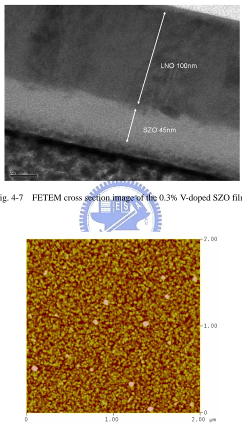
4.1.2 Transmission Electron Microscope ………... 43
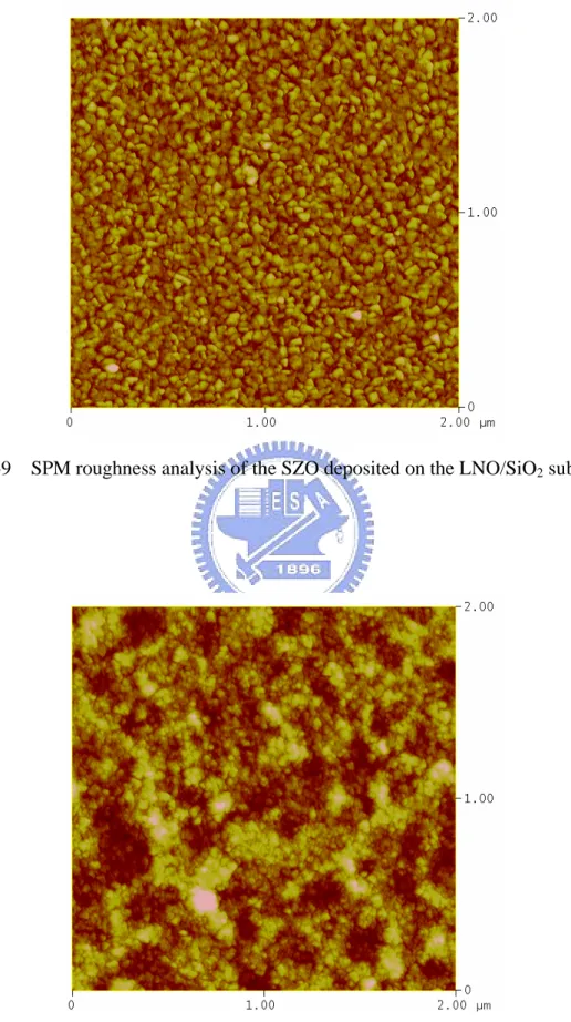
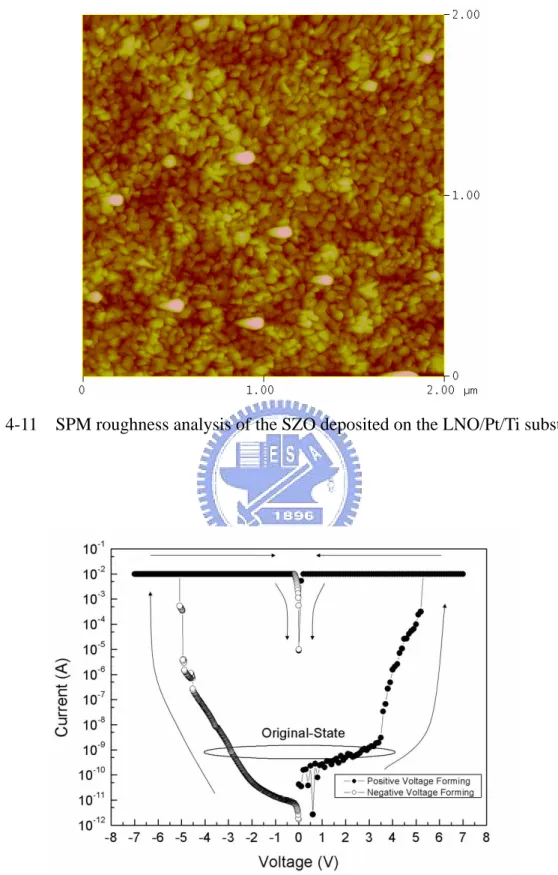
4.1.3 Scanning Probe Microscope ……….. 44
4.2 Electrical and Physical Properties of the Al/V-doped SrZrO3/LaNiO3/Pt ...……. 44
4.2.1 Forming Process ……… 44
4.2.2 SrZrO3 Sputtering Parameters ……….. 45
4.2.3 Electrical Properties of SrZrO3 Resistive Films ……… 45
4.2.4 Schematic Conducting Loop ………. 46
4.2.5 Conducting Mechanisms ………... 47
4.2.6 Possible Resistive Switching Mechanisms ………... 48
4.3 Test of Memory Effects ……… 48
4.3.1 Retention ………... 49
4.3.3 Non-Destructive Readout ……….. 50 4.3.4 Thermal Reliability ………... 50 4.3.5 Endurance ………. 50 4.4 Different Electrode Material Affecting Resistive Switching Properties of the
Device ………... 51
4.5 One Diode and One Resistor Device ……… 53
Chapter 5 Conclusions 75
Table Captions
Chapter 3
Table 3-1 Basic conduction mechanisms in insulators [27].
Chapter 4
Table 4-1 Conductivities of the LNO films with different sputtering temperature and annealing ambience.
Table 4-2 Roughness of the SZO and LNO films deposited on different substrates.
Table 4-3 Resistive switching properties of the SZO-, TiO2-, and PCMO-based
devices [15], [41]-[46].
Chapter 5
Figure Captions
Chapter 1
Fig. 1-1 Typical floating gate memory structure. Fig. 1-2 Cross-section image of the SONOS structure. Fig. 1-3 ABO3 perovskite unit cell [3].
Fig. 1-4 Hysteresis loop of the ferroelectric material [3]. Fig. 1-5 Fundamental concept of the phase change materials.
Fig. 1-6 Schematic plot of a PCRAM cell. Depending on the state of the active region (crystalline or amorphous) the resistance of the cell changes by several orders of magnitude.
Fig. 1-7 I-V curve of a PCRAM cell. SET and RESET denote the switching regions, while READ denotes the region of readout.
Fig. 1-8 Cross section schematic diagram of the RRAM. The transistor is fabricated in the front and the resistor in the back end [16].
Fig. 1-9 Equivalent circuit of an array for the write operation of a given bit resistor [17].
Fig. 1-10 Describing how leakage current paths make cell resistance misread [24].
Chapter 2
Fig. 2-1 Illustration of the experimental flow. Fig. 2-2 Preparation flow of the device.
Fig. 2-3 Cross section of the four-layer structure device. Fig. 2-4 Cross section of the tri-layer structure device.
Fig. 2-5 Illustration of the sputter system. Fig. 2-6 Synthesis flow chart of LNO powder. Fig. 2-7 Synthesis flow chart of doped SZO powder.
Chapter 4
Fig. 4-1 XRD patterns of the LNO buffer layer with different substrates. Fig. 4-2 SEM surface micro-morphology of the as-deposited LNO buffer
layer.
Fig. 4-3 XRD patterns of the LNO buffer layer with different RTA temperatures.
Fig. 4-4 SEM surface morphology of the LNO after 600oC RTA treatment. Fig. 4-5 SEM surface morphology of the LNO after 700oC RTA treatment. Fig. 4-6 SEM surface micro-morphology of the 0.3% V-doped SZO film. Fig. 4-7 FETEM cross section image of the 0.3% V-doped SZO film.
Fig. 4-8 SPM roughness analysis of the LNO deposited on the SiO2 substrate.
Fig. 4-9 SPM roughness analysis of the SZO deposited on the LNO/SiO2
substrate.
Fig. 4-10 SPM roughness analysis of the LNO deposited on the Pt/Ti electrode. Fig. 4-11 SPM roughness analysis of the SZO deposited on the LNO/Pt/Ti
substrate.
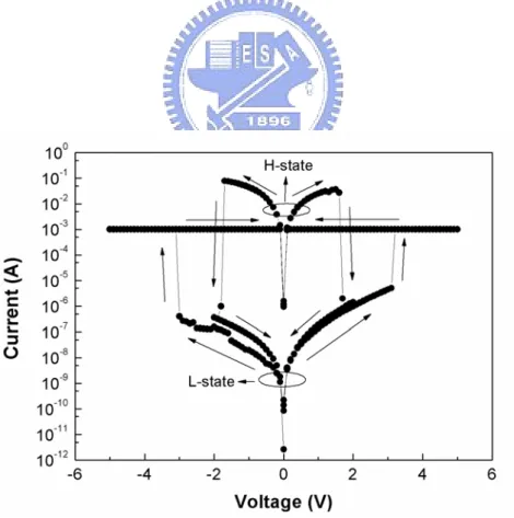
Fig. 4-12 I-V curve of the Al/0.3% V-doped SZO/LNO/Pt device with forming voltage.
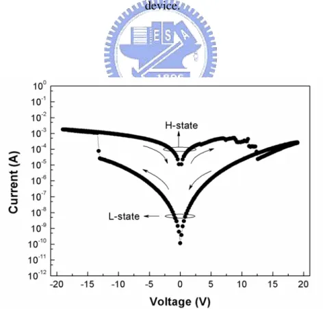
Fig. 4-13 Forming voltage uniformity vs. deposition time and sputtering power. Fig. 4-14 I-V curve of the Al/0.3% V-doped SZO/LNO/Pt device.
Fig. 4-15 Plots of resistance ratio versus bias voltage of theAl/0.3% V-doped SZO/LNO/Pt device.
Fig. 4-16 I-V curve of the Al/0.3% V-doped SZO/LNO structure device. Fig. 4-17 Plots of resistance ratio versus bias voltage of the Al/0.3% V-doped
SZO/LNO device.
Fig. 4-18 Schematic conducting path of (a) four-layer structure, and (b) tri-layer structure.
Fig. 4-19 Current fitting curves of Ohmic conduction. Fig. 4-20 Current fitting curves of F-P conduction.
Fig. 4-21 Hypothetical diagram of the current paths: (a) on process, and (b) off process.
Fig. 4-22 Retention of the Al/0.3% V-doped SZO/LNO/Pt device.
Fig. 4-23 Retention of the Al/0.3% V-doped SZO/LNO/Pt device kept at high temperature.
Fig. 4-24 I-V curve of the Al/0.3% V-doped SZO/LNO/Pt device turned on by -6V, 10ns pulse.
Fig. 4-25 I-V curve of the Al/0.3% V-doped SZO/LNO/Pt device turned on by -4V, 10ns pulse.
Fig. 4-26 Voltage stress of the Al/0.3% V-doped SZO/LNO/Pt device.
Fig. 4-27 Voltage stress of the Al/0.3% V-doped SZO/LNO/Pt device measured at 85oC.
Fig. 4-28 I-V Curves of the Al/0.3% V-doped SZO/LNO/Pt device measured at different temperatures.
Fig. 4-29 Variation of switching voltage of the Al/0.3% V-doped SZO/LNO/Pt device.
Fig. 4-30 Variation of two current state of the Al/0.3% V-doped SZO/LNO/Pt device.
Fig. 4-31 SEM image of cross section of the Al top electrode. Fig. 4-32 SEM image of top view of the Al top electrode.
Fig. 4-33 I-V curves of the Al/0.3% V-doped SZO/LNO/Pt device after
applying 1, 10, 20, 30, 40, and 50th voltage sweeping cycles measured at 150oC.
Fig. 4-34 Variation of two state currents of the Al/0.3% V-doped SZO/LNO/Pt device.
Fig. 4-35 Variation of switching voltage of the Al/0.3% V-doped SZO/LNO/Pt device.
Fig. 4-36 Cross section schematic diagram of the 1D1R device. Fig. 4-37 Read error issue of the device.
Fig. 4-38 I-V curves of the 1D1R device.
Chapter 1
Introduction
1.1 Introduction to Memories
Memory can be classified into two main categories, volatile and nonvolatile memory (NVM).
1.1.1 Volatile Memory
Volatile memory loses its stored data as soon as the system is turned off, so it requires constant power to remain its information. Most types of random access memory (RAM) are in this category. RAM can be subdivided into two main groups, static RAM (SRAM) and dynamic RAM (DRAM). The difference between them is that the stored information of DRAM memory disappears from the memory within milliseconds, so it has to be refreshed periodically. This makes the operation speed of DRAM much slower than that of SRAM. The speed advantage of SRAM means that it is used in cache memory, which is a small amount of high speed SRAM mounted close to or on the processor itself.
1.1.2 Nonvolatile Memory
NVM does not lose its data when the system or device is turned off. A typical NVM device is a MOS-like structure consisting of a source, a drain, an access or a control gate, and a floating gate. It is structurally different from a standard MOSFET in its floating gate, which is electrically isolated. NVMs are subdivided into two main classes, floating gate and charge-trapping. Kahng and Sze proposed
the first floating gate device in 1967 [1]. In this memory, electrons are transferred from the floating gate to the substrate by tunneling through a 3nm thin SiO2 layer.
Tunneling is the process by which an NVM can be either erased or programmed and is usually dominant in thin oxides of thicknesses less than 12nm. Storage of the charge on the floating gate allows the threshold voltage (VT) to be electrically
altered between a low and a high value to present logic 0 and 1, respectively.
In floating gate memory devices, charge or data is stored in the floating gate and is retained when the power is removed. All floating gate memories have the same generic cell structure. They consist of a stacked gate MOS transistor as shown in Fig. 1-1 [1]. The first gate is the floating gate that is buried within the gate oxide and the inter-polysilicon dielectric (IPD) beneath the control gate. The IPD isolates the floating gate and can be oxide or oxide-nitride-oxide (ONO). The SiO2 dielectric
surrounding the transistor serves as a protective layer from scratches and defects. The second gate is the control gate which is the external gate of the memory transistor. Floating gate devices are typically used in electrically programmable read only memory (EPROM), electrically erasable and programmable read only memory (EEPROM), and Flash memory. The disadvantages of NVM are low operation speed, high operation voltage, poor endurance, and its congenital limit in size due to gate oxide thinning that causing poor retention.
1.2 Introduction to Nonvolatile Memory
NVM, such as read only memory (ROM), programmable ROM (PROM), EPROM, EEPROM, and Flash memory, does not lose its data when the system or device is turned off.
1.2.1 Read Only Memory
The very first ROMs are hardwired devices that contain a preprogrammed set of data or instructions. The contents of the ROM have to be specified before chip production, so the actual data can be used to arrange the transistors inside the chip. Hardwired memories are still used, though they are now called masked ROMs to distinguish them from other types of ROM. The primary advantage of a masked ROM is its low production cost. Unfortunately, the cost is low only when large quantities of the same ROM are required.
1.2.2 Programmable Read Only Memory
One step up from the masked ROM is the PROM, which is purchased in an undetermined state. If you look at the contents of an undetermined PROM, you would see that the data is made up entirely of 1's. The process of writing your data to the PROM involves a special piece of equipment called a device programmer. The device programmer writes data to the device one word at a time by applying an electrical charge to the input pins of the chip. Once a PROM has been programmed in this way, its contents can never be changed. If the code or data stored in the PROM must be changed, the current device must be discarded. As a result, PROMs are also known as one-time programmable devices.
1.2.3 Erasable and Programmable Read Only Memory
An EPROM is programmed in exactly the same manner as a PROM. However, EPROMs can be erased and reprogrammed repeatedly. To erase an EPROM, you simply expose the device to a strong source of ultraviolet light. (A window in the top of the device allows the light to reach the silicon.) By doing this, it is practically to reset the entire chip to its initial-undetermined-state. Though more expensive
than PROMs, their ability to be reprogrammed makes EPROMs an essential part of the software development and testing process.
1.2.4 Electrically Erasable and Programmable Read Only Memory
EEPROMs are electrically-erasable-and-programmable. Internally, they are similar to EPROMs, but the erase operation is accomplished electrically, rather than by exposure to ultraviolet light. Any byte within an EEPROM may be erased and rewritten. Once EEPROM is written the new data, the new data will remain in the device forever or at least until it is electrically erased. The primary tradeoff for this improved functionality is higher cost, though write cycles are also significantly longer than writes to a RAM. So EEPROM is used for main system memory.
1.2.5 Flash
Flash memory combines the best features of the memory devices described thus far. Flash memory devices are high density, low cost, nonvolatile, fast (to read, but not to write), and electrically reprogrammable. These advantages are overwhelming and, as a direct result, the use of flash memory has increased dramatically in embedded systems. From a software viewpoint, flash and EEPROM technologies are very similar. The major difference is that flash devices can only be erased one sector at a time, not byte-by-byte. Typical sector sizes are in the range 256 bytes to 16KB. Despite this disadvantage, flash is much more popular than EEPROM and is rapidly displacing many of the ROM devices as well.
1.3 Next-Generation Nonvolatile Memories
Nonvolatile random access memory (NVRAM) is the general name used to describe any type of random access memory which does not lose its information when power is
turned off. This is in contrast to the most common forms of random access memory today, DRAM and SRAM, which both require continual power in order to maintain their data. NVRAM is a subgroup of the more general class of NVM types, and the difference is that NVRAM devices offer random access, as opposed to sequential access like hard disks.
NVRAMs have been investigated for many years, and can be split into to five groups, including semiconductor-oxide-nitride-oxide-semiconductor (SONOS), ferroelectric random access memory (FeRAM), magnetoresistive random access memory (MRAM), phase change random access memory (PCRAM), and resistive random access memory (RRAM).
1.3.1 Semiconductor-Oxide-Nitride-Oxide-Semiconductor
SONOS (as shown in Fig. 1-2) is an old memory concept becoming interesting again, because the present industry standard for NVMs, which is based on charge storage on a floating gate poly, reaches their scaling limits.
SONOS devices trap charge in a nitride layer instead of using a poly-silicon floating gate. The nitride layer is sandwiched between a thin bottom oxide and a blocking oxide. Important for embedded SONOS memories are the lower program and erase voltages compared to floating gate flash, due to the thin bottom oxide. These low voltages are combined with excellent endurance, but the data retention is an issue. The thickness of the top oxide is important to prevent Fowler-Nordheim tunneling of electrons from the gate during erase. To obtain the best compromise between P/E voltage, endurance and retention, the ONO layer optimization is investigated and described in this paper.
The better scaling perspective together with the relative ease of integration in a base line CMOS process and the immunity to stress induced leakage currents makes
SONOS an excellent candidate for embedded flash in the 90 nm node and beyond.
1.3.2 Ferroelectric Random Access Memory
Ferroelectric materials are generally defined by reversible spontaneous polarization in the absence of electric field [2]. The spontaneous polarization is generated from noncentrosymmetric arrangement of ions in unit cell, which produces an electric dipole moment related to the unit cell. Adjacent unit cells are inclined to polarize in the same direction and form a region called a ferroelectric domain. Unit cell of typical ferroelectric material, ABO3, is illustrated in Fig. 1-3 [3]
where A atom, B atom, and oxygen occupy the corner site, body-centered site, and face-centered site, respectively. The ferroelectric materials exhibit a characteristic hysteresis loop as shown in Fig. 1-4 [3]. When an electrical field is applied to the ferroelectric material, the B atom, which has two thermodynamically stable positions inside oxygen octahedra, is displaced relative to the oxygens upward or downward, depending on the polarity of the electric field. This displacement generates a dipole moment inside the oxygen octahedra, which is called as saturated polarization ( Ps). When the applied electric field is removed, the B atom remains
in the displaced position and generates a residual polarization in the absence of applied electric field, or remanent polarization (
±
± Pr). In order to reverse the
direction of polarization, it needs to apply a coercive electric field ( Ec), which is
defined as a minimum electric field for switching the polarization. Therefore, the basic characteristics of a ferroelectric material that make it suitable for NVM applications are its ability to retain two stable remanent polarization values at zero fields, thus providing nonvolatility. The state of polarization can be controlled and sensed by reversing the polarization from up (+1) to down (0) or vice versa as a function of applied voltage.
1.3.3 Magnetoresistive Random Access Memory
In 1988, the physicists found giant magnetoresistance (GMR) effect, and from the effect they learnt the following two things. (1) Spin-dependence scattering can make a significant influence to the total resistance. (2) An interlayer coupling is quite strong between ferromagnetic layers separated by a spacing layer. Thus to investigate the interlayer couplings between ferromagnetic layers across a non-magnetic layer becomes very interesting. One sort of the investigation is tunneling magnetoresistance (TMR) effect. TMR effect is observed on magnetic tunnel junction (MTJ). A MTJ is a layered structure of magnetic and non-magnetic materials. There are many kinds of MTJs, for instance, ferromagnet/insulator /ferromagnet trilayer junction, spin-valve-type junctions with an exchange-biased layer, double and triple barrier layers junctions and so on. Among the various structures they have a common feature that the spacing layer between the ferromagnetic layers is an insulator.
At room temperature (RT), the change of magnetoresistance in GMR is less than that in TMR, so MTJs are often used as the memory cells in MRAM. In a MTJ, the spacing layer which is an insulator is between two ferromagnetic electrodes. One electrode is free to rotate under the external field and the other creates a powerful pinning field to the magnetic layer in one specific direction.
In writing process, the magnetic moment of the free layer is rotated to be parallel or anti-parallel the pinned layer by controlling the two orthogonal magnetic fields. The resistance of the MTJ is lower when the magnetic moments of the free and pinned layer are parallel than the resistance when the moments are anti-parallel. Thus, the parallel and anti-parallel states are arbitrary chosen to present 0 or 1. In general, 0 is corresponding to the parallel state and 1 is corresponding to the anti-parallel state.
In reading process, by passing the current into a MTJ, a low or high resistance is obtained to determine what the data is.
1.3.4 Phase Change Random Access Memory
A phase-change memory array based on chalcogenide materials originally is reported by Neale et al. in 1970. Phase-change materials are often but not always Tellurium-based alloys such as those on the pseudo-binary line (GeTe)x(Sb2Te3)y or
AgInSbTe alloys. They are commonly used in optical data storage in rewritable CD's and DVD's. The operating mode of these materials is based on the change of electronic and optical properties upon a change of the microscopic structure from the crystalline to the amorphous phase [4]-[6]. The electrical conductivity can change by several orders of magnitude upon the phase transition [4], while the optical reflectivity can change depending on layer thickness and wavelength up to 30%. On the other side these alloys represent bad glass formers, in other words that they recrystallize very fast, as soon as they exceed the glass temperature sufficiently. Thus, they can be rapidly switched between the two states, which are why they are called phase change materials.
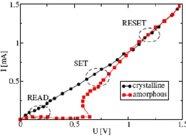
In optical data storage a focused laser beam is applied to switch micron sized bits between the crystalline and the amorphous state. This concept is shown in Fig. 1-5. The information is written by locally melting the crystalline material and rapidly quenching it. This results in an amorphous bit. Erasure is achieved by heating this amorphous region above the crystallization temperature. The current state of a region on the storage device is subsequently read by a laser pulse of low intensity. In the PCRAM's advantage is taken of the change in electric conductivity upon the phase transition from the crystalline to the amorphous structure [7]-[9]. Here the write-read-erase-cycle is affected by an electrical pulse. Figs. 1-6 and 1-7
show the schematic cross section of a PCRAM cell and the corresponding current-voltage curves. The cell is essentially a nonlinear resistor and the readout is performed at low bias (Read region indicated in Fig. 1-7), where the low-field resistance changes by orders of magnitude depending on whether the phase change material in the active region of the device is crystalline or amorphous. To reach the switching regions (SET and RESET shown in Fig. 1-7) the bias is raised above the switching voltage so that enough current can flow through the cell, heating up the active region (Fig. 1-6) resulting in the crystalline-amorphous phase change [10], [11]. At present several manufacturers of RAM chips have initiated research and development projects to explore and use the potential of nonvolatile storage with phase change materials.
1.3.5 Resistive Random Access Memory
a. Introduction to RRAM
Among new NVMs, such as SONOS, MRAM [12], FeRAM [13], PCRAM [14], and RRAM [15]-[16], RRAM shows superior advantages such as simple device structure, low operation voltage, low power consumption, long retention time, small cell size, high operation speed, low cost, good endurance, and non-destructive readout. Its resistive switching phenomenon presents two different current values at the same applying voltage. H-state stands for higher current state and the L-state is lower state. The current states of device can be changed by applying a bias voltage or a voltage pulse. Because the resistance ratio of two current states can reach 3~5 orders of magnitude, it is easy to distinguish two current states by applying reading voltage.
b. Material Groups of RRAM
Resistive switching behaviors have been investigated in PCRAM, doped SrZrO3 (SZO) and SrTiO3 (STO) [17]-[20], binary metal oxide, PrxCa1-xMnO
(PCMO) [21], and organic material [22], [23], and so on. The resistive switching behavior based on current-induced bistable resistance effect or voltage-controlled negative resistance phenomena has been studied in metal/insulator/metal (MIM) structure. The operation voltage of the PCRAM memory cell is large in order to change the phase between the amorphous phase and the crystalline phase. The application limitation of the PCMO device is that the resistance ratio of two current states is too small to be distinguished. In the aspect of the binary oxide materials, they are still unstable and the resistance ratio is not large enough for application. The resistance switching behaviors also have been reported in the polymer thin film, but it has drawback in stability as well as the binary oxide device.
c. The Structure and Operation Method of RRAM
In Fig. 1-8 [16], the RRAM is composed of a transistor and a resistor. In order to write the specific resistor to H-state, a dc voltage is applied on the word line which can turn on the bit transistor and a negative voltage pulse is applied to the bit line while the source of the transistor is grounded in Fig. 1-9 [17]. In order to erase the specific resistor to L-state, a dc voltage is also applied on the word line which can turn on the transistor and a positive voltage pulse is applied on the source of the bit transistor while the bit line is grounded. For the read operation, the word line of the memory cell is selected and a read voltage is applied on the bit line to obtain the current value while the source of the bit transistor is grounded. Therefore, the data comparing the current value with the reference value is determined and do not change the current state of the device during the read operation.
The issue of RRAM is read error. Figs. 1-10(a) and (b) [24] describe how leakage current paths make cell resistance misread. When the resistance is measured with all the unselected lines open, (3,3) cell, for example, has been changed from high to low resistance state after 3 neighboring cells are switched on because of the leakage path described in Fig. 1-10(b). Theoretically this kind of misreading and misprogrammig issues can be avoided by proper biasing method, but the amount of necessary current becomes unreasonably large as memory density increases [25]. Accordingly, it is very important to find suitable rectifying elements to realize an ultra high density cross-point memory device.
1.4 Resistive Switching Properties of Doped SrZrO
3films
In A. Beck’s study [16], [19], he declared that the MIM structure device manufactured with 0.2% Cr-doped SZO films as dielectric layer, SrRuO3 (SRO) and Au
as bottom and top electrode, respectively has resistive switching behavior. The previous research of our lab also uses (100)-oriented LaNiO3 (LNO) which could enhance the
preferred orientation of the SZO films to make 0.2% V-doped SZO films have resistive switching properties [26]. According to Robertsona simulation, Cr, Mn, Fe, V, Co, Cu transition elements, which could provide over two valences in doped SZO thin films, the density of the defects could be modulated by the doping concentration. In addition, the defects are associated with different valences transformed by the applied voltage. Clearly, slight dopant concentration in SZO thin films could induce resistive switching phenomenon, and the V-doped SZO film had better resistive switching behavior. However, the effect of dopant concentration for V-doped SZO film is still unclear. This is because perovskite oxide consists of more than moments, and it’s hard to find optimal recipe to normal manufacturing process because their crystal structure and stoichiometry
are hardly controllable.
From the previous research of our lab, V-doped SZO films deposited on LNO/SiO2/Si substrate have good performance in resistance switching. The resistive
switching of Al/V-doped SZO/LNO device can be operated by bias voltage and voltage pulse. However, the drawbacks of Al/V-doped SZO/LNO device are high operation voltage more than 10V.
In this thesis, the physical and electrical properties of the SZO films deposited by sputter method are reported. The SZO film is deposited on the LNO buffer layer, which is also deposited by sputter method. Pt bottom electrode is deposited on Ti/SiO2/Si
substrate by electron beam evaporation method. Ti deposited by E-Gun is acted as adhesion layer for Pt. Al is evaporated as top electrode by thermal coater. The resistive switching phenomenon can be observed in electrode/resistive thin film/buffer layer/electrode (four-layer) structure.
Four-layer structure compared with electrode/resistive thin film/electrode (tri-layer) structure could enhance the forming voltage, the switching voltage, switching speed, and improving the resistance ratio of two current states. Moreover, based on the current-voltage (I-V) curves and resistive switching phenomena, it is proposed the resistive switching mechanism is local property of SZO films. The conduction mechanisms, reliability, and retention time, are also investigated.
Fig. 1-1 Typical floating gate memory structure.
Fig. 1-3 ABO3 perovskite unit cell [3].
Fig. 1-5 Fundamental concept of the phase change materials.
Fig. 1-6 Schematic plot of a PCRAM cell. Depending on the state of the active region (crystalline or amorphous) the resistance of the cell changes by several orders of magnitude.
Fig. 1-7 I-V curve of a PCRAM cell. SET and RESET denote the switching regions, while READ denotes the region of readout.
Fig. 1-8 Cross section schematic diagram of the RRAM. The transistor is fabricated in the front and the resistor in the back end [16].
Fig. 1-9 Equivalent circuit of an array for the write operation of a given bit resistor [17].
Chapter 2
Experiment Details
2.1 Experiment Process Flow
The experiments are sorted into two parts, including sample preparation and device property analyses as shown in Fig. 2-1.
There are several sample preparation steps as shown in Fig. 2-2. First, 4 inch boron-doped (100) silicon substrates were cleaned by standard RCA clean and then a 200-nm-thick SiO2 layer was thermally grown on the substrates. The SiO2 layer is acted
as the isolation layer to prevent the leakage current from the substrate. Ti deposited by electron beam evaporation is acted as adhesion layer for Pt. Then, Pt bottom electrode layer was deposited on the Ti layer also by electron beam evaporation. Synthesis of the LNO powder and the doped SZO powder were prepared previously. The powders were made to the disk-shaped target for sputtering. After that, the 100-nm-thick LNO films were deposited on the Pt bottom electrode layer to form a (100)-orientated buffer layer by radio frequency (RF) magnetron sputter. Then, the LNO buffer layer was treated by rapid temperature annealing (RTA). After that, the SZO films were deposited on the LNO buffer layer also by the RF magnetron sputter. Finally, 300-nm-thick Al top electrodes were evaporated on the SZO films by a thermal coater. The four-layer structure sample was accomplished and the probe was detected on Al top electrode and Pt bottom electrode as shown in Fig. 2-3.
The device with tri-layer structure was manufactured to be a contrast experiment. A LNO bottom electrode was directly deposited on the SiO2/Si substrate. Besides, all the
depositions, and then, the Al/V:SZO/LNO device was formed as shown in Fig. 2-4. The scanning electron microscope system (SEM) and X-ray diffraction system (XRD) were used to obtain the micro-structure and the crystallization of the films, respectively. XRD analyses were helpful to confirm the orientation of the films. Field emission transmission electron microscope (FETEM) was used to analyze the interface between LNO and SZO films. Focus ion beam (FIB) was used to prepare FETEM sample. Energy dispersive X-ray analyzer (EDS) can analyze the components of LNO and SZO. An Agilent 4155C semiconductor parameter analyzer was used to record I-V curves. By the results of electrical measurement, the manufacturing process was modified to improve the performance of the device.
2.2 RF Magnetron Sputter Systems
In this study, a set of RF magnetron sputter system was utilized to deposit LNO and doped SZO films. The illustration of the sputter system is displayed in Fig. 2-5. The components of the sputter system are indicated as follows.
2.2.1 Vacuum System
It includes a mechanism pump and a diffusion pump. The chamber base pressure was evacuated to 10-5Torr before deposition process. There are several valves to control the atmosphere and the pressure in the chamber and tubes.
2.2.2 Pressure System
There are two digital gauges in the system to present the chamber pressure in different working condition. One is Granville-Phlips Co.’s product with a display range from atmosphere to 0.1 mTorr to show the higher chamber pressure for rough
vacuum or sputtering condition. The other is an ion gauge with an accurate display of a high vacuum from 10-3 to 10-7 Torr. Accordingly, the vacuum situation under sputtering can be precisely controlled and the diffusion pump is working in the safe pressure.
2.2.3 Temperature Controlling System
It contains two thermal couple sensors, a set of four quartz lamps used as heater, and a temperature controller. During the heating process, the lamps just located above the wafer holder could heat the sample directly by radiation in lower pressure. At the same time, the change of the thermal couple could be detected and sent back to temperature controller to modify the heating power. Further, it could help to setup the temperature rising time, holding time, and falling time by a temperature program.
2.2.4 Gas Flow Controlling System
In general, the percentage of oxygen in the sputtering ambience plays an important role in oxide ceramics. Gas mass flow controller (MFC) is used to control the flow rate and atmosphere contents during the sputtering process. Therefore, it could find out that the dependence on the mass ratio of the device performance by tuning recipe.
2.2.5 Plasma Controlling System
This system consists of a RF power generator, a network-matching box, and a 3-inch magnetron gun. The RF power generator has only one working frequency at 13.56MHz, and the network-matching box has minimum reflection power by adjusting the capacitance of the whole circuit. It is able to gain the stable plasma by
the controlling system.
2.2.6 Cooling System
There is cooling water which flows in the pipe welded on the chamber and in the magnetron gun. During the sputtering process, the heating lamps and plasma always produce a lot of redundant heat energy in the chamber, so the cooling water is to prevent from mechanical breakdown and maintain the sample uniformity.
2.3 Preparation of Devices
In the experiment, the four-layer structure device was fabricated. The preparation flow of device is shown in Fig. 2-2.
2.3.1 Preparation of Sputter Targets
Because the LNO and SZO thin films are deposited by the sputter system, it needs two kinds of disk-shaped sputter targets, including the LNO and the doped SZO powder targets.
a. Synthesis of the LaNiO
3Powder Target
The LNO and SZO targets are prepared by the conventional solid-state powder-mixing method. There are six steps in the synthesis processes. First, two kinds of the oxide powders, La2O3 and NiO, were mixed by the rule of
stoichiometry. It should be especially careful of the equivalent mol because 1 mol of the LNO is composed of 0.5 mol of the La2O3 and 1 mol of the NiO. Second, the
mixed powder was put into a jar with anhydrous alcohol and rolling glass balls, and then was mixed adequately by a grinder. Third, the mixture was dried by an 85oC oven. The fourth step was the sintering step. It was the most critical process,
because the sintering temperature and the heating time would affect on the LNO qualities including the resistance and orientation of the LNO sputtered films. The dried mixture was put into a furnace to execute a sequence of sintering, 600oC for 2 hours and 1300oC for 10 hours. In the fifth step, the mixed powder was put in the beaker and baked it in the oven at 150oC for 2 hours. Finally, the mixed powder put in the disk-shaped target was squeezed by a high pressure of 2000 pounds for 60 seconds such that a compact target was produced for sputtering work. The preparation flow of the LNO target was showed in Fig. 2-6.
b. Synthesis of the SrZrO
3Powder Target
The SZO powder was synthesized from two kinds of oxide powder, SrCO3 and
ZrO2. In order to substitute Zr atom, it was considered the suitable ionic radius
compared with Zr atom. Considering all the conditions, transition metaloxide V2O5
was added to form the doped SZO powder. Because V has freakyoxidation number, it could show more effect on the electric properties of ourmemory thin films. For example, when it is expected to synthesize 0.3%V dopedSZO powder, it should use 1 mol of SrCO3, 0.997 mol of ZrO2, and 0.0015mol of V2O5. After mixing above
elements of the doped SZO powder, the same steps were followed as synthesis of LNO powder. The mixed powder was put into a furnace of a sequence of sintering process. In the last step, adisk-shaped target was made by a high pressure of 2000 pounds for 1 min.The manufacturing process was showed in Fig. 2-7.
2.3.2 Thin Film Depositions
The LNO bottom electrode and the doped SZO films were deposited by RF magnetron sputter sequentially. To meet our demands for different process recipe, several parameters were controlled to deposit the films based on the plasma theorem
and the models of the thin film growth. There were many parameters including the chamber pressure, the RF power, the working temperature, the ambient conditions, and the deposition time. In general, chamber pressure affected the mean free path (MFP) of plasma which is relative to the deposition rate. The lower pressure was choice to create the larger MFP in the chamber, which leads to the higher deposition rate. Moreover, the deposition rate is dependent on the RF power as well. In the experiment, while depositing both the LNO and doped SZO films, the RF power was set 100 or 150W and the chamber pressure at 10 mTorr. In addition, the temperature and the ambient condition could have influence on the density of the defects, the crystallization, the conductivity, the stoichiometry, and the dielectric constant of thin films.
For the accuracy of the atmosphere, it needs the base pressure about 3×10⁻⁵ Torr before sputtering. Next, to maintain the ambient condition, the flow rate of Ar and O2 by MFC was controlled, and the working pressure was kept by the valves
among low pressure where the plasma was generated.
2.3.3 Heat Treatment after Thin Film Depositions
There were two purposes for the experiment using the RTA systems. One is in order to get stronger crystallization orientation or better conductivity of the LNO buffer layer. The other is to control the properties of our sample by changing RTA atmosphere (O2 or N2) or the heating profile of RTA temperature. The RTA model
was FE-004A made by JETFIRST.
2.3.4 Deposition of the Top Electrode
Before the Al top electrodes were deposited on the doped SZO films, the sample had been adhered to a metal mask. The metal mask had different hole with
three kinds of diameters that are 150, 250, and 350μm. So the different areas are defined for the top electrodes, which are 1.767×10⁻⁴, 4.908×10⁻⁴, and 9.612×10⁻⁴ cm2.
Al used as the top electrode was deposition by a thermal evaporation coater (EBX-6D) manufactured by ULVAC. The samples were loaded with metal masks on the spinning holder, which made the deposition rate more uniform. Then, the rough pump and the turbo pump would work in term in order that the base pressure before deposition reached 5×10⁻⁶ Torr.
2.4 Measurements and Analyses
2.4.1 X-Ray Diffraction
Generally, thin films are classified according to its crystallization. There are three types of crystallization, including amorphous, polycrystalline, and crystalline. XRD analysis was used to investigate the crystal structure and orientation of our sample. Furthermore, the crystallization dependence of the samples could be identified for heat treatment. In the experiment, the thin films were grown between amorphous type and poly type. By Scherrer’s formula, 0.9
cos D B λ θ × = × , this could estimate the average grain size from XRD illustration. Where the background information of the XRD analysis is that λ =1.5405Å (Kα), B is the full width at half
maximum (FWHM) of the XRD peak and θ is the diffraction angle. In this analysis, X-ray was made with 0.02 degree beam divergence and operation configuration at 30KV, 20mA.
2.4.2 Scanning Electron Microscope
Comprehensively, the surface morphology issue is also a quite important character compared with the character of bulk for the thin films. The surface micro-morphology and cross section of our sample could be observed by SEM analysis. Besides, the crystallization of the thin films needed to be investigated directly by XRD analysis. So, SEM analysis is helpful to get enough information to support our illustration. The SEM model is S4700I with high resolution of 15Å made by Hitachi.
2.4.3 Focus Ion Beam
FIB is a scientific instrument that resembles a scanning electron microscope. However, the SEM uses a focused beam of electrons to image the sample in the chamber, whereas a FIB instead uses a focused beam of gallium ions. Gallium is chosen because it is easy to build a gallium liquid metal ion source (LMIS). In a Gallium LMIS, gallium metal is placed in contact with a tungsten needle and heated. Gallium wets the tungsten, and a huge electric field (greater than 108V per centimeter) causes ionization and field emission of the gallium atoms.
Unlike an electron microscope, the FIB is inherently destructive to the specimen. When the high-energy gallium ions strike the sample, they will sputter atoms from the surface. Gallium atoms will also be implanted into the top few nanometers of the surface, and the surface will be made amorphous.
Because of the sputtering capability, the FIB is used as a micro-machining tool, to modify or machine materials at the micro- and nano-scale.
The FIB is commonly used to prepare samples for the transmission electron microscope. The TEM requires very thin samples, typically ~100 nanometers. The nanometer-scale resolution of the FIB allows the exact thin region to be chosen.
2.4.4 Field Emission Transmission Electron Microscope and Energy
Dispersive X-Ray Spectrometer
The state-of-the-art JEOL JEM-2100F field emission transmission electron microscope is equipped with an Oxford INCA Energy TEM 200 EDS (energy dispersive X-ray spectrometer) system, a Gatan GIF Tridiem EELS (electron energy loss spectrometer) system and a Fischione high-angle annular dark field detector. Features of the JEM-2100F include a high-brightness Schottky field emission electron gun producing a probe size of less than 0.2 nm. Ultra-high point-to-point TEM resolution is 0.19 nm; atomic scale resolution of 0.136 nm can be achieved using high angle annular dark field (HAADF) scanning transmission electron microscopy (STEM) imaging. The facilities are ideally suited for crystallographic and chemical analyses at a sub-nanometer scale, including high-sensitivity EDS and EELS.
Both EDS and EELS are analytical TEM (ATEM) techniques and can provide elemental composition and distribution information. The Oxford INCA Energy TEM 200 EDS system has the following features: automatic peak ID and labeling; element maps and linescans using SmartMap data acquisition; ability to define a line or grid of points for automatic data acquisition; absorption correction for samples of finite thickness and Sitelock image drift correction.
2.4.5 Scanning Probe Microscopy
SPM has enabled researchers to image surfaces at the nanometer scale. Rather than using a beam of light or electrons, SPM uses a fine probe that is scanned over a surface (or the surface is scanned under the probe). By using such a probe, researchers are no longer restrained by the wavelength of light or electrons. The
resolution obtainable with this technique can resolve atoms, and true 3-D maps of surfaces are possible. SPM is a general term, used to describe a growing number of techniques that use a sharp probe to scan over a surface and measure some property of that surface.
2.4.6 Current-Voltage Measurements
The most important part of all is current-voltage measurement. It could understand the electrical properties of the device from current-voltage curve. The electrical measurement system consisted of a probe station, an Agilent 4155C semiconductor parameter analyzer, an Agilent E5250A low leakage switch which are controlled by personal computer with the Agilent VEE software, and GPIB controller.
Our electrical measurements were sorted into five items, static conductivity switching measurement, retention test, stress test, endurance test, and other electrical phenomenon measurement. The aforementioned four items were tested for criteria of our memory device and the last item was executed to understand the fundamental mechanism of our samples.
a. Static Resistive Switching Measurement
The measurement was performed by Agilent 4155C which applied a dc voltage sweeping between two specified voltages to observe the resistive switching of the sample. The measured results could observe the relation of the switching voltage and the H-state or L-state current. Use Agilent 4155C to execute the double voltage sweep function, current-voltage curve was determined with two different-current states associated with the positive applied voltage or the negative one.
b. Retention Test
Retention time is the time of information keeping. The data (1 or 0) is not able to be distinguished beyond retention time. The current of the sample in the H-state or L-state was measured after fixed period. The retention time of the V-doped SZO film was very long. By applying the higher temperature on the device, the retention test is accelerative.
c. Non-Destructive Readout Test
The sample stressed smaller voltage than the switching voltage was able to stay in the same conductivity state. The smaller positive and the smaller negative sweep voltage were applied on the sample all the time and observed that the current changed with sweeping cycles.
d. Endurance Test
The device applied the enough voltage (positive or negative voltage) was able to change the resistance between two states. Of course, the resistance ratio of the device increased after repeat sweeping cycles. The phenomenon, which was the decrease of the H-state current and the increase of the L-state current, was useful for us to explain the conduction mechanism.
Fig. 2-1 Illustration of the experimental flow.
(100) Si substrate RCA
Oxidation (200nm SiO2)
Deposition of Pt-Ti bottom electrode by electron beam evaporation
Deposition of LNO buffer layer
RTA for LNO buffer layer Deposition of SZO resistive layer
Deposition of Al top electrode
Fig. 2-3 Cross section of the four-layer structure device.
Fig. 2-5 Illustration of the sputter system.
La2O3 NiO
Mixed and ball-milled in the absolute alcohol for 24hr and dried at the 85oC oven
Heated at 600oC for 2hr and then baked at 1300oC for 10hr
Ball-milled in the absolute alcohol for 24hr and dried by the 150oC oven for 2hr
SrCO3 ZrO2
Mixed and ball-milled in the absolute alcohol for 24hr and dried by the oven
Heated at 600oCand 800oC for 2hr and then baked at 1250oC for 10hr
Ball-milled in the absolute alcohol for 24hr and dried by the oven
Heated at 600oCand 800oC for 2hr and then baked at 1400oC for 10hr
Ball-milled in the absolute alcohol for 24hr and dried by the oven
Dopant oxide
Chapter 3
Possible Mechanisms of Conductivity Switching Phenomenon
Generally speaking, the basic conduction mechanisms in insulating films are Schottky emission, Frenkel-Poole emission, Tunneling or field emission, Space-charge-limited current, Ohmic conduction and Ionic conduction. The summary of mathematical expressions and voltage versus temperature dependence of these mechanisms are listed in Table. 3-1 [27]. These basic mechanisms are explained briefly as follows.
(1) Schottky emission corresponds to the thermionic emission induced carrier transport across the metal-insulator interface or the insulator-semiconductor interface.
(2) Frenkel-Poole (F-P) emission is caused by field-enhanced thermal excitation of trapped electrons into the conduction band. The expression of trap state is virtually identical to Schottky emission, but the barrier height is instead of the depth of trap potential well. The barrier lowing is twice as large as Schottky emission one because of the immobility of the positive charge.
(3) Tunnel or field emission is due to the current induced by electrons tunneling from the metal fermi-energy into the insulator conduction band.
(4) Space-charge-limited current is caused by the current that result from the carriers injected into insulator didn’t be recombination with any compensating charge. (5) Ohmic conduction corresponds to the electrons that hop from one isolated state to
the next by thermally exciting, that usually happen in low voltage and high temperature condition.
(6) Ionic condition presents ions can’t be readily injected or extracted from the insulator. Positive and negative space charge will build up near interface after an initial current flow. In addition, hysteresis effect happens result from residual
internal field caused some ions to flow back their equilibrium position when the applied voltage is removed.
At present, there are more and more reports to study the possible mechanism of RRAM deeply based on these basic mechanisms. Many researchers illustrate their opinions for the source of conductivity switching characteristics from various materials. From these reports, the possible mechanism could be sorted into six species shown in follows.
(1) Conducting filament (2) Charge transfer
(3) Storage and release of charge carrier
(4) Dipole rearrangement induced polarization (5) Phase transformation
(6) Formation of the depletion layer
The possible mechanism will be introduce and analyze in the following sections.
3.1 Conductance Filament [16], [28]-[33]
The conducting filament is a theory that one or several conducting paths are formed in the dielectric layer by field such that conductivity is changed. This conducting channel can be divided into two kinds that one is composed by metallic elements (ohmic mechanism), and the other is composed by defects.
Metallic filament will be “line up” to form a conducting path inside the insulator when a voltage is applied on the device. That is H-state (high conductivity). In contrast, when the voltage is applied to the H-state device, this path will be broken and the conductivity will be back to initial low conductivity. This is L-state (low conductivity). It is noteworthy that these metallic atoms may come from the electrodes or just are neutral
impurities in the insulator. However, the conductivity should increase with decreasing temperature in two cases. In addition, with applying further positive pulses, the area of the conducting path may increase, but thus newly appearing path would be less conducting than that formed on the first pulse, because most of the current injected by the electric pulse flows through the first conducting path and has much less effect on the other area. Therefore, the dc resistance, which is primarily dominated by the most conducting path, does not change very much with further applying electric pulses.
A defect configuration which is consisting of alternate anions and cation vacancies was also proposed. It is reasonable that conduction then take place by hopping between adjacent localized anion sites; besides, this model would be the (more or less) one dimensional analogue, furthermore, might satisfactorily account for the low activity energy. The other condition is that when voltage is applied, the conductivity increases to form H-state due to clusters or domains connecting, and then the resistance value will be lower than original one. Reversing the pulsed field could reshape the clusters and rearrange them into a secondary organized state to form another conductivity state.
3.2 Charge Transfer [15]
In general, defects or impurities in insulator will form energy states between energy gaps, thus one can utilize various dopants to induce different acceptor and donor levels. According to A. Beck’s statement, energy levels can be formed by doping transitional elements into insulator film. After applying a voltage pulse, the transitional elements may change their valences because of unsteadiness of transitional elements. Hence, the donor or acceptor level is also changed, and mobile electrons are induced. On the other hand, the transitional elements will restore to its original valences through an opposite polarity of voltage. In conclusion, charge transfer process via donor and acceptor level as
studied by photocurrent and luminescence measurements appear to be a possible mechanism for carrier creation and transport in insulator.
3.3 Storage and Release of Charge Carriers [17], [21], [34], [35]
The concept of this mechanism is that charge carriers trapped and detrapped process will induce current in insulator. It is much similar to charge stored and released in the floating gate flash memory. Besides, this mechanism can be divided into “bulk effect” and “interface effect” i.e., two sorts.
The impurity band of charge transport level is deep charge-trapping level or emission (recombination) center. At H-state, the transport levels or the traps are uncharged. At low voltages, charge is injected primarily from one of the electrodes and moves through the transport states. At voltages in the negative differential resistance region, charges tunnel into the trapping sites and a space-charge field builds up, which opposes the field applied at the injecting electrode and reduces the current to form the L-state. If the voltage is rapidly reduced to zero, charge is left in the traps and forms an electrical field. When applying another smaller voltage again to the device this field will reduce the applied field and induce lower current flow. In contrast, by applying opposite direction voltage, the trapped charge will be drawn out and back to H-state.
Some reports suggest interface electrochemistry between electrode and insulator, such as oxygen vacancy creation/diffusion, should be responsible to the switch phenomenon. Besides, the higher field and defect density may be as a result of the relatively high mobility that is observed. That is so-called electrical oxidation and reduction charge transfer. This behavior also implies a process of charge stored and released in insulator happens because electrical oxidation means an element gets electrons and electrical reduction means it loses electrons.
3.4 Dipole Rearrangement Induced Polarization [36], [37]
This mechanism with conductivity switching character is attributed to its materials have a permanent dipole moment inside. When a voltage is applied, the disorder dipoles in local ranges will be rearranged along electrical field direction and form the first conductive state. By applying opposite polarity voltage, the dipoles can be rearranged along opposite electrical field direction to form another conductive state. This mechanism is usually proposed to be the conductivity change origin in ferroelectric and some organic materials. There are a large number of researches about FeRAM application associated with its hysteresis curve. On the other hand, some investigations also prove ferroelectrics have reversible conductivity switching phenomenon due to its polarization reversal. For example, conductivity switching character is observed in ultra-thin ferroelectrics film such as PZT and bulk single crystal ones such as LiNbO3.
3.5 Phase Transformation [4]-[6], [9], [10], [14], [38], [39]
The concept of this mechanism is the focus on the conductivity of poly-crystal film is higher than it of amorphous film. The typical case is OUM (Ovonic Unified Memory) that is manufactured by chalocogenide material. One can control different temperature and heating time to cause different phase. Thus, by controlling pulse voltage width, that means different heated gradient result in different phase (different conductivity). It is noticeable that the polarity of pulse voltage has no affection on crystalline phase (no difference on conductivity). The crystalline phase is only varied through different pulse voltage width.
3.6 Formation of the Depletion Layer [40]
The depletion region is formed with a layer of unscreened dopant ions. It is clear that Schottky barriers will be set up at electrode and insulator interface. In some investigations, the device manufactured by organic or polymer insulator with reversible conductivity reveals its capacitance change with applying voltage. Because when a positive voltage is applied to the device, some negative carriers or ions will drift to near interface region, and by applying negative voltage will attract positive ones to near interface region.
Table3-1 Basic conduction mechanisms in insulators [28].
Conducting mechanism Voltage and temperature dependence
Schottky emission ~ 2exp( a V q B)
J T T kT Φ + − F-P emission J ~ exp(V 2a V q B) T kT Φ + − Tunneling (field) emission ~ 2exp( 1)
J V
V
−
Space-charge-limited current ~ 2
J V
Ohmic conduction J ~ exp(V 1)
T
−
Ionic conduction J ~V exp( 1
T T )
−
Chapter4
Results and Discussion
4.1 Properties and Analyses of the LaNiO
3Buffer Layer and SrZrO
3Resistive Films
According to the previous studies, the Al/0.3% V-doped SZO/LNO structure device has resistive switching performances [26]. But the switching voltage of the tri-layer structure device is over than 10V. It is proposed due to the low conductivity of the LNO bottom electrode. Large amount of applied voltage drops on the LNO bottom electrode causing to the high operation voltage. In order to reduce the operation voltage, several methods are used to enhance the conductivity of the LNO bottom electrode, such as the RTA process of the LNO, controlling the sputtering parameters for the LNO, different bottom electrode used to replace the LNO, Al/0.3% V-doped SZO/LNO/Pt structure (four-layer structure), and so on. Among these methods, four-layer structure device has different resistive switching properties and best performance. Therefore, this thesis is focus on the resistive switching properties of the four-layer structure.
4.1.1 X-Ray Diffraction and Scanning Electron Microscope Analyses of
the LaNiO
3Buffer Layer
In accordance with the previous studies, the Al/0.3% V-doped SZO/LNO structure device had good resistive switching properties while the preferred orientations of the SZO film are (100) and (200) [26]. At this study, the LNO electrode in four-layer structure becomes a buffer layer to deposit particular orientations or the crystallization of the upper layer, and the LNO film has similar
physical properties to the upper layer, which will improve the crystallization of the upper resistive layer. Besides, dependent on the previous studies, the LNO film has many advantages as listed in follows.
(1) It has (100) and (200) preferred orientations rather than (110), so the better electrical properties of the SZO film on the LNO film can be anticipated.
(2) The LNO film could efficiently crystallize at about 250oC, where has the advantage of the low temperature CMOS process in the future.
(3) The cost of LNO is much cheaper than other noble metals.
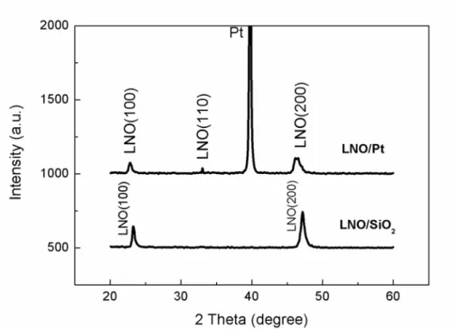
If the SZO film was directly deposited on Pt or other metals, such as Al, Ti, Ta, Zr, Ni, and Nb, no (100)-preferred orientation film can be obtained, and no good resistive switching behaviors can be observed [26]. Instinctively, the characteristics of the LNO buffer layer could influence the properties of the memory devices. Fig. 4-1 shows the expected crystallization of the LNO buffer layer grown on the Pt bottom electrode. It has (100) and (200) preferred orientations rather than (110). It shows that the crystallization of LNO buffer layer in four-layer structure is almost identical to that in tri-layer structure. Then, the expected crystallization of the V-doped SZO film was grown on the LNO film. The device is expected to have good resistive switching properties.
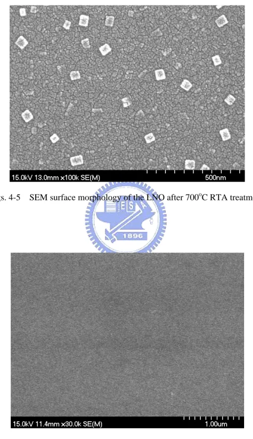
Fig. 4-2 shows surface micro-morphology of the as-deposited LNO buffer layer. The sputter-deposited LNO buffer layer is flat and uniform.
A thermal treatment was added to improve the properties of the LNO buffer layer before the deposition of doped SZO film. The crystallization orientation or better conductivity of the LNO buffer layer can be controlled by changing RTA ambience or the heating profile of the RTA temperature, and high RTA temperature process is also utilized to test the thermal stability of LNO buffer layer. From the
![Fig. 1-10 Describing how leakage current paths make cell resistance misread [24].](https://thumb-ap.123doks.com/thumbv2/9libinfo/8123255.165977/33.892.174.747.545.1053/fig-describing-leakage-current-paths-make-resistance-misread.webp)
![Table 4-3 Resistive switching properties of the SZO-, TiO 2 -, and PCMO-based devices [15], [41]-[46]](https://thumb-ap.123doks.com/thumbv2/9libinfo/8123255.165977/72.892.140.756.918.1152/table-resistive-switching-properties-szo-pcmo-based-devices.webp)