應用於超寬頻系統之低雜訊放大器之設計
78
0
0
全文
(2) 應用於超寬頻系統之低雜訊放大器之設計. Design Low Noise Amplifier for Ultra- Wideband Application 研 究 生:王柏之. Student:Po-Chi Wang. 指導教授:郭建男. Advisor:Chien-Nan Kuo. 國 立 交 通 大 學 電 子 工 程 系 電子研究所碩士班 碩 士 論 文. A Thesis Submitted toInstitute of Electronics College of Electrical Engineering and Computer Science National Chiao Tung University In partial Fulfillment of the Requirements For the Degree of Master In Electronics Engineering June 2004 Hsinchu, Taiwan, Republic of China. 中華民國九十三年六月.
(3) 應用於超寬頻系統之低雜訊放大器之設計. 學生: 王柏之. 指導教授: 郭建男教授 國立交通大學 電子工程學系 電子研究所碩士班. 摘要 本篇論文主旨在於利用標準 0.18um CMOS 製程設計適用於超寬頻系統前端接受器之 低雜訊放大器積體電路。此外,使用達靈頓對架構之窄頻低雜訊放大器亦被設計與分 析。此兩顆低雜訊放大器已經由晶片製作而被驗證。 第一顆晶片在於設計與分析一適用於 5-GHz 頻帶無線區域網路之高增益低雜訊放 大器。此放大器使用達靈頓對之兩倍截止頻率之特性來達到高增益之目的。實驗結果顯 示此一放大器在 6GHz 頻率有著最高功率增益(S21) 15.5dB,輸入返回損耗(S11) -12 dB 以及最低雜訊指數 3.5dB,此外此電路消耗之功率為 13mW。 在第二顆晶片裡,適用於接收端超寬頻系統之寬頻放大器被設計與分析。我們利用 負回受電阻達到寬頻之輸入阻抗匹配以及自偏壓,增益補償方法達到操作頻率範圍內之 平坦增益,進而濾除操作頻率範圍外之訊號。實驗結果顯示此一放大器在 3-8 GHz 頻率 下有著最高功率增益(S21) 9.2dB,輸入返回損耗(S11)低於 -5.8dB 以及平均雜訊指數 6.1dB,此電路消耗之功率為 15mW。此外,改善性能之超寬頻放大器已被製作,並且加 入了可變增益之功能以增加輸入信號動態範圍。. i.
(4) Design Low Noise Amplifier for Ultra-Wideband Application Student: Po-Chi Wang. Advisor: Prof. Chien-Nan Kuo. Department of Electronics Engineering & Institute of Electronics National Chiao-Tung University. ABSTRACT The aim in this thesis is mainly based on the design of low noise amplifier (LNA) in the receiver path of ultra-wideband system using standard 0.18um CMOS process. Also, a narrow band LNA using Darlington pair structure is designed for 5.5-GHz frequency band. The two low noise amplifiers were verified through 2 individual chips. In the first chip, a narrow band high gain low noise amplifier using Darlington pair structure is analyzed and designed for wireless local network area (WLNA) operating at 5-GHz frequency band. We employ the double cutoff frequency property of Darlington pair to achieve high gain design. Measured data show that the amplifier achieves maximum power gain (S21) of 15.5 dB, -12 dB input return loss (S11), and minimal noise figure of 3.5 dB at the 6GHz frequency while consuming 13mW. In the second chip, a wideband amplifier (LNA), intended for use in the receiver path of an ultra-wideband (UWB) system, is analyzed and designed. We employ the techniques of negative feedback resistors to achieve broadband matching together with self-biasing, and gain compensation method to derive flat gain over the entire operating frequency band as well as filter out the signal out of band. Measured data show that the amplifier achieves maximum ii.
(5) power gain (S21) of 9.2 dB, input return loss (S11) below -5.8 dB, and average noise figure of 6.1dB in the frequency range from 3 to 8-GHz, while consuming only 15mW. The improved and modified version in terms of the measured result from this chip has been implemented. Also, variable gain function has been added to enlarge the input dynamic range in the modified chip.. iii.
(6) 誌謝 終於完成這篇論文,首先要感謝我的指導教授郭建男博士這一年半以來給我的指導 與鼓勵,不但讓我在射頻積體電路設計的領域中獲益良多,並且對積體電路設計又更深 入的了解與認識。再者,感謝實驗室每一位同學這一年半的照顧與提攜,在這實驗室裡 不僅讓我學習到了做學問的方法以及對專業領域深入的研究,更讓我交到了一堆志同道 合的好朋友,這是我這段時間除了學問外所獲得的最大資產。另外,亦要感謝國家晶片 中心(CIC)以及洪英瑞同學在晶片製作與量測上的大力幫忙,使得我能更順利的完成此 篇碩士論文。最後更要感謝我的家人給我精神上與經濟上的支持,特別是我母親的栽培 與鼓勵使我能夠順利完成碩士的生涯。其他要感謝的人還有很多,不可剩數,在此一併 謝過. iv.
(7) CONTENTS ABSTRACT (CHINESE) …................................................i ABSTRACT (ENGLISH) ...................................................ii ACKNOWLEDGEMENT …………………………..........iv CONTENTS……...................................................................v TABLE CAPTIONS.............................................................ix FIGURE CAPTIONS............................................................x Chapter 1 Introduction………………………………….....1 1.1 Motivation………………………………………………...........1 1.2. Thesis Organization……………………………………….........2. Chapter 2 Low Noise Amplifier Basic Concepts..............3 2.1 Noise in MOSFET……………………......................................3 2.1.1 Source of Noise…………………………………………….........3 2.1.1.1. Drain Noise......................................................................................4. 2.1.1.2. Gate Noise........................................................................................4. 2.1.1.3. Flicker Noise....................................................................................7. 2.1.2 Noise Models of the MOS Transistors…………………...............7. v.
(8) 2.2. Low Noise Amplifier Basic……………………………………8 2.2.1 Low Noise Amplifier Topology and Basic…..…………... …….8 2.2.2 Inductive Source Degeneration LNA…………………………..11 2.2.2.1 Operational Basic.............................................................................11 2.2.2.2 Optimizations of LNA Design Flow………………………………14. 2.2.3 Introduction to Broadband LNA……………………………….18. Chapter 3. 5.5 GHz High Gain LNA Using Darlington Pair………………………..............................22. 3.1 Motivation………………………………………….................22 3.2. Analysis of Darlington Pair LNA Topology………………….22 3.2.1 Design principle…..…………………………………................22 3.2.2 Analysis and Design of the LNA Using Darlington Pair............24 3.2.2.1 Trans-conductance in Darlington Pair Stage....................................24 3.2.2.2 Input Impedance Matching………………………………………..25. 3.3 Discussion on Simulation and Measurement Result…………26 3.3.1. Verification of Equation(3-4)...…………………...…................26. 3.3.2. Chip Implementation…………………………………...............29. 3.2.3 Simulation and Measurement Result…………………………...29. 3.4. Conclusion…………………………………………………….33. vi.
(9) Chapter4. A 3 to 8GHz Ultra-Wideband CMOS LNA………………………………………….34. 4.1 Introduction…………………………………………………..34 4.2 Principle of the circuit design…………………………...........34 4.2.1 Ultra-Wideband LNA Circuit Topology……………………….34 4.2.2. Broadband Input Matching…………………………………….36. 4.2.3 Gain Flatness Technique……………………………………….37 4.2.4 Design Considerations and Trade Off………………………….39. 4.3 Chip Implementation and Measured Result………………….40 4.3.1 Microphotograph of Chip………………………………............40 4.3.2 Measurement and Simulation Result…………………………...41. 4.4. Improved UWB LNA…………………………………...........45 4.4.1. Wide-band Input Matching………………………......................46. 4.4.2. Variable Gain Function…………………………………............48. 4.4.3 Simulation Result……………………………………….............52 4.4.3.1 Noise Figure......................................................................................52 4.4.3.2 S-Parameter………………………………………………………...53 4.4.3.3 Linearity……………………………………………………………56 4.4.3.4 Summary of Performance and Comparison with other Wideband Amplifier………………………………………...............................57 4.4.3.5 Chip Photograph…………………………………………………...58. vii.
(10) 4.4.4. Chapter5. Conclusion……………………………………………………..59. Summary and Future Work......……………61. 5.1 Summary………………………………….…………………..61 5.2. Future Work………………………….………………………62. REFERENCES......…………………………………..........63 VITA……………………………………………………….65. viii.
(11) TABLE CAPTIONS Table Ⅰ Summary of simulation and measured result of Darlington pair LNA and comparison with single input MOS……………………………………………..33 Table Ⅱ Summary of measured result of the Ultra Wide-band LNA and performance comparison to other wideband amplifier………………………………................45 Table Ⅲ Simulation. result. and. specification. of. the. modified. ultra. wide-band. LNA........................................................................................................................58 Table Ⅳ Summary of performance comparison with other wideband amplifier……………58. ix.
(12) FIGURE CAPTIONS Fig .2.1. Drain current noise model..........................................................................................4. Fig .2.2. (a) Gate noise circuit model (b) its equivalent voltage noise model..........................5. Fig .2.3. Flicker noise model………………………………………………………………….7. Fig .2.4. (a) MOSEFET noise model (b) equivalent input referred noise model……………..7. Fig .2.5. Common LNA architecture (a) Resistive termination (b) 1/gm termination (c) shunt-series feedback, and (d) inductive degeneration………………..................9. Fig .2.6. (a) Common source input stage (b) input stage of ISD LNA noise model………...11. Fig .2.7 Configuration of an N-stage distributed amplifier………………………................18 Fig .2.8. Configuration of shunt-series amplifier…………………………………................20. Fig .3.1. Schematic of Darlington pair low noise amplifier………………………................23. Fig .3.2. Cutoff frequency of device m1, m2 and M1 versus drain current…………………..27. Fig .3.3. Profit (M) versus total current of input stage……………………………................27. Fig .3.4. Influence of miller effect on the S21………………………………………………..28. Fig .3.5 Microphotograph of the Darlington LNA circuit…………………………................28 Fig .3.6 Simulation and measured result of power gain (S21) and isolation (S12)…………..30 Fig .3.7 Simulation and measured result of input match……………………………………..31 Fig .3.8 Simulation and measured result of output match…………………………................31 Fig .3.9 Simulation and measured result of noise figure……………………………………..32 Fig .3.10 Measured result of two-tone test at 5 GHz…………………………………………..32 Fig .4.1. Schematic of Ultra Wide-band LNA………………………………………………35. Fig .4.2. Small signal analysis of ultra wide band LNA…………………………………….36. Fig .4.3 Illustration of signal amplification………………………………………………….37 Fig .4.4 Microphotograph of the UWB LNA circuit………………………………………..41 Fig .4.5. Simulation and measured result of power gain (S21) and isolation(S12)................43 x.
(13) Fig .4.6. Simulation and measured result of input match and output match………………..43. Fig .4.7. Simulation and measured result of noise figure…………………………...............44. Fig .4.8 Measured result of two-tone test at 5 GHz; Measured IIP3 versus frequency............44 Fig .4.9 Schematic of the modified UWB LNA……………………………………………..46 Fig .4.10 Modified input matching network to improve S11 at high frequency in band.. ……………………………………………………………………………................47 Fig .4.11 Using mutual inductance to reduce spiral inductor area…………………………….47 Fig .4.12 Simulation result of the transformer-like spiral inductor……………………………48 Fig .4.13 Illustration of variable gain method…………………………………………………50 Fig .4.14 The variable gain tank Gload………...……………………………………………….50 Fig .4.15 Simulation result of variable gain function…………………………………...……..51 Fig .4.16 Simulation result of Noise Figure…………………………………………………....52 Fig .4.17 Simulation result of power gain (S21) at different control voltage………………….53 Fig .4.18 Simulation result of power gain (S21) versus different control voltage at different frequency…………………………………………………………………..54 Fig .4.19 Simulation result of voltage gain without the buffer stage…………………………..54 Fig .4.20 Simulation result of reverse isolation S12…………………………………...............55 Fig .4.21 Simulation result of input return loss (S11) at different control voltage……………..55 Fig .4.22 Simulation result of output return loss (S22) at different control voltage…...............56 Fig .4.23 Simulation result of two-tone test at 5 GHz………………………………………….57 Fig .4.24 Simulation result of IIP3 versus frequency…………………………………………..57 Fig .4.25 Photograph of the modified UWB LNA……………………………………………..59. xi.
(14) CHAPTER 1 INTRODUCTION 1.1. Motivation Wireless communications at multi-gigahertz frequencies are a huge market that drives. the semiconductors technology toward low-cost solutions. CMOS technology, which is attractive due to its advantages of low cost, high-level integration, and enhancing performance by scaling [1, 2], will meet the market requirement in system implementation. Typically, the first stage of a receiver is a low noise amplifier (LNA), whose main function is to provide enough gain to suppress the noise of subsequent stages as well as adding as little noise as possible in itself. The major problem of CMOS technology at high frequencies is the low amplification as result of parasitic capacitance and conducting silicon substrate. Hence, to derive enough signal amplification and low noise contribution of a low noise amplifier using CMOS technology often involves high power consumption. How to provide enough gain in a low noise amplifier (LNA) suitable for a specific wireless communication system without consuming too much power is the main object of this thesis. In the thesis, two low noise amplifiers intended for the receiver path of 5.8-GHz wireless LAN and Ultra-Wideband System are analyzed, designed and implemented. In the first one for narrow band application, popular inductive source degeneration architecture for the first stage of the LNA is replaced with Darlington pair combined with modified matching network. Under input matching condition, the Darlington pair acts as a current amplifier at the operating frequency to provide larger amplification compared to inductive source degeneration architecture under same dc current consumption. In the second one for Ultra-Wideband system, the gain compensation method to derive flat gain over the entire frequency band is designed to redeem the tradeoff between gain, 1.
(15) bandwidth and power consumption. Also, a variable gain function between 3 and 8 GHz to enhance the dynamic range of the input signal is added to the second improved UWB LNA circuit.. 1.2 Thesis Organization In the Chapter 2 of the thesis, some theoretical MOSFET noise model and noise theory are introduced. Although these basic concepts provide a guidance to design a low noise amplifier, it is not enough to design a superior fully on-chip CMOS LNA including the consideration of some other important figure of merit such as gain, power consumption etc. . A systematic LNA design method associated with CMOS process is developed earlier [3] and represented in this chapter. In the Chapter 3, a narrow band LNA using Darlington pair structure intended for application of the 5-GHz wireless LAN is introduced. The detailed circuit analysis and design equation is presented. Circuit simulation and comparison with single-ended inductive source degeneration topology are also discussed. Finally, measurement result of the LNA chip fabricated by TSMC 0.18um CMOS technology is discussed. In the Chapter 4, a 3 to 8-GHz wideband amplifier intended for UWB system is proposed. The gain flatness technique using frequency compensation method to derive flat gain over the entire frequency band is introduced. The combination of negative feedback resistor and inductive source degeneration network is designed to achieve input matching. Also, some design consideration and trade-off is discussed. The measured data and simulation result of the circuit is compared and discussed. Finally, based on the measurement result of this chip, a second modified version is designed to achieve better performance. Also, the variable gain function is added to the circuit. In the last chapter, all the work is summarized and concluded. 2.
(16) Chapter 2 Low Noise Amplifier Basic Concepts In this Chapter, some theoretical MOSFET noise model and noise theory are presented in section 2.1. Although these basic concepts provide a guidance to design a low noise amplifier, it is not enough to design a superior fully on-chip CMOS LNA including the consideration of some other important figure of merit such as gain, power consumption etc.. In section 2.2, a systematic narrow band LNA design method associated with CMOS process developed earlier [3] is discussed. Finally, some broadband LNA architecture is discussed in section 2.3. 2.1 Noise in MOSFET To develop good CMOS RF circuit design skills, a fundamental understanding of noise source in a MOSFET is necessary. Noise can be roughly defined as any random interference unrelated to the signal of interest, which can be sorted out interference noise and inherent noise. Interference noise results from interaction between circuit and outside world, or between different parts of the circuit itself. Interference noise can be reduced by carefully circuit layout and wire routing. On the other hand, inherent noise originates from the fundamental property of the circuit itself and it can be reduced but never eliminated. Inherent noise is only moderately affected by circuit layout, such as using multiple finger number to reduce the gate resistance of a MOSFET. However, inherent noise can be significantly reduced by proper circuit design, such as choosing circuit topology and increasing power consumption.. 2.1.1 Source of Noise 3.
(17) In this section, we will focus on the inherent noise of a MOSFET, which can be categorized into three parts: drain noise, gate noise and Flicker noise, mainly.. 2.1.1.1 Drain Noise The dominant noise source in a MOSFET is the channel noise, which basically is a thermal noise originated from the voltage-controlled resistor mechanism of a MOSFET. Thus, one would expect noise commensurate with the resistance value. Indeed, detailed theoretically considerations lead to the following expression for the channel noise of a MOSFET, which is 2. modeled as a shunt current noise “ ind “in the output current of the device, as shown in Fig.2.1: drain 2 ind = 4kT γgd0 ∆f. (2-1). 2 ind. source Fig.2.1 drain current noise model Where gd0 is the zero-bias drain conductance of the device, and γ is a bias dependence factor. In long channel device, the value of parameter γ is unity at zero drain-source voltage, and decreased to 2/3 when device is saturated. Unfortunately, γ is much greater than 2/3 for short channel device operating in saturation. This excess noise is originated from carrier heating by large electric field in short channel device. This value would worsen the noise performance as the technology proceeds.. 2.1.1.2 Gate Noise In addition to channel noise, the thermal agitation of channel charge has another important consequence: gate noise. If the MOSFET are biased so that channel operates in the inverted condition, fluctuations in channel charge will induce physical current in the gate due to capacitive coupling. Although this noise can be neglected at low frequencies, it dominates. 4.
(18) at radio frequencies. The companion effect of the gate noise that occurs at high frequencies arises due to its ‘distributed’ nature of the MOSFET. As operating frequency approaches cutoff frequency ωt of a MOSFET, the gate impedance of the device exhibits a significant phase shift from it purely capacitive value at lower frequencies. This shift can be accounted for a real, noiseless conductance, gg, in the gate current. Thus, the circuit model to represent the gate noise is the current noise connected between gate and source terminal shunted by a conductance gg, as shown in Fig.2.2 (a). Van der Ziel [4] has shown that the gate noise may be expressed as. 2 ing = 4kT δg g ∆f. (2-2). where the parameter gg gg =. ω 2 C 2gs 5g d 0. and the typical value of the coefficient of gate noise “δ”, equal to 3/4 in long channel device while 4 to 6 in short channel one. The gate noise current clearly has a power spectral density that is not constant. In reality, gate noise increases as frequency increases, so it is often called “blue noise” to continue the optical analogy. For those who prefer not to analyze a system that has no blue noise source, it is possible to recast the model in a form with a noise voltage source that possesses a constant power spectral density. The alternative model can be derived first transform the parallel RC network into equivalent series RC network. If one assumes gate. gate 2 ing. source. gg. rg. 2 v ng. C gs. source. (a). C gs. (b). Fig.2.2 (a) Gate noise circuit model (b) its equivalent voltage noise source model. 5.
(19) high Q of the network, then the capacitance C would roughly not change during the transformation, while the parallel resistance becomes a series resistance whose value is. rg =. 1 1 1 1 1 ⋅ 2 ≈ ⋅ 2 = gg Q + 1 gg Q 5g d 0. (2-3). which is independent of frequency. Finally, equate the short circuit currents of the original network and the transformed version, the equivalent voltage noise source is then found to be 2 v ng = 4kTδrg ∆f. (2-4). which possesses a constant power spectral density. Hence, the final noise model contains a voltage noise source in series with a equivalent resistance whose value is not dependent on the frequency as shown in Fig.2.2(b). Because the two noise source do share a common origin, they are also correlated, that is, there is a component of the gate noise current that is proportional to the drain current on an instantaneous basis. The correlation between gate and drain noise can be expressed mathematically as follows [4]:. c≡. * ing ⋅ ind 2 2 ing ⋅ ind. = 0.395 j. (2-5). where the value of 0.395j is exact for long channel devices. The correlation can be treated by expressing the gate noise as the sum of the two components, the first of which is fully correlated with the drain noise, and the second of which is uncorrelated with the drain noise. Hence, the gate noise is re-expressed as 2. 2. 2 ing = 4kTδgg (1 − c )∆f + 4kTδgg c ∆f. (2-6). where the first term is uncorrelated and the second term is correlated to drain noise. Because of the correlation, special attention must be paid to the reference polarity of the correlated component. The value “c” is positive for the polarity shown in Fig.2.2 (a). 6.
(20) 2.1.1.3 Flicker Noise Charge trapping and releasing by the defects and impurities on the interface between thin oxide and channel are usually invoked to explain the flicker noise (1/f noise). Since a MOSFET is surface device, it would exhibit more 1/f noise than bipolar device. One means of comparison is to specify a ‘corner frequency’, where the flicker noise is equal to the thermal noise. A lower corner frequency means less total noise. In RF circuit design, it is not important to care about flicker noise in bipolar devices, whose corner frequency often below tens or hundreds of hertz, while MOSFET often exhibit 1/f corners of tens of kilohertz to a megahertz or more. For a MOSFET, the 1/f noise can be represented by a drain current noise connected between drain and source terminal as shown in Fig2.3, and its value is drain i12/ f =. gm2 K K ⋅ ⋅ ∆f ≈ ⋅ ω2T ⋅ A ⋅ ∆f 2 f WLC ox f. i12/ f. (2-7) source. Fig.2.3 Flicker noise model where “A” is the area of the gate(=WL) and K is a device-specific constant. For NMOS device, K is typically about 10-28 C2/m2, whereas for PMOS devices it is about 50 times larger. From the first equation above, one can observe that larger dimension size and thinner dielectric exhibit less 1/f noise, because larger gate capacitance smoothes the fluctuations of the channel charge. For the second equation, one can see the 1/f would worsen as technology proceeds because of the positive proportional dependence on the cutoff frequency (ωt).. 2.1.2. Noise Models of the MOS Transistors From previous introduction of noise source, a standard MOSFET noise model is. G v. S. 2 rg. Rg. i. 2 ngu. i. +. 2 ngc. C gs. v gs. −. Fig.2.4(a) MOSFET noise model 7. D g m v gs. ro. 2 ind. S.
(21) noiseless network. G 2 v neq. Rg. 2 ineq. D. + v gs. C gs. ro. g m v gs. −. S. S Fig.2.4 (b) equivalent input referred noise model. 2 2 presented in Fig.2.4. In Fig.2.4 (a), ind is the drain current noise, and ing is the gate current 2. 2 2 noise, which is separated into correlated ( ingc ) and uncorrelated ( ingu ) terms. Also, vrg is added. to represent the noise originated from the parasitic resistor of gate terminal, which may be due to the gate resistor of the device or the parasitic resistor of the input inductor. Also, we have neglected the effect of gg under the assumption that the gate impedance is largely capacitive at the frequency of interest. Here, the noise model also can be represented as a noiseless network together with two equal noise sources ( veq2 and ieq2 ) in Fig.2.4 (b). The relationship between two equivalent models is as follows. v. 2 neq. =v. 2 Rg. 2 ind + i ⋅ R + 2 ⋅ (1 + ω 2 C 2gs R 2g ) gm 2 ng. = 4kT (R 2g + δg gR 2g +. 2 2 2 ineq = ingc + ingu +. (2-7). 2 g. γg d 0 ⋅ (1 + ω 2 C 2gs R 2g ))∆f 2 gm. 2 ind γg ⋅ ω2C2gs = 4kT(δgg + 2d0 ⋅ ω2C2gs )∆f 2 gm gm. (2-8). 2.2 Low Noise Amplifier Basic In this section, we discuss some LNA architecture, and introduce the most popular architecture, inductive source degeneration topology [3].. 2.2.1 Low Noise Amplifier Topology and Basic In the design of low noise amplifiers, there are several common goals. These include minimizing. the. noise. figure. of. the. amplifier,. 8. providing. gain. with. sufficient.
(22) linearity—typically measured in terms of the third-order intercept point, IP3—and providing a stable 50Ω input impedance to terminate an unknown length of transmission line which delivers signal from the antenna to the amplifier. A good input match is even more critical when a pre-select filter precedes the LNA because such filters are often sensitive to the quality of their terminating impedances. The additional constraint of low power consumption which is imposed in portable systems further complicates the design process. The first work of designing LNA circuit is to provide stable input impedances. Here, the four basic architectures are illustrated in simplified form in Fig 2.5. Each of these architectures may be used in a single-ended form, or in a differential form. Note that differential form will require the use of a balun or similar element to transform the single-ended signal from the antenna into a differential signal. Practical baluns introduce extra loss which adds directly to the noise figure of the system.. Zin. Zin. (b). (a). Zin. Zin. (c). (d). Fig.2.5 Common LNA architecture (a) Resistive termination (b) 1/gm termination (c) shunt-series feedback, and (d) inductive degeneration 9.
(23) The first technique uses resistive termination of the input port to provide a 50Ω impedance. There are two effects to degenerate the noise performance of the amplifiers. First, the added resistor contributes its own noise to the output which equals to the contribution of the source resistance. Second, the input is attenuated by the added input resistance. The larger noise penalty resulting from these effects therefore makes this architecture unattractive for the more general situation where a good input termination is desired. A second approach uses the source of the common-gate stage as the input termination, is shown in Fig 2.5(b). A simplified analysis of the common-gate architecture, assuming matched conditions, yield the following lower bounds on noise factor for the cases of and CMOS amplifiers CMOS:. F = 1+. γ 5 ≥ = 2.2(dB) α 3. where the γ is the coefficient of the channel thermal noise and α is the ratio of the device trans-conductance gm and zero-bias drain conductance gd0 . In the short-channel device, α is smaller than one and γ is greater than one due to hot electrons in the channel. Above the previous analysis, the minimum theoretically achievable noise figure tend to be around 2.2dB or greater practically. The third architecture of the amplifiers is shunt-series feedback, as illustrated in Fig 2.5(c). In this topology, input-matching and output-matching network can be achieved by using shunt and series feedback resistances. However, the amplifiers using that shunt-series feedback usually have high power dissipation compared to other types of low noise amplifiers. The higher power consumption is partially owing to the fact that shunt-series amplifiers are wideband ones. In many applications, such as GPS, GSM, a wideband front end is not required and it is able to make use of the narrowband structure to reduce power. For this reason, the shunt-series feedback method is not applied in the narrow band design. The Forth architecture utilizes inductive source degeneration impedance as represented in Fig 2.5(d) to generate a real term in the input impedance. The narrow band matching can get good power 10.
(24) performance as well as better tuning of the input matching of amplifiers. This technique is not only used in the narrow-band wireless communications, such as GPS or GSM receivers, but also employed for ultra-wideband system, which we will introduce in Chapter 4. In the following section, the discussion of low noise amplifier will focus on the inductive source degeneration structure.. 2.2.2 Inductive Source Degeneration LNA In 1997, Thomas H. Lee and Derek K. Shaeffer suggested a popular method to optimize the noise performance of the inductive source degeneration (ISD) LNA [3]. In the section, the noise optimization on the inductive degeneration topology under gain and power constraint is discussed.. V DD Vbias. 2 iout. M2 Lg. Lg. M1. Rs. Rg. v rg2. + v gs 2 ingc C gs −. 2 i ngu. Zin Ls. v s2. g m v gs. 2 ind. Ls. (a). (b). Fig.2.6 (a) Common source input stage (b) input stage of ISD LNA noise model 2.2.2.1 Operational Basic and noise figure calculation Selecting the first stage of a LNA is a very important thing for obtaining good noise and input matching. The topology of the cascode LNA with ISD and the equivalent circuit for input stage noise calculation are shown in Fig 2.6(a) and Fig 2.6(b). In Fig 2.6(a), the input impedance of the cascode amplifier is represented by. 11.
(25) Zin = s(L g + L s ) + = ωTL s. g 1 + ( m )L s sCgs Cgs. (ω = ω0 =. 1 (L g + L s )Cgs. (2-9) ). where we obtain the input impedance Zin is equal to the multiplication of cutoff frequency of the device and source inductance at resonant frequency, this value will be set to 50Ω for input matching. In Fig 2.6(b), Rg represents the series resistance of the inductor as well as the gate resistance of the NMOS device, and while the. 2 ingc. and. 2 i ngu. 2 ind. represents the channel thermal noise of the device,. are the gate noise with correlated and uncorrelated term. Here, analysis. based on this circuit neglects the contribution of subsequent stages to the amplifier noise figure. This simplification is justifiable provided that the first stage possesses sufficient gain and permits us to examine in detail the salient features of this architecture. Then recall the noise figure for a circuit is defined as: NF =. Total _ output _ noise Total _ output _ noise _ from _ the _ source. (2-10). To find the output noise, we first evaluate the trans-conductance of the input stage. With the output current proportional to the voltage on Cgs and nothing that the input circuit takes the form of series-resonant network, the trans-conductance at the resonant frequency is given by G m = gm Q in =. ωT gm = ω 0 C gs (R s + ω T L s ) 2ω 0 R s. (2-11). where Qin is the effective Q of the amplifier input circuit. From this equation, the output noise power density due to the source is S a,srce (ω0 ) = S src (ω0 )G m2 ,eff =. 4kT ω 2T ω L ω02R s (1 + T s ) 2 Rs. (2-12). In a similar way, the output noise power density due to Rg can be expressed as 12.
(26) 4kTR g ω 2T S a,Rg (ω0 ) = ω L ω02R 2s (1 + T s ) 2 Rs. (2-13). Next, the noise power density associated with the correlated portion of the gate noise and drain noise can be expressed as S a,id ,ig ,c (ω0 ) =. 4kT γκg d0 ω L (1 + T s ) 2 Rs. (2-14). where ⎡ δα 2 κ = ⎢1 + c Q L 5γ ⎢⎣ 1 QL = ω 0 R s C gs α=. 2. ⎤ δα 2 2 c ⎥ + 5γ ⎥⎦. gm g d0. The last noise term is the contribution of the uncorrelated portion of the gate noise. This contributor has the following power spectral density: S a,id ,u ( ω 0 ) = ξS a,id ( ω 0 ) =. where. ξ=. 4kT γξ g d0 ω L (1 + T s ) 2 Rs. (2-15). δα 2 2 (1 − c )(1 + Q L2 ) 5γ. We observe that the equation (2-14) and (2-15) can all proportional to the power spectral density of drain current noise, then the two equation can be combined as a simplified form: S a,M1 (ω0 ) =. 4kTγχg d0 ω L (1 + T s ) 2 Rs. (2-16). where χ is defined as χ = 1+ 2 c QL. δα 2 δα 2 2 + (1 + Q L ) 5γ 5γ. According to (2-10), (2-13) and (2-16), the noise figure at the resonant frequency can be written by the following equation:. 13.
(27) NF =. S a,source (ω0 ) + S a,Rg (ω0 ) + S a,M1 (ω0 ) S a,source (ω0 ). = 1+. Rg Rs. +. γ χ α QL. ⎛ ω0 ⎜⎜ ⎝ ωT. ⎞ ⎟⎟ ⎠. (2-17). To understand the implications of this new expression for F, we observe that χ includes terms which are constant, proportional to QL, and proportional to QL2. It follows that (2-17) will contain terms which are proportional to QL as well as inversely proportional to QL. Therefore, a minimum F exits for a particular QL.. 2.2.2.2 Optimizations of LNA Design Flow So far, we have analyzed the noise performance of the input stage of an inductive source degeneration topology. This analysis can now be drawn upon in designing the LNA. Besides noise performance, gain and power dissipation are another important considerations in LNA circuit design. In this subsection, how to pick the appropriate device width and bias point to optimize noise performance given specific objectives for gain and power dissipation is our goal. To quantify these terms, a simple second-order model of the MOSFET transconductance can be employed which accounts for high-field effects in short channel devices. Assume that drain current Id has the form I d = WC ox v sat. ( Vgs − VT ) 2. (2-18). ( Vgs − VT ) + Lε sat. where Cox is the gate oxide capacitance per unit area, νsat is the saturation velocity, and εsat is the velocity saturation field strength. To simplify the following analysis, (2-18) can be reformulated as Id = WC ox v sat. η2 1− η. where we define η =. (2-19). Vgs − VT ( Vgs − VT ) + Lε sat 14.
(28) Because the device M1 must operate in saturation region, the range of overdrive should be within:. 0 ≤ Vgs − VT ≤ Vds. (2-20). Hence, the parameter η should be within the range 0≤η≤. Vds Vds + Lε sat. (2-21). Having established an expression for Id, we can formulate the power consumption of the amplifier as follows: PD = VddId = Vdd WC ox v sat. η2 1− η. (2-22). To differentiate (2-18), we can determine the trans-conductance of device M1. gm =. ∂Id = WC ox v sat (2η − η 2 ) ∂Vgs. (2-23). From (2-22), we can derive the cutoff frequency of the device M1 gm 3v sat [ − (η − 1) 2 + 1] ωT ≈ = C gs 2L. (2-24). Here, we have assumed that gate-source capacitance is equal to (2/3)WLCox, and the gate-drain capacitance(Cgd) have been neglected. Substituting (2-23) into (2-11) gives Gm =. 3 v sat [ − ( η − 1) 2 + 1] 4L ω 0 R s. (2-25). This expression shows that the trans-conductance of the input stage is only dependent on the bias condition and frequency of operation given specific technology and source resistance, while the power dissipation not only depend on bias condition but also on the gate width of device M1 as shown in (2-22). Finally, substituting (2-24) into (2-17) gives. 15.
(29) n +l W + F = 1+ Rs − ( η − 1) 2 + 1 mW +. Rg. where m =. n=. l=. (2-26). 4 γ L2 C ox δα 2 2 ( ω 0 R s )(1 + ) 9 α v sat 5γ. δα 5R s C ox v sat. 4 γ 2 ω 0L c 3 α 2 v sat. The expression shows that a minimum F exits for a particular width W, and the higher the bias point, the lower the F. There are two approaches to this optimization problem which deserve special attention. The first assumes a fixed trans-conductance, Gm, for the amplifier. The second assumes fixed power consumption. Now, we review the two different conditions using the equation we have developed. 1) Fixed Gm optimization: To fix the value of the trans-conductance, Gm, we need only assign a constant value to η. Once η is determined, we can minimize the noise factor by taking ∂F =0 ∂W. (2-27). which, after some algebraic manipulations, results in. Wopt,Gm =. n 3 5γ ⎞ ⎛ = ⋅ ⎜1 + ⎟ m 2ω0R sLC ox ⎝ δα 2 ⎠. −1. (2-28). The optimal width will gives the minimal noise factor given that bias condition has been determined by Gm. Finally, the power consumption is determined by the optimal width and bias condition. In this approach, the main advantage is that designer can choose the trans-conductance of input stage arbitrary to achieve high gain and low noise performance. 16.
(30) The disadvantage is that we sacrifice the power consumption to achieve noise performance. 2) Fixed PD Optimization: An alternative method of optimization fixes the power dissipation and adjusts width, W, and bias point, ρ, to minimize the noise factor. Under fixed power consumption PD, we re-express noise factor as: 1− η η2 j + l] + 1− η η2 F = 1+ − (η − 1) 2 + 1 [i. where i =. j=. l=. 4 γ L2 C ox PD δα 2 PD 2 ω + m = ( R )( 1 ) 0 s v sat E sat VDD 5 γ VDD 9 α v 2sat E sat. VDD LE sat δα VDD LE sat n= PD 5R sPD. 4 γ 2 ω 0L c 3 α 2 v sat. after some algebraic manipulations by taking. ηopt = Wopt =. (2-29). ∂F = 0 , results in ∂η. 1 + l 2 + 12ij 2j. (2-30). 1 − η opt PD 2 Vdd C ox v sat η opt. (2-31). where we have assumed η << 1 .Given fixed power constraint, the minimal noise factor is. determined by (2-30) and (2-31). Finally, the Gm has been designed under the optimal bias condition, ηopt. In this approach, the main advantage is that designer can specify the power dissipation and find the optimal low noise performance. The disadvantage is that the trans-conductance of the input stage is held up by the optimal noise condition. From (2-11) and (2-17), we found that the cutoff frequency of the input device determine the gain and noise performance of the inductive source degeneration LNA. As CMOS process technology continues to improve, the higher gain and lower noise. 17.
(31) performance may be expected. Now, device cutoff frequency, fT , is bounded within any given technology, so it would seem that once biasing conditions that maximize fT have been established, the designer has done all that can be done. However this facile conclusion overlooks the possibility of topological routes to increasing fT. In chapter Ⅲ, an alternative inductive source degeneration LNA using Darlington pair input stage to double fT is discussed and implemented.. 2.2.3 Introduction to Broadband LNA Ultra wideband (UWB) systems are a newly wireless technology capable of transmitting data over a wide spectrum of frequency bands with very low power and high data rates. Although the UWB standard (IEEE 802.15.3a [5]) has not been completely defined, most of the proposed applications are allowed to transmit in a band between 3.1 and 10.6 GHz. How to design a low noise amplifier suitable for the receiver path of the UWB system becomes a challenge for RF circuit designer. In general, this type of amplifier would have constant gain and good input matching over the desired frequency bandwidth, and provide low enough noise figure while consuming power as little as possible.. Ld. Zd. Input. Lg. Ld. Lg. Ld. Lg. Ld. Lg. Output. Zg. Fig.2.7 Configuration of an N-stage distributed amplifier With recent advances in RF integrated circuit and device processing technology, 18.
(32) distributed amplifiers (DAs) were widely used to realize broadband amplifier [6-8]. The basic configuration of DAs is shown in Fig 2.7. A cascade of N identical FETs have their gates connected to a series inductors, Lg , while the drains are connected to a series inductors, Ld. The combination of gate-source capacitance(Cgs) of each device and the series inductors, Lg, forms a approximate transmission line with characteristic impedance Zg’ ( Lg / C gs ) equal to. Zg. If the Zg is equal to 50Ω, the approximate transmission line will give good input matching to 50Ω. In the same way, the output matching will be achieved. In amplification aspect, the input signal propagates down the gate line, with each FET tapping off some of the input power. The output signals amplified by the trans-conductance of FETs form a traveling wave on the drain line. The inductors (Ld’s) are chosen for constructive phasing of the output signals, and the termination impedances on the lines serve to absorb waves traveling in the reverse directions [9]. In CMOS technology, Bandwidths extending to tens of giga-hertz of DAs are possible, with good input and output matching. Distributed amplifiers can not achieve very high gains or very low noise figure, however, and generally are larger in size because of many on-chip inductors. The main drawback on the DAs is that power consumption is generally large owing to several stages cascaded to derive an adequate gain level. Also, the bandwidth of the DAs basically is a low pass filter, whose excess amplification below 3.1 GHz would distort the wanted signal for ultra-wideband application. An alternative approach to the design of broadband amplifiers is to use negative feedback [10]. One particularly useful broadband circuit that employs negative feedback is the shunt-series amplifier as shown in Fig 2.8. With the assistance of negative feedback resistor, the Rin and Rout can be matched to 50 easily in low frequency. Formally, Rin and Rout is given by. 19.
(33) RE ( RF + RL ) RE + RL. Rin =. (2-32). Rf. Rout. RL. Rs Rout =. RE ( R F + RS ) RE + RS. Rin RE. (2-33). Fig.2.8 Configuration of shunt-series amplifier. Comparing the expressions for input and output resistance, we see that if Rs and RL are equal (as is commonly the case) then Rin and Rout will also be precisely equal. This happy coincidence is one reason for the tremendous popularity of this topology. Unfortunately, the presence of gate-source capacitance, Cgs , and Miller-augmented gate-drain capacitance, Cgd , which appear between gate and ground, makes it impossible to achieve perfect input impedance matching at high frequency. These effects can be mitigated to a certain extent by using L-match network to transform the resistive part up to the desired level. Of the possible types of L-matches, the best choice is usually one that places an inductance in series with the gate and a shunt capacitance across the amplifier input; such a network becomes transparent at low frequencies, where no correction is required. After some assumption and calculation, we can derive the relationship between voltage and bandwidth: ⎛ C gs Rs C gd BW ⋅ Av ≈ ⎜⎜ + 2 ⎝ gm. ⎞ ⎟⎟ ⎠. −1. (2-34). This topology trades gain for bandwidth, so amplifier bandwidths in excess multi-gigahertz using CMOS technology are possible at the expense of gain and noise figure. From previous discussion, we found that a broad band amplifier generally suffers from two problems: low gain and power hungry. The first problem would degrade noise performance on the following stage in the receiver path, and the second one would not be 20.
(34) suitable for general portable device. In section 2.2.2, we have known that inductive source degeneration architecture possess near-optimum noise performance [3], and high gain potential in term of cutoff frequency of input MOS device, while dissipating less power than broad band amplifier. In Chapter 4, we will utilize these advantages of inductive source degeneration combined with the resistive feedback technique to design a wideband amplifier suitable for the UWB system.. 21.
(35) CHAPTER 3 5.5 GHz High Gain LNA Using Darlington Pair. 3.1 Motivation We have introduced the inductive source degeneration topology to design LNA in section 2.2.2. From (2-11) and (2-17), we found that the cutoff frequency of the input device determines the gain and noise performance of the inductive source degeneration LNA. As CMOS process technology continues to improve, the higher gain and lower noise performance may be expected. Now, device cutoff frequency, fT , is bounded within any given technology, so it would seem that once biasing conditions that maximize fT have been established, the designer has done all that can be done. However this facile conclusion overlooks the possibility of topological routes to increasing fT. In this chapter, an alternative inductive source degeneration LNA using Darlington pair input stage to increase fT is analyzed and implemented.. 3.2 Analysis of Darlington Pair LNA Topology 3.2.1 Design principle In section 2.2.2, we have derived the trans-conductance of an inductive source degeneration LNA input stage as shown in (2-11). Now, we rewrite and reconsider this equation. G m,M1 = gm Q in =. gm ωT = ω0 C gs (R s + ωT L s ) 2ω0R s. (3-1). we can reformulate this equation as ωT gm β = = Gm,M1 = ω0 C gs (R s + ωT L s ) ω0 (R s + Z in ) R s + Z in. ( ω = ω0 ). (3-2). where β is the current gain of the input stage, which is proportional to the cutoff frequency 22.
(36) of the input device and inverse proportional to the frequency of operation, and the Zin is the input impedance of the input stage. Eq.(3-2) stands for the trans-conductance of the input stage is proportional to the current gain itself at the operating frequency under input matching condition. In other words, the input stage acts as a current amplifier at the frequency of operation. If we can increase the current gain of the input stage without changing the input matching condition, we will get larger trans-conductance to derive more gain and suppress noise of the subsequent stage at the operating frequency.. Ld output. m3. Cs. C pass. Cp. input m1. Zin. L g1. Z1 m2. Lg 2. Rl. Fig 3.1 Schematic of Darlington pair low noise amplifier. 23.
(37) 3.2.2 Analysis and Design of the LNA using Darlington Pair Because Darlington pair has approximate double cutoff frequency [10], it means that Darlington pair has larger current gain. Now, the Darlington pair topology has been employed to replace the input stage of our designed LNA circuit as shown in Fig 3.1. The Lg1 and Lg2 are designed to achieve input matching, and cascode common-gate device m2 for less Miller’s effect and better reverse isolation. The resistor, Rl, is designed for biasing. Because the value of Rl is large enough compared to Z1 at operating frequency, the bias resistor would not affect the normal operation of the Darlington Pair. Also, Ld1, Cs and Cp are designed for output matching, while Cpass for local small signal ground.. 3.2.2.1 Trans-conductance in Darlington Pair Stage To analyze the trans-conductance of input stage, we neglect the contribution of subsequent stages and the overlap capacitance Cgd. The use of a cascoded first stage helps to ensure that this approximation will not introduce serious errors. After some small signal calculation, the trans-conductance of the Darlington pair at operating frequency gives ⎛ ⎞ ⎛ gm1Cgs2 + gm2 Cgs1 ⎞ gm1gm2 ⎟ − j⎜ ⎟ GDAR = − ⎜ ⎜ 2Z ω 2 C C ⎟ ⎜ 2Z s ω0 Cgs1Cgs2 ⎟ ⎠ ⎝ s 0 gs1 gs2 ⎠ ⎝ 2. ⎛ ωt1ωt 2 ⎞ ⎛ ωt1 + ωt 2 ⎞ ⎜ ⎟ +⎜ ⎟ ⎜ ω 2 ⎟ ⎜ ω0 ⎟ ⎠ ⎝ 0 ⎠ ⎝ ≈ 2Z s. (3-3). 2. where the ωt1 and ωt2 are the cutoff frequency of the m1 and m2 devices, respectively. Also, we have assumed input impedance matching to Rs. To compare the trans-conductance of the Darlington pair and a single device, (3-1) and (3-3) were combined as 2. ⎛ ω ω ⎞ ⎛ ω + ωt2 ⎞ G ⎟⎟ M = DAR = ⎜⎜ t1 t 2 ⎟⎟ + ⎜⎜ t1 Gm ⎝ ωt ω0 ⎠ ⎝ ωt ⎠. 2. (3-4) 24.
(38) where the M means the profit using Darlington pair compared to single device. To gain more insight of the profit, we consider the following case. If we roughly assumed that ω T ∝ PD and ω T 1 = ω T 2 = G DAR ≈ 1 . 8 G m. and PD ( darlington ) =. ωT , we can derive the following result 2. PD 2. (3-5). where we have assumed the frequency of operation is 5 GHz, and the cutoff frequency (ωT) is 30 GHz, a typical value in 0.18um CMOS process. More detailed will be simulated in Section 3.3.1.. 3.2.2.2 Input impedance matching The configuration of inductive source degeneration topology provides impedance matching to 50Ω with the help of source inductor (Ls). To derive input matching to 50Ω in the Darlington pair topology, an inductor Lg2 is inserted between the source of the device m1 and the gate of the device m2 as shown in Fig 3.1. A portion of Lg2 (Lt) is designed to tune out the gate-source capacitance of device m2, while the remainder serves as the inductive source degeneration inductor (eq. Ls) of device m1 for input matching. The analysis is shown as follows. Z 1 = sL g2 + = sL s. Z in = sL g1 + ≈ ωTL s. 1 1 = s(L t + L s ) + sC gs 2 sC gs 2. (3-6). (at resonance ) 1 + Z in2 sC gs1. (3-7). (at resonance). 25.
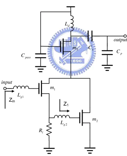
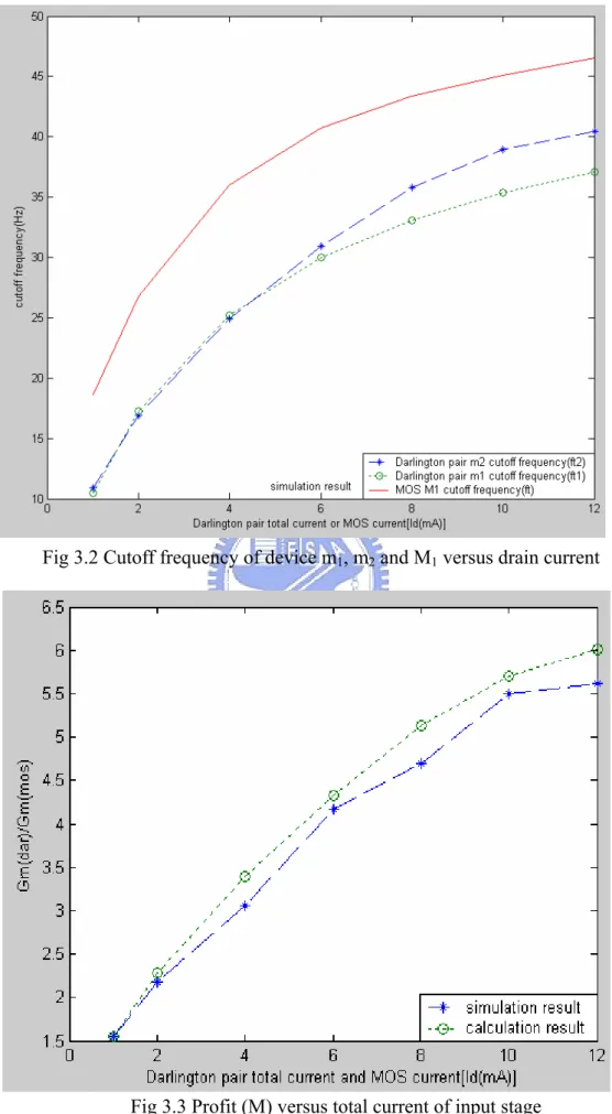
(39) 3.3 Discussion on Simulation and Measurement Result 3.3.1 Verification of Equation (3-4) The 0.18um RF CMOS model provided by the TSMC is employed to simulate and verify the validity of equation (3-4). Here, we have assumed the drain current of device m1 and m2 are one half of that of the single device. In other words, the total current consumed by Darlington pair is equal to that of a single device. Now, we find out the cutoff frequency of every device (m1, m2 and M1) under the specified bais condition, the result is shown in Fig 3.2. Finally, we substitute the cutoff frequency for the (3-4), and compared it to the simulated result, as shown in Fig 3.3. The calculation result of (3-4) agrees well with the simulated result. Thus, the validity of (3-4) is verified. Also, we find under the same current consumption the trans-conductance of Darlington pair is 1.5 to 6 times larger than a single device. This means, we can use the Darlington pair to derive larger trans-conductance without dissipating too much power compared to a single device. In previous verification, we have assumed the output load of the input stage is zero. Unfortunately, the cascoded stage still hold low input impedance, this would degrade the trans-conductance of the input stage due to Miller effect. Because the Darlington pair has larger trans-conductance, it would result in larger voltage gain from output to the input compared to the single device under the same cascoded input impedance. In Fig 3.4, we saw the trans-conductance degradation of Darlington pair is larger than that of single device due to Miller effect. Here, we have assumed the cascoded stage is an ideal current buffer with a low impedance 20Ω (a typical value of 0.18um NMOS) and the output of the cascoded stage has been matched to 50Ω.. 26.
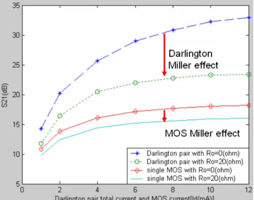
(40) Fig 3.2 Cutoff frequency of device m1, m2 and M1 versus drain current. Fig 3.3 Profit (M) versus total current of input stage. 27.
(41) Fig 3.4 Influence of miller effect on the S21. Fig 3.5 Microphotograph of the Darlington pair LNA circuit. 28.
(42) 3.3.2 Chip Implementation Fig 3.5 shows the microphotograph of the Darlington pair LNA circuit. The circuit is fabricated in the TSMC 0.18um CMOS technology. The die area including bonding pads is 0.89 mm by 0.87 mm. Careful layout is observed in order to maximize performance. The layout is done in a uni-directional fashion, i.e. no signal returns close to it origins, to avoid coupling back to the input. The RF input and output ports are placed on opposite sides of the chip to improve port-to-port isolation. Since on-chip probing is used to measure the LNA’s performance, standard Ground-Signal-Ground (GSG) configuration is used at both the input and output RF ports. In order to minimize the effect of substrate noise on the system, a solid ground plane, constructed using a low resistive metal-1 material, is placed between the signal pads (metal-6 and metal-5) and the substrate. Also, since the operation of inductors involves magnetic fields, they can affect nearby signals and circuits, and cause interference. Therefore, inductors are placed far apart from each other, as well as from the main circuit components, with reasonable distances. Furthermore, many ground connections to substrate are located near all inductors to reduce substrate noise.. 3.3.3 Simulation and Measurement Result Measured S-parameters are plotted in Fig. 3.6, 3.7 and 3.8, together with simulation results for comparison. The circle plot is the simulation result by using inductor model provided by the TSMC model file, and the triangle plot is the one by using inductor together with passive interconnection analyzed by the electromagnetic simulation tool of Agilent MOMENTUM. The solid line is the measured data. The measured power gain achieves the maximum value of 15.5dB at 6GHz, and input return ratio reaches -19dB at 6.2 GHz. The measured data drift to higher frequency may be due to the inaccurate inductor modeling, and all the S-parameter show the consistent trend. The square plot is the MOMENTUM 29.
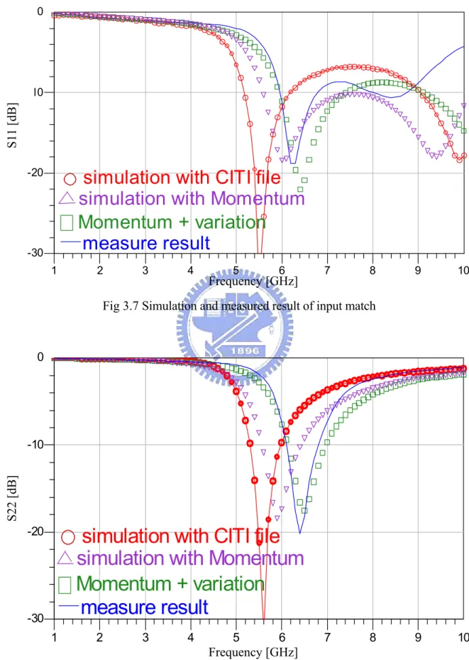
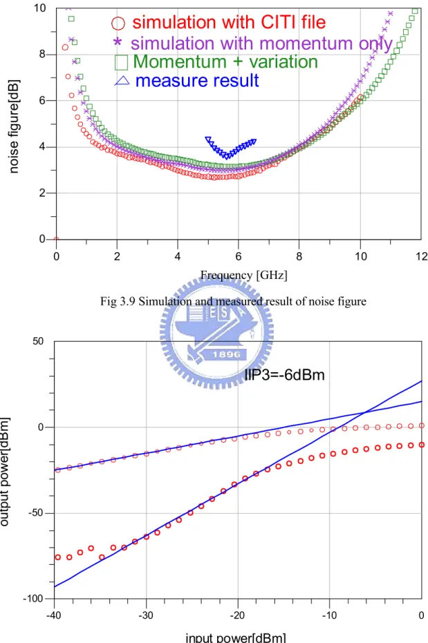
(43) simulation minus ten percent of inductance of every inductor for trouble shotting. After trouble shotting, the simulated curve agree well to the measured date. Thus, we attribute the drift to that the realistic inductance of the inductor is smaller than the inductor modeling. Fig 3.9 shows the minimum noise figure is 3.5dB at 5.8GHz. Also, Linearity analysis is conducted by the two-tone test. Measured at 6 GHz, the two-tone test results of the third-order inter-modulation distortion are plotted in Fig. 3.10. The IIP3 is -6dBm and the 1-dB compression point -15dBm. The total power of the LNA circuit dissipates 11mW with a power supply 1.8V. TABLE I summarizes the performance of the Darlington pair LNA and comparison with general inductive source degeneration topology simulated by TSMC 0.18um CMOS model.. 20. 40. 20. 10. -20 -10. simulation with CITI file simulation with Momentum Momentum + variation measure result. -20. -30 0. 1. 2. 3. 4. 5. 6. 7. 8. 9. -40. -60. -80. 10. Frequency [GHz] Fig 3.6 Simulation and measured result of power gain (S21) and isolation (S12). 30. S12[dB]. S21[dB]. 0 0.
(44) 0. S11 [dB]. -10. -20. simulation with CITI file simulation with Momentum Momentum + variation measure result. -30 1. 2. 3. 4. 5. 6. Frequency [GHz]. 7. 8. 9. 10. 9. 10. Fig 3.7 Simulation and measured result of input match. 0. S22 [dB]. -10. simulation with CITI file simulation with Momentum Momentum + variation measure result. -20. -30. 1. 2. 3. 4. 5. 6. 7. 8. Frequency [GHz] Fig 3.8 Simulation and measured result of output match 31.
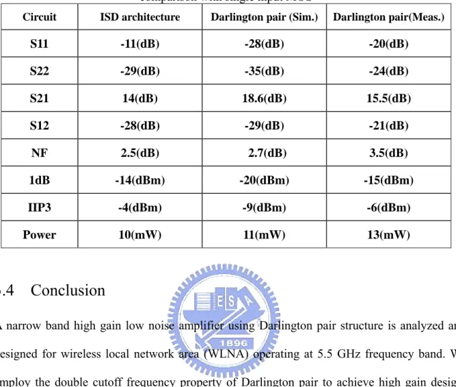
(45) 10. *. noise figure[dB]. 8. simulation with CITI file simulation with momentum only Momentum + variation measure result. 6. 4. 2. 0 0. 2. 4. 6. 8. 10. 12. Frequency [GHz] Fig 3.9 Simulation and measured result of noise figure 50. output power[dBm]. IIP3=-6dBm 0. -50. -100 -40. -30. -20. -10. input power[dBm] Fig 3.10 Measured result of two-tone test at 5 GHz. 32. 0.
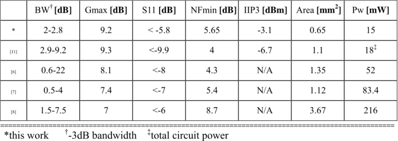
(46) TABLE I. Summary of simulation and measured result of Darlington pair LNA and comparison with single input MOS. Circuit. ISD architecture. Darlington pair (Sim.). Darlington pair(Meas.). S11. -11(dB). -28(dB). -20(dB). S22. -29(dB). -35(dB). -24(dB). S21. 14(dB). 18.6(dB). 15.5(dB). S12. -28(dB). -29(dB). -21(dB). NF. 2.5(dB). 2.7(dB). 3.5(dB). 1dB. -14(dBm). -20(dBm). -15(dBm). IIP3. -4(dBm). -9(dBm). -6(dBm). Power. 10(mW). 11(mW). 13(mW). 3.4 Conclusion A narrow band high gain low noise amplifier using Darlington pair structure is analyzed and designed for wireless local network area (WLNA) operating at 5.5 GHz frequency band. We employ the double cutoff frequency property of Darlington pair to achieve high gain design. Measured data show that the amplifier achieves maximum power gain (S21) of 15.5 dB, -10 dB input return loss (S11), and minimal noise figure of 3.5dB on the 5.8GHz frequency while consuming 13mW.. 33.
(47) CHAPTER 4 A 3 to 8GHz Ultra-Wideband CMOS LNA. 4.1 Introduction As the demand for broadband data communication increases, the ultra-wideband (UWB) system is an emerging wireless technology for transmitting high-speed digital data over a wide spectrum of frequency bands at a very low power level. The low noise amplifier (LNA) in the receiver path of the UWB system critically determines several system parameters. The amplifier must hold flat gain, minimum noise figure, broadband input impedance matching, and good linearity, over the entire frequency band. In recent years, distributed amplifiers (DAs) were widely used to realize broadband amplifier [6-8]. The architecture is generally large in size because of many on-chip inductors, and consumes a high power level owing to several stages cascaded to derive an adequate gain level. An interesting approach employs a band-pass filter as the broadband impedance matching network, and the technique of gain peaking to derive flat gain [11]. In doing so, an additional capacitor is required to be placed in parallel to the gate-source of the input device for the filter design, which results in lower cut-off frequency (ωt) and available gain. In this chapter, an LNA suitable for ultra-wideband system is designed in a standard 0.18um CMOS process. With the techniques of negative feedback and gain compensation, this LNA circuit achieves the broadband requirement in low power consumption.. 4.2 Principle of the circuit design 4.2.1 Ultra-Wideband LNA Circuit Topology. 34.
(48) The schematic of the LNA circuit is shown in Fig.4.1. The circuit includes three stages of the common-source input stage m1 for input trans-conductance, the common-gate inter-stage m2 for less Miller’s effect and better reverse isolation, and the common-source buffer stage m3 as the output buffer. The resistors Rf and Rf1 not only provide negative feedback but also self-biasing. Circuit performance can be analyzed by the small signal equivalent circuit as shown in Fig4.2. The shunt elements, Zfm, Rfm1 and Rfm2, represent the Miller’s effect for Rf and Rf1. Note that we neglect the Miller impedance produced by Rf at the drain node of m1 since the input impedance of the common-gate stage is typically low. The overlap capacitance Cgd is ignored without loss of generality. The DC block capacitor Cpass is also neglected. Detail analysis is described as in the following.. Fig.4.1 Schematic of Ultra Wide-band LNA. 35.
(49) Lg. Id1. Ld1. Is2. Cd1. Cgs2. Id2. vgs3. Cgs1 Zin. Zfm. vout. Cgs3. Zin1 Vgs1. Cd2 1/gm2. Rfm1. Ld2. gm2vgs2. Ro gm3vgs3. Rfm2//Rd. gm1Vgs1. Input stage (Gm). Ls. Inter stage (β). Buffer stage (Zm). Fig.4.2 Small signal analysis of ultra wide band LNA. 4.2.2 Broadband Input Matching The configuration of inductive source degeneration would only provide narrow-band impedance matching to 50Ω [3]. The main advantage of the inductive source degeneration matching is on the high input trans-conductance at resonant frequency of the matching network. The detailed analysis of the input trans-conductance is shown in the following section 4.2.3. To preserve the advantage, the technique of resistive negative feedback is therefore employed to extend the frequency band of the matching network [8]. Thus, the matching network of the LNA is the combination of resistive negative feedback and inductive source degeneration matching network. From small signal analysis in Fig.4.2, The input impedance can be derived as. Zin = Z fm || Zin1 ≈. Rf 1 − Av 0 ( s ). ⎛ ⎜ ⎝. || ⎜ s ( L. ⎞. 1 +L )+ +ω L ⎟ g s t s⎟ sC gs1 ⎠. (4-1). where Zfm is the miller impedance of the feedback resistor Rf and Av0(s) is the voltage gain from Vin to Vsg2. For the case at very low frequencies, Zin1 is close to an open-circuit due to the gate capacitance Cgs1, and the input impedance is 1+ R Zin ( ω ≈ 0 ) =. f. gm2. (4-2). g m1 + g m 2. a resistive level determined by the feedback resistor (Rf) as well as the trans-conductance of transistors m1 and m2. On the Smith chart as shown in Fig.4.6, we place the Zin(ω~0) at point 36.
(50) I, which is a resistive value higher than 50(Ω). For the case at the resonant frequency (ω01), Zin1 is a low resistive value (ωtLs) compared to Zfm, thus the total input impedance Zin is approximately equal to Zin1: Zin( ω = ω01) ≈ Z fm. g gm1 L s ≈ m1 L s Cgs1 Cgs1. (4-3). The Zin (ω=ω01) which is approximately a resistive value lower than 50(Ω) were placed around Point Ⅱ in Fig.4.6. Since these two levels Zin(0) and Zin(ω01) give the impedance range as the frequency sweeps, adjusting both levels near 50Ω shall ensure good S11 over the entire frequency band. Similarly output impedance matching is realized by the parallel connection of Rfm2 and Rd, as shown in Fig.4.2.. 4.2.3 Gain flatness technique Gain flatness is realized by gain compensation among the three stages. Under the condition of impedance match, available power gain shall be the same as the voltage gain. From the model in Fig.4.2, the overall voltage gain can be expressed as. Fig.4.3 Illustration of signal amplification. 37.
(51) Vout. Av =. =. Id1. *. *. Id1. Vin. Vin. I d2. Vout. = Gm * β * Zm. I d2. (4-5). where Gm is the trans-conductance of the input stage, β is the current gain of the inter-stage, and Zm is the transfer function of the buffer stage. Although the frequency response of each stage appears as narrow-band tuned, the composite response can achieve broadband gain flatness with appropriate design. An inter-stage matching inductor Ld1 is inserted in the cascoded configuration to enhance the gain level at high frequencies [12]. As illustrated in Fig.4.3, the frequency responses of the first two stages are tuned with peaking around 8-GHz, while that of the third stage around 3-GHz. As a result, the frequency response of the cascaded circuit yields to broadband gain flatness. The trans-conductance Gm of the input stage can be derived as. Gm =. Id1 = Vin. where. (ω. 2. gm1ω 01 ω s 2 + s 01 + ω 01 Q1. 01. =. 1 (L. + L )C g s gs1. (4-6). Q = 1 ω. 1 g L 01 m1 s. ). the response which is a second low pass filter reaches for a maximum at the resonant frequency (ω01). In this work the resonant frequency is set to be around the frequency of 8GHz, and the value of Q1 is chosen to broaden the bandwidth. The frequency response of the Gm is shown in Fig.4.3 (a). Note that, the larger the Q1, the higher the trans-conductance (Gm) in our operating frequency band. Under matching issue from above section mentioned in (4-3), the Ls is chosen lower than general inductive source degeneration narrow band LNA, which gives matching input impedance to 50(Ω) at resonant frequency. Thus, we can derive higher Q1 as well as Gm in the frequency band from 3 to 8 GHz. The inductor Ld1 is tuned to resonate with the drain capacitance (Cd1) of m1 and 38.
(52) gate-source capacitance (Cgs2) of m2. Together they are considered as a part of the inter-stage. The transfer function of current gain β is. β =. g m2 3 s C. 2 L C L +s g + s(C +C )+g gs2 d1 d1 m2 d1 d1 gs2 d1 m2 C. (4-7). With the inductor Ld1, the response at the frequency of 8-GHz is further boosted, as shown in Fig.4.3 (b). The trans-impedance Zm of the buffer stage is required to compensate for the roll-off generated by the overall trans-conductance of the first two stage, Gm*β. The transfer function of Zm is derived as. Zm =. where. Vout = i g2. 2. sω 02 * g m 3 * (R fm 2 R d R o ) ω 02 2 2 + ω 02 s +s Q2. (ω 02 =. 1 C t L d2. Q 2 = R fm1ω 02 C t. (4-8). C t = C gs3 + C d2 ). The inductor Ld2 is tuned to resonate with the gate-drain capacitance (Cgd2) and the gate-source capacitance (Cgs3) at the frequency of 3GHz. The response is shown in Fig.4.3(c). The cascaded circuit can achieve a flat voltage gain over the entire frequency band, as shown in Fig.4.3 (d).. 4.2.4 Design Considerations and Trade off The resistance of Rf shall be designed appropriately for impedance matching. The resistance, however, shall be large to minimize noise performance degradation. From simulation the value is chosen as 200Ω. High trans-conductance in the input stage yields to good noise performance. Since the 39.
(53) trans-conductance of the input stage appears as narrow-band tuned, noise performance of the designed circuit is better near the in-band high frequency of 8-GHz. In addition, tuning at higher frequency calls for a smaller gate inductance Lg. Consequently the parasitic resistance is smaller in practice, and the degradation to noise performance is minimized. Simulation shows the minimum noise figure is 4.5 dB around 8GHz, and the maximum value is 6 dB around 3-GHz. To meet the requirement of Zm, the value of the inductor Ld2 is chosen around 6 nH. The self resonant frequency of this inductor must be high above the frequency range for broadband operation. On the other hand, use of a low-Q inductor is acceptable as far as the broadband application is concerned. Thus, the metal width of 8um, narrower than the typically size in the design kit, is actually applied to this design to reduce parasitic capacitance and the occupied area. All of the inductors and interconnects are analyzed by the electromagnetic simulation tool of Agilent MOMENTUM. Circuit performance is analyzed together with the simulated S-parameters of the passives.. 4.3. Chip Implementation and Measured Result. 4.3.1 Microphotograph of Chip A microphotograph of the LNA circuit is shown in Fig.4.4. The circuit is fabricated in the TSMC 0.18um CMOS technology. The die area including bonding pads is 0.81 mm by 0.8 mm. As can be seen, the size of Ld2 is approximately the same as that of the inductor Lg (~1.2nH and metal width =15um).. 40.
數據
![Fig 3.6 Simulation and measured result of power gain (S21) and isolation (S12) Frequency [GHz]](https://thumb-ap.123doks.com/thumbv2/9libinfo/8471180.183549/43.892.111.768.546.996/fig-simulation-measured-result-power-gain-isolation-frequency.webp)
+6
相關文件
Have shown results in 1 , 2 & 3 D to demonstrate feasibility of method for inviscid compressible flow
In Section 3, the shift and scale argument from [2] is applied to show how each quantitative Landis theorem follows from the corresponding order-of-vanishing estimate.. A number
New topics in Wave 3 included positive education (2 principals). There were 2 principals reporting in Wave 3 that they had not participated in any professional development
Let us suppose that the source information is in the form of strings of length k, over the input alphabet I of size r and that the r-ary block code C consist of codewords of
1) Ensure that you have received a password from the Indicators Section. 2) Ensure that the system clock of the ESDA server is properly set up. 3) Ensure that the ESDA server
• A sequence of numbers between 1 and d results in a walk on the graph if given the starting node.. – E.g., (1, 3, 2, 2, 1, 3) from
首先,在前言對於為什麼要進行此項研究,動機為何?製程的選擇是基於
Even though the σ−modification term in the parameter tuning law and the stabilizing control term in the adaptive control law are omitted, we shall show that asymptotical stability
