國
立
交
通
大
學
電子工程學系 電子研究所碩士班
碩 士 論 文
原子層沉積三氧化二鋁介電層於砷化銦鎵金氧半電
容之電性與化性的研究
Study on Electrical and Chemical Characteristics of
Indium Gallium Arsenide
Metal-Oxide-Semiconductor Capacitors with
Atomic-Layer-Deposited Al
2O
3Gate Dielectric
研 究 生:鄒秉翰
指導教授:簡昭欣 教授
原子層沉積三氧化二鋁介電層於砷化銦鎵金氧半電
容之電性與化性的研究
Study on Electrical and Chemical Characteristics of
Indium Gallium Arsenide
Metal-Oxide-Semiconductor Capacitors with
Atomic-Layer-Deposited Al
2O
3Gate Dielectric
研 究 生:鄒秉翰 Student:Ping-Han Tsou
指導教授:簡昭欣 教授 Advisor:Dr. Chao-Hsin Chien
國 立 交 通 大 學
電 子 工 程 學 系 電 子 研 究 所 碩 士 班
碩 士 論 文
A Thesis
Submitted to Department of Electronics Engineering and Institute of Electronics College of Electrical and Computer Engineering
National Chiao Tung University In Partial Fulfillment of the Requirements
For the Degree of Master of Science In Electronics Engineering
April 2013
Hsinchu, Taiwan, Republic of China
I
原子層沉積三氧化二鋁介電層於砷化銦鎵金氧
半電容之電性與化性的研究
學生:鄒秉翰
指導教授:簡昭欣 教授
國立交通大學
電子工程學系 電子研究所碩士班
摘要
在此篇論文初,我們主要研究晶向(100)的砷化銦鎵通道層與三氧化二鋁(原 子層沉積,ALD)之間的界面。粗劣的界面和氧化層品質會導致高頻率分散、費 米能階釘札及高閘極漏電流。為了要改善界面與閘極氧化層間的品質,不同的熱 處理作用在電容上,例如:後金屬化退火(PMA)、氮氫混合氣體退火(FGA)、後沉積退火(PDA)。首先,我們先探討電容經過 PMA 的處理與 FGA 處理後的
差異。與 PMA 相比,在聚積區的頻率分散可被 FGA 有效地降低。另外,我們
利用電導法來萃取界面缺陷電荷密度(Dit);在能隙深處(midgap)的缺陷電荷經
過 FGA 後可被輕微地降低,例如:Dit (Et= 0.428 eV)在 FGA 後降低約 22.28%。
其後,電容在 FGA 下與不同 PDA 的效應也已探討。從量測的數據分析指出電容 在 PDA 溫度 500 度 120 秒及 FGA 下展現最差的電性。此外,越高的 PDA 溫度,
越高的 Dit存在於能隙深處。電性之所以劣化的原因,從 XPS 分析來看為較低的
II 的實驗中,晶向(100)砷化銦鎵的電性較優於晶向(111)A 砷化銦鎵的電性, 如較低的頻率分散和較低的 Dit。這個結果可能是因為相較於三氧化二鋁和晶向 (111)A 砷化銦鎵間的界面,有較高的 As2O3/As2O5於三氧化二鋁和晶向(100)砷化 銦鎵間的界面。 最後,根據TEM影像和EDX分析,自我對準鎳-砷化銦鎵合金之源極/汲極 之n型通道金氧半場效電晶體的失敗原因歸因於鎳-砷化銦鎵合金的未形成。其中, 最有可能阻礙鎳-砷化銦鎵合金形成的原因為原生氧化層存在於鎳與砷化銦鎵通 道層間。
III
Study on Electrical and Chemical
Characteristics of Indium Gallium Arsenide
Metal-Oxide-Semiconductor Capacitors with
Atomic-Layer-Deposited Al
2O
3Gate Dielectric
Student:Ping-Han Tsou Advisor:Dr. Chao-Hsin Chien
Department of Electronic Engineering & Institute of Electronics
National Chiao Tung University
ABSTRACT
In the beginning of the thesis, we have mainly studied the interface between (100)-oriented In0.53Ga0.47As channel layer and Al2O3 (atomic layer deposition, ALD).
Poor interface and oxide qualities may cause high frequency dispersion, Fermi level pinning, and high gate leakage current. In order to improve interface and gate oxide qualities, different thermal treatments are applied to the capacitors, such as post-metallization annealing (PMA), forming gas annealing (FGA), and post deposition annealing (PDA). Firstly, we study the difference between the capacitors treated with PMA and those treated with FAG. Compared to PMA, frequency dispersion in accumulation can be efficiently reduced by FGA. In addition, we utilize the conductance method to extract the interface state density (Dit). The midgap traps
IV
FGA. Subsequently, the effects of MOSCAPs under different PDA temperature with FGA have also been discussed. It is noted that MOSCAPs under PDA 500 oC for 120 s with FGA show the worst electrical characteristics. Furthermore, higher PDA temperature is, the higher Dit exists close to midgap. The reason for the degradation of
electrical characteristics may be lower ratio of As2O3 to As2O5 and the precipitation of
arsenide, which is shown in our XPS analysis. Next, in our experiment, the electrical characteristics of In0.53Ga0.47As (100) is better than In0.53Ga0.47As (111)A, such as
lower frequency dispersion and lower Dit. This consequence is possibly due to higher
amounts of As2O3/As2O5 at the Al2O3/In0.53Ga0.47As (100) interface, compared to
Al2O3/In0.53Ga0.47As (111)A interface.
Eventually, the failure of self-aligned Ni-InGaAs S/D In0.53Ga0.47As n-MOSFETs
is attributed to the non-formation of Ni-InGaAs according to the TEM image and EDX analysis.The possible reason that inhibits the formation of Ni-InGaAs may the existence of native oxides between Ni and In0.53Ga0.47As channel layer.
V
誌謝
自由自在的學生生涯終於要畫下最後的休止符了。兩年多的碩士生活,經歷 了不只是在課業上所遇到的困難,還有生活上許多大大小小的喜怒哀樂等。首先, 感謝我的指導老師-簡昭欣教授,提供挑戰的自由學習環境與實驗資源,讓我們 更可以知道一個成功的元件製程,是需要經過多少次的測試、嘗試、實驗和到最 後的量測分析。無數次的失敗與打擊、外在無預期的因素,真的是層層關卡、層 層磨練,不經意佩服前人在這領域上的貢獻,及克服瓶頸的心理素質。另外,老 師時常告訴我們做出來成品的特性,不一定是要最好的,但要有創新性,有其獨 特與眾不同的地方。同樣的道理,我想在各行各業或人生道路上都有其應用價值 與幫助。最後再次感謝老師如此耐心地等待我完成碩士學業,也非常珍惜這段研 究生的點點滴滴與經驗,永生難忘! 信淵學長,非常感謝您在最後的拔刀相助!這段時間裡的學習真的非常充實, 也讓我見識到您的廣博知識及驚人的 paper 海,問題每問必答;也謝謝學長能配 合我做實驗的時間,期待未來還可以一起歡樂籃球。政庭學長,您的製程手藝與 敏銳判斷真是讓我望洋興嘆!每次在製程遇到問題和經驗,都可以好好請教您一 番,也感謝您的指教提醒與製程機台的給力幫忙。哲偉學長,實驗室的歡樂籃板 王斑蛙,常常帶來意想不到的促咪,感謝您在製程與分析上的教導。您在實驗上 的認真拚勁和熱誠,我想這輩子再怎麼努力,也是望塵莫及。這精神我會好好運 用在其他領域上,也期待聽到您早日被交易(畢業)出去阿!家豪學長,感謝您 在一些問題的指點迷津和經驗分享,常常能感受到您的邏輯思考和處理問題的功 力,也恭喜您完成博士學業。偉大的 Acer 學長,非常欽佩您能學業生活兼顧, 也是我碩士生涯希望可以做到的。在無塵室聊天總是能得到一些不錯的想法和樂 趣,也感謝您的前期機台訓練和幫忙與打氣,讓我們做實驗的時候感受不到孤單! 整個新竹只有一個宏基!東昇學長,謝謝您的工作經驗分享與建議,讓我更珍惜VI 學生的好,也讓我對未來有更多的想法,非常欽佩您能在工作狀態下又能堅持學 業,也祝福您能在今年能同時拿到兩張證書!感謝昶智和韋志學長的指教和幫助, 尤其是製程 SOP 精神,難人可貴!在此也祝福碩博班學長們都能順利畢業和工作 事業順利,快快樂樂。 哲鎮、就舉哥,跟你們住在一起的三個月多,一起吃飯,一起互嗆,尤其是 即將離別的惡靈之夜,不亦樂乎!小林,從大學到研究所的夥伴,咱們的活計算 機,同為三重埔人的驕傲!從你們身上學習不少特質,也認識到更多的朋友,一 同努力的甘苦實驗人生,一同歡笑,難以忘懷!也祝你們在未來的道路上一切順 利,成功的話,請多多提拔小弟我!也感謝邦聖和主元的機台供應,讓你們做了 不少白工,真不好意思!小弟才疏學淺,實驗沒幫你們太多,請見諒!小龜和純 敏也希望你們實驗有所突破和進展,一切順利!碩一學弟們就不一一唱名了,希 望你們都能找到自己想走的路,熬過來就是你們的。 旅途上,陪伴我度過無數的喜怒哀樂、酸甜苦辣的朋友們:從小一起在三重 埔長大的六人幫、高中的 bro 們和皇家滑輪社的姐妹們、中山物理兄弟們、NPNT 的姐姐和辣媽們、師大心測的帥哥美女們、對岸的天大、東北、北大朋友們、曾 經一同出遊的朋友們......等。總之,沒有你們,就沒有今天的小弟我, 謝謝你們一路的支持與不斷的出現,也希望你們能幸福美滿。 最後特別感謝我的家人們,不論是在經濟上和精神上的支持,讓我到這年紀 還能享受無憂無慮的學生生活,謝謝你們讓我完成交大夢,也讓我有機會再去更 多地方,目睹山川水秀和友誼結交。或許未來不一定會繼續走同樣的路,但我想 某些道理應該也適用在其它條道路吧!自己的人生自己負責,趁年輕多去嘗試、 多出去看看與經歷、多吃苦、多拓展人脈,我想慢、難、苦之路或許可以體驗和 收獲更多吧! 9911514 下線,準備國軍 on-line! 鄒秉翰 於新竹交通大學 2013 年 3 月 15 日
VII
Contents
Abstract (Chinese) ... I Abstract (English) ... III Acknowledgement ... V Contents ... VII Figure Captions ... IX Table Captions ... XIV
Chapter 1 ... 1
1.1 General Background ... 1
1.2 Motivation ... 2
1.3 Organization of the Thesis ... 3
Reference (Chapter 1) ... 4
Chapter 2 ... 9
2.1 Introduction ... 9
2.2 Experimental Procedures ... 11
2.2.1 Al2O3/In0.53Ga0.47As (100) MOSCAPs Pretreated with Trimethylaluminium... ... 11
2.2.2 Al2O3/In0.53Ga0.47As (111)A MOSCAPs Pretreated with Trimethylaluminium ... 12
2.3 Electrical Characteristics of ALD-TMA/In0.53Ga0.47As (100) and Interfacial Chemistry ... 13
2.3.1 C-V Measurements of MOSCAPs w/ or w/o FGA ... 14
2.3.2 C-V and G-V Measurements of MOSCAPs w/ FGA or PMA ... 15
2.3.3 Electrical and Chemical Characteristics of MOSCAPs w/ FGA under Various PDA Conditions ... 18
VIII
2.4 Electrical Characteristics of ALD-TMA/In0.53Ga0.47As (111)A and Interfacial
Chemistry ... 20
2.5 Conductance Method ... 22
2.5.1 Comparison between FGA and PMA ... 25
2.5.2 MOSCAPs with FGA under Various PDA Conditions... 26
2.5.3 Comparison between the orientation of (100) and (111)A... 28
2.6 Summary ... 29 Reference (Chapter 2) ... 31 Chapter 3 ... 88 3.1 Introduction ... 88 3.2 Transistor Fabrication ... 89 3.3 Failure analysis ... 90 3.4 Summary ... 92 Reference (Chapter 3) ... 93 Chapter 4 ... 100 Vita ... 102
IX
Figure Captions
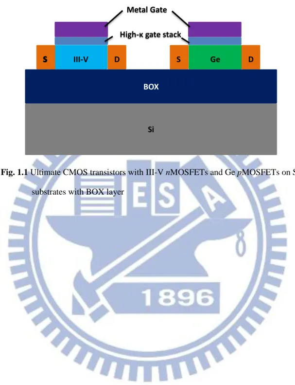
Fig. 1.1 Ultimate CMOS transistors with III-V nMOSFETs and Ge pMOSFETs on Si
substrates with BOX layer ... 7
Fig. 2.1 Process flow of (100)-oriented In0.53Ga0.47As channel MOSCAPs with different
thermal treatments ... 38
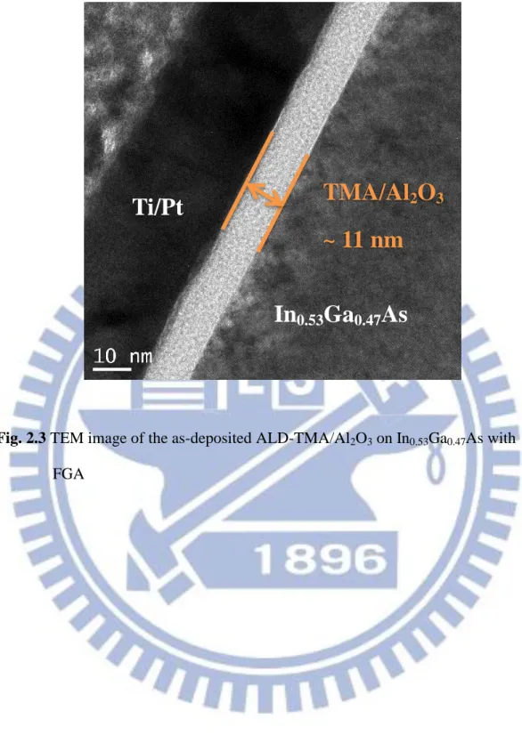
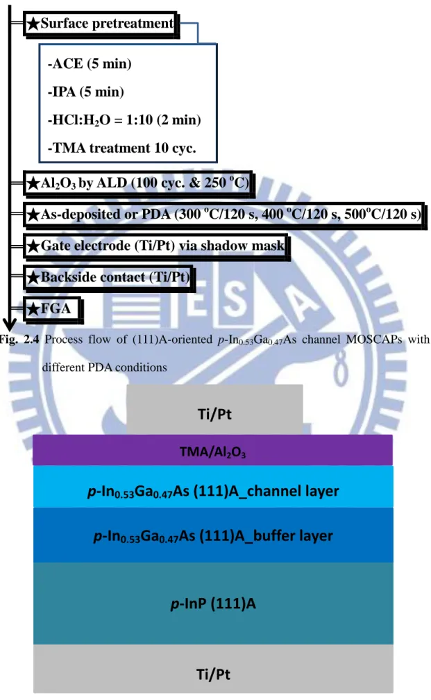
Fig. 2.2 MOSCAPs structure with ALD-TMA/Al2O3/In0.53Ga0.47As (100) ... 38 Fig. 2.3 TEM image of the as-deposited ALD-TMA/Al2O3 on In0.53Ga0.47As with FGA .. 39 Fig. 2.4 Process flow of (111)A-oriented p-In0.53Ga0.47As channel MOSCAPs with
different PDA conditions... 40
Fig. 2.5 MOSCAPs structure with ALD-TMA/Al2O3/In0.53Ga0.47As (111)A ... 40 Fig. 2.6 Frequency-dependent C-V characteristics (100 kHz to 100 Hz, 300K) for p-type
Pt/Ti/TMA+Al2O3/In0.53Ga0.47As (100) MOSCAPs (as-deposited) (a) w/o FGA
and (c) w/ FGA ... 41
Fig. 2.7 Frequency-dependent C-V characteristics (100 kHz to 100 Hz, 300K) for n-type
Pt/Ti/TMA+Al2O3/In0.53Ga0.47As (100) MOSCAPs (as-deposited) (b) w/o FGA
and (d) w/ FGA ... 42
Fig. 2.8 Multifrequency C-V curves (1 MHz to 100 Hz, 300K) for p-type
Pt/Ti/TMA+Al2O3/In0.53Ga0.47As (100) MOSCAPs (as-deposited) with (a)
FGA and (c) PMA ... 43
Fig. 2.9 Multifrequency C-V curves (1 MHz to 100 Hz, 300K) for n-type
Pt/Ti/TMA+Al2O3/In0.53Ga0.47As (100) MOSCAPs (as-deposited) with (b)
X
Fig. 2.10 Map of the normalized conductance, (G/ω)/Aq, as a function of gate bias VG
and frequency f measured at 300K for MOSCAPs with Al2O3 (as-deposited) on
p-type In0.53Ga0.47As (100) after (a) FGA and (c) PMA ... 45
Fig. 2.11 Map of the normalized conductance, (G/ω)/Aq, as a function of gate bias VG
and frequency f measured at 300K for MOSCAPs with Al2O3 (as-deposited) on
n-type In0.53Ga0.47As (100) after (b) FGA and (d) PMA ... 46
Fig. 2.12 Schematic diagram of tunneling between border traps in gate dielectric and
conduction band of semiconductor ... 47
Fig. 2.13 Band alignment between Al2O3 and common III-V compound semiconductors,
and position of charge-state transition levels for dangling bonds in the oxide ... 47
Fig. 2.14 Multifrequency C-V curves (1 MHz to 100 Hz, 300K) for p-type
Pt/Ti/TMA+Al2O3/In0.53Ga0.47As (100) MOSCAPs after post-metallization
FGA under different PDA conditions in N2 ambience for 120 s (a) 300 oC (b) 400 oC (c) 500 oC ... 49
Fig. 2.15 Multifrequency C-V curves (1 MHz to 100 Hz, 300K) for n-type
Pt/Ti/TMA+Al2O3/In0.53Ga0.47As (100) MOSCAPs after post-metallization
FGA under different PDA conditions in N2 ambience for 120 s (a) 300 oC (b)
400 oC (c) 500 oC ... 51
Fig. 2.16 Map of the normalized conductance, (G/ω)/Aq, as a function of gate bias VG
and frequency f measured at 300K for MOSCAPs with ALD-TMA/Al2O3 on
p-type In0.53Ga0.47As (100) after post-metallization FGA under different PDA
conditions in N2 ambience for 120 s (a) 300 oC (b) 400 oC (c) 500 oC ... 53 Fig. 2.17 Map of the normalized conductance, (G/ω)/Aq, as a function of gate bias VG
and frequency f measured at 300K for MOSCAPs with ALD-TMA/Al2O3 on
n-type In0.53Ga0.47As (100) after post-metallization FGA under different PDA
XI
Fig. 2.18 X-ray photoelectron spectroscopy of ALD-TMA (10 cycles)/Al2O3 (10 cycles)
on (100)-oriented In0.53Ga0.47As with post-metallization FGA under various
PDA conditions (a) Ga 2p3/2 (b) In 3d5/2 (c) As 2p3/2 ... 57
Fig. 2.19 Multifrequency C-V curves (1 MHz to 100 Hz, 300K) for p-type
Pt/Ti/TMA+Al2O3/In0.53Ga0.47As (111)A MOSCAPs after post-metallization
FGA under different PDA conditions in N2 ambience for 120 s (a) as-deposited (b) 300 oC (c) 400 oC (d) 500 oC ... 59
Fig. 2.20 Map of the normalized conductance, (G/ω)/Aq, as a function of gate bias VG
and frequency f measured at 300K for MOSCAPs with ALD-TMA/Al2O3 on
p-type In0.53Ga0.47As (111)A after post-metallization FGA under different PDA
conditions in N2 ambience for 120 s (a) as-deposited (b) 300 oC (c) 400 oC (d)
500 oC ... 61
Fig. 2.21 X-ray photoelectron spectroscopy of ALD-TMA (10 cycles)/Al2O3 (10 cycles)
on (111)A-oriented In0.53Ga0.47As with post-metallization FGA under various
PDA conditions (a) Ga 2p3/2 (b) In 3d5/2 (c) As 2p3/2 ... 63
Fig. 2.22 The band diagram of a n-type MOSCAP in depletion is shown in (a). (b)
Equivalent circuit of MOSCAP in depletion. (c) Measured circuit. ... 64
Fig. 2.23 (a) & (b) Charge trapping characteristics for In0.53Ga0.47As under different
temperature and corresponding measurement window with 100 Hz and 1 M Hz C-V measurement frequency ... 65
Fig. 2.24 Map of the normalized parallel conductance, (Gp/ω)/Aq, as a function of gate
bias VG and frequency f measured at 300K for MOSCAPs with Al2O3
(as-deposited) on p-type In0.53Ga0.47As (100) after (a) FGA and (b) PMA ... 66 Fig. 2.25 Map of the normalized parallel conductance, (Gp/ω)/Aq, as a function of gate
bias VG and frequency f measured at 300K for MOSCAPs with Al2O3
XII
Fig. 2.26 Parallel conductance curves of MOSCAPs with Al2O3 (as-deposited) on p-type
In0.53Ga0.47As (100) after (a) FGA and (b) PMA for VG= -1 to 1 volt. The
measurement is performed at 300K. ... 68
Fig. 2.27 Parallel conductance curves of MOSCAPs with Al2O3 (as-deposited) on n-type
In0.53Ga0.47As (100) after (a) FGA and (b) PMA for VG= 0.5 to -1.5 volts. The
measurement is performed at 300K. ... 69
Fig. 2.28 Al2O3/In0.53Ga0.47As (100) interface state distribution as determined from
conductance method, showing that MOSCAPs with (a) FGA and (b) PMA. The measurement is performed at 300K. ... 70
Fig. 2.29 Normalized parallel conductance, (Gp/ω)/Aq, as a function of gate bias VG and
frequency f measured at 300K for MOSCAPs with ALD-TMA/Al2O3 on
p-type In0.53Ga0.47As (100) after post-metallization FGA under different PDA
conditions in N2 ambience for 120 s (a) 300 oC (b) 400 oC (c) 500 oC. ... 72 Fig. 2.30 Normalized parallel conductance, (Gp/ω)/Aq, as a function of gate bias VG and
frequency f measured at 300K for MOSCAPs with ALD-TMA/Al2O3 on
n-type In0.53Ga0.47As (100) after post-metallization FGA under different PDA
conditions in N2 ambience for 120 s (a) 300 oC (b) 400 oC (c) 500 oC. ... 74 Fig. 2.31 Parallel conductance curves of MOSCAPs with Al2O3 on p-type In0.53Ga0.47As
(100) with post-metallization FGA and under different PDA conditions for VG= -1 to 1 volt (a) 300 oC (b) 400 oC (c) 500 oC. The measurement is
performed at 300K. ... 76
Fig. 2.32 Parallel conductance curves of MOSCAPs with Al2O3 on n-type In0.53Ga0.47As
(100) with post-metallization FGA and under different PDA conditions for VG= 0.5 to -1.5 volts.(a) 300 oC (b) 400 oC (c) 500 oC. The measurement is
XIII
Fig. 2.33 Al2O3/In0.53Ga0.47As (100) interface state distribution as determined from
conductance method, showing that MOSCAPs with post-metallization FGA and under different PDA conditions (a) 300 oC (b) 400 oC (c) 500 oC for 120s.
The measurement is performed at 300K. ... 80
Fig. 2.34 Normalized parallel conductance, (Gp/ω)/Aq, as a function of gate bias VG and frequency f measured at 300K for MOSCAPs with ALD-TMA/Al2O3 on p-type In0.53Ga0.47As (111)A after post-metallization FGA under different PDA conditions in N2 ambience for 120 s (a) as-deposited (b) 300 oC (c) 400 oC (d) 500 oC. ... 82
Fig. 2.35 Parallel conductance curves of MOSCAPs with Al2O3 on p-type In0.53Ga0.47As (111)A with post-metallization FGA and under different PDA conditions for VG= -1 to 1 volt. (a) as-deposited (b) 300 oC (c) 400 oC (d) 500 oC. ... 84
Fig. 2.36 Dit profiles of Al2O3/In0.53Ga0.47As (111)A MOSCAPs with FGA and under different PDA conditions. The measurement is performed at 300K. ... 85
Fig. 2.37 The comparison of Dit profiles between (100) and (111)A... 85
Fig. 3.1 Schematic cross-sectional image and technology requirements of future III-V MOSFETs ... 94
Fig. 3.2 Process flow and device structure of In0.53Ga0.47As channel n-MOSFET with self-aligned Ni-InGaAs source and drain ... 95
Fig. 3.3 I-V characteristics of metal/p-InGaAs diodes with different RTA conditions... 96
Fig. 3.4 Schottky barrier height (SBH) for electron of a variety of metals/In0.53Ga0.47As contacts from [2] ... 96
Fig. 3.5 Energy level for charge neutrality level (CNL) in InxGa1-xAs ... 97
Fig. 3.6 The cross-section TEM image of self-aligned metal S/D structure. . ... 97
XIV
Table Captions
Table 1.1 Material properties of bulk Si, Ge, GaAs, In0.53Ga0.47As, and InAs at 300K ... 8 Table 2.1 The overviews of frequency dispersion of ALD-TMA/Al2O3 (100)-oriented
In0.53Ga0.47As MOSCAPs ... 86 Table 2.2 The overviews of frequency dispersion of ALD-TMA/Al2O3 (111)A-oriented
p-In0.53Ga0.47As MOSCAPs at VG = -2 ... 86 Table 2.3 Ratio of the fitted area of the As-As and As- components and As2O3 to As2O5
from the As 2p3/2 spectra for the In0.53Ga0.47As (100) samples at different PDA
conditions ... 86
Table 2.4 Ratio of the fitted area of the As-As and As- components and As2O3 to As2O5
from the As 2p3/2 spectra for the In0.53Ga0.47As (111)A samples at different
PDA conditions ... 87
Table 2.5 The overviews of Dit values of ALD-TMA/Al2O3 (100)-oriented and
(111)A-oriented In0.53Ga0.47As under different thermal treatments... 87 Table 3.1 Etch selectivity of Ni over Ni-InGaAs in different etchants. [4] ... 99
1
Chapter 1
Introduction
1.1 General Background
As the scaling of Si-based metal-oxide-semiconductor field effect transistors (MOSFETs) is approaching the physical limit, development of high mobility channel material has been recognized as a potential solution to sustain performance improvements in the upcoming sub-10nm gate length era [1]. Particularly, III-V compound semiconductors are one of the most promising candidates for realizing high performance n-channel metal-insulator-semiconductor field effect transistors (MISFETs) [2,3] due to their high electron mobilities. In 1965, Becke and White reported the first GaAs MOSFET work, using SiO2 as the gate dielectrics with a large
amount of interface states [4]. It was obviously realized that SiO2 might not the right
gate dielectrics for III-V compound semiconductors. Therefore, a variety of dielectrics and techniques have been investigated in the following decades. In 1987, researchers at Bell Labs discovered that sulfur passivation on the surface of III-V semiconductors before dielectrics deposition can improve electrical characteristics [5,6]. The first inversion channel GaAs MOSFETs with MBE-grown Ga2O3 (Gd2O3) as a gate
dielectric were announced in 1996 from Bell Labs [7-9]. After that a series of device work were led by Hong and Ren, including InGaAs enhancement-mode (E-mode) MOSFETs [10] and GaAs complementary MOSFETs [11]. At the end of 2001, Ye and Wilk started to work on atomic-layer-deposition (ALD) high-κ Al2O3 and HfO2 on
2
III-V materials [12]. Detailed interface studies were carried out to demonstrate the unpinning of the Fermi level in III-V semiconductors using ALD high-κ dielectrics [13-15]. In particular, In-rich InGaAs is identified as the potential III-V material for future technology node with higher effective mobility and manageable band gap for low drain voltage.
In the future generations, CMOS fabricated by integrating III-V nMOSFETs and Ge pMOSFETs, respectively, because of their high electron and hole mobilities, shown in Table 1.1, on the same Si platform, shown in Fig. 1.1, can be one of the ultimate CMOS structure [16].
1.2 Motivation
One of the major problems enabling widespread use of III-V compound semiconductors to fabricate MOSFETs is lack of a high quality, natural insulator for III-V substrates like that available for the SiO2/Si material system [17]. In order to
realize MOSFETs with III-V channels, suitable gate dielectrics must form a stable interface within the thermal budget of the transistor fabrication process, possess a high dielectric constant and sufficient band offsets with semiconductor conduction band to allow for scaling and low gate leakage, and have a low interface states density (Dit). Especially, engineering the interface between the III-V channel material and
gate oxide is extremely challenging.
The other challenge to achieve high performance III-V MOSFETs is the reduction of source and drain (S/D) series resistance (RS/D), which includes
metal-semiconductor contact resistance [18]. Therefore, we have to find the appropriate techniques and conditions to engineer S/D region.
3
For MOSFET surface channels beyond the 16 nm node, the candidate III-V material InxGa1-xAs alloys which have a band gap of (0.36≦Eg≦1.42 eV) and Eg≧
14kT are potentially suitable for many applications with power supply operating voltages≦ 0.5 V envisioned for short gate lengths (Lg≦ 20 nm) [19]. In particular,
alloys with an In content greater than 50% are commonly used as a channel material due to their high electron mobility relative to Si. Here, we use In0.53Ga0.47As as a
channel layer which is epitaxial growth on InP substrates to do our studies.
1.3 Organization of the Thesis
In Chapter 1, we gave a brief overview on the history and main obstacles in realizing III-V MOSFET. Current status of CMOS research was also described.
In Chapter 2, in order to study the interface between In0.53Ga0.47As and Al2O3,
conductance method was applied to admittance measurement from metal oxide semiconductor capacitors (MOSCAPs). The influence of post-metallization N2
annealing (PMA), post-metallization forming gas annealing (FGA), and post deposition annealing (PDA) were demonstrated. In addition, the difference in electrical characteristics between the orientation of (100) and (111)A was also studied. In Chapter 3 and Chapter 4, we tried to fabricate In0.53Ga0.47As channel
nMOSFETs with self-aligned Ni-InGaAs source and drain. Although the devices could not work, we found the possible reasons for the failure of our n-MOSFETs. Eventually, we made the conclusion as mentioned above and gave some suggestions for future works.
4
Reference (Chapter 1)
[1] S. Takagi, T. Irisawa, T. Tezuka, T. Numata, S. Nakaharai, N. Hirashita, Y. Moriyama, K. Usuda, E. Toyoda, S. Dissanayake, M. Shichijo, R. Nakane, S. Sugahara, M. Takenaka, N. Sugiyama, “Carrier-Transport-Enhanced Channel CMOS for Improved Power Consumption and Performance,” IEEE Trans. Electron Devices, vol. 55, p. 21, 2008.
[2] S.H. Kim, M. Yokoyama, N. Taoka, R. Iida, S. Lee, R. Nakane, Y. Urabe, N. Miyata,T. Yasuda, H. Yamada, N. Fukuhara, M. Hata, M. Takenaka, S. Takagi, “Self-aligned metal Source/Drain InxGa1-xAs n-MOSFETs using Ni-InGaAs
alloy, ” Tech. Dig. Int. Electron Devices Meet., p. 596, 2010.
[3] H.C. Lin, W.E. Wang, G. Brammertz, M. Meuris, M. Heyns, “Electrical study of sulfur passivated In0.53Ga0.47As MOS capacitor and transistor with ALD Al2O3 as
gate insulator,” Microelectron. Eng., vol.86, p.1554, 2009.
[4] H. W. Becke, R. Hall, and J. P. White, “Gallium arsenide MOS transistor,” Solid-State Electronics, vol. 8, p. 813, 1965.
[5] B. J. Skromme, C. J. Sandroff, E. Yablonovitch, and T. Gmitter, “Effects of passivating ionic films on the photoluminescence properties of gaas,” Applied Physics Letters, vol. 51, p. 2022, 1987.
[6] E. Yablonovitch, C. J. Sandroff, R. Bhat, and T. Gmitter, “Nearly ideal electronic properties of sulfide coated GaAs surfaces,” Applied Physics Letters, vol. 51, p. 439, 1987.
[7] M. Passlack, M. Hong, and J. P. Mannaerts, “Quasistatic and high frequency capacitance–voltage characterization of Ga2O3–GaAs structures fabricated by in
situ molecular beam epitaxy,” Applied Physics Letters, vol. 68, p. 1099, 1996. [8] M. Passlack, M. Hong, J. P. Mannaerts, R. L. Opila, S. N. G. Chu, N. Moriya, F.
5
Ren, and J. R. Kwo, “Low Dit thermodynamically stable Ga O3-GaAs in-
terfaces: fabrication, characterization, and modeling,” IEEE Transactions on Electron Devices, p. 214, 1997.
[9] M. Hong, J. Kwo, A. R. Kortan, J. P. Mannaerts, and A. M. Sergent, “Epitaxial Cubic Gadolinium Oxide as a Dielectric for Gallium Arsenide Passivation,” Science, vol. 283, p. 1897, 1999.
[10] F. Ren, J. M. Kuo, M. Hong, W. S. Hobson, J. R. Lothian, J. Lin, H. S. Tsai, J. P. Mannaerts, J. Kwo, S. N. G. Chu, Y. K. Chen, and A. Y. Cho, “Ga2O3(Gd2O3)/InGaAs Enhancement-Mode n-Channel MOSFET’s,” IEEE
Electron Device Lett., vol. 19, p. 309, 1998.
[11] M. Hong, J. N. Baillargeon, J. Kwo, J. P. Mannaerts, and A. Y. Cho, “First demonstration of GaAs CMOS,” Compound Semiconductors, 2000 IEEE
International Symposium on, p. 345, 2000.
[12] P. D. Ye, G. D. Wilk, B. Yang, J. Kwo, H.-J. L. Gossmann, M. Hong, K. K. Ng, and J. Bude, “ Depletion-mode InGaAs metal-oxide-semiconductor field-effect transistor with oxide gate dielectric grown by atomic-layer deposition,” Appl. Phys. Lett., vol. 84, p. 434, 2004.
[13] Y. Xuan, H. C. Lin, P. D. Ye, and G. D. Wilk, “Capacitance-voltage studies on enhancement-mode InGaAs metal-oxide-semiconductor field-effect transistor using atomic-layer-deposited Al2O3 gate dielectric,” Applied Physics Letters, vol. 88, p. 263518, 2006.
[14] Y. Xuan, H. Lin, and P. D. Ye, “Simplified surface preparation for GaAs pas- sivation using atomic-layer-deposited high-k dielectrics,” IEEE Transactions on Electron Devices, vol. 54, p. 1811, Aug 2007.
[15] Y. Xuan, H. Lin, and P. Ye, “Capacitance-voltage characterization of atomic- layer-deposited Al2O3/InGaAs and Al2O3/GaAs Metal-Oxide-Semiconductor
6
structures,” ECS Transactions, vol. 3, p. 59, 2006.
[16] M. Yokoyama, S. H. Kim, R. Zhang, N. Taoka1, Y. Urabe, T. Maeda, H. Takagi, T. Yasuda, H. Yamada, O. Ichikawa, N. Fukuhara, M. Hata, M. Sugiyama, Y. Nakano, M. Takenaka, and S. Takagi, “CMOS integration of InGaAs nMOSFETs and Ge pMOSFETs with self-align Ni-based metal S/D using direct wafer bonding,” IEEE Symposium on VLSI Technology, p. 60, 2011.
[17] G. D. Wilk, R. M. Wallace, and J. M. Anthony, “High-κ gate dielectrics: Current status and materials properties considerations,” J. Appl. Phys., vol. 89, p. 5243, 2001.
[18] A. Dimoulas, A. Toriumi, and S. E. Mohney, “Source and Drain Contacts for Germanium and III-V FETs for Digital Logic,” MRS Bull., vol. 34, p. 522, 2009. [19] C.L. Hinkle, E.M. Vogel, P.D. Ye, R.M. Wallace, “Interfacial chemistry of
oxides InxGa(1-x)As and implications for MOSFET applications,” Current
7
Fig. 1.1 Ultimate CMOS transistors with III-V nMOSFETs and Ge pMOSFETs on Si
substrates with BOX layer
Si
BOX
III-V D S Ge D High-κ gate stack
8 Si Ge GaAs In0.53Ga0.47As InAs Lattice constant (Å ) 5.431 5.646 5.653 5.869 6.058 Band gap (eV) 1.12 0.66 1.42 0.74 0.36 Permittivity 11.8 16 12 13.9 14.8 Intrinsic carrier conc. (cm-3) 9.6×10⁹ 2.4×10¹³ 2.2×10⁶ 7.7×10¹¹ 1×10¹⁵ Effective conduction band density of states (cm-3) 2.8×10¹⁹ 1.04×10¹⁹ 4×10¹⁷ 2.2×10¹⁷ 8.7×10¹⁶ Effective valence band density of states (cm-3) 1.04×10¹⁹ 6×10¹⁸ 9.7×10¹⁸ 7.8×10¹⁸ 6.6×10¹⁸ Electron mob. (cm2/Vs) 1600 3900 9200 12000 40000 Electron effective mass (/m0) mt: 0.19 ml: 0.916 mt: 0.082 ml: 1.467 0.067 0.043 0.023 Hole mob. (cm2/Vs) 430 1900 400 300 500 Hole effective mass (/m0) mHH: 0.49 mLH: 0.16 mHH: 0.28 mLH: 0.044 mHH: 0.45 mLH: 0.082 mHH: 0.45 mLH: 0.052 mHH: 0.57 mLH: 0.35
9
Chapter 2
Interface Studies of ALD-Al
2O
3/In
0.53Ga
0.47As
MOSCAPs with Different Annealing Conditions
and Orientations
2.1 Introduction
Recently, surface-channel In0.53Ga0.47As nMOSFETs have drawn much attention
as dimensional scaling of Si technology is progressively approaching the limits [1-4]. A longstanding problem for developing of these devices is the presence of interfacial defects that can cause Fermi level pinning or inefficient Fermi level response. Vacancies, antisite defects, or incomplete dimerization of the III-V surface can cause unsaturated bonds and form electrically active traps that may appear even before high-κ dielectric growth or are generated during the deposition [5]. On the other hand, the measured interface state densities are also deeply affected by the indium concentration. While indium content increases, the amount of air-grown Ga2O3
decreases probably due to the increased size of In atom reducing the available space for oxygen to bond to the interfacial gallium atoms [6]. High interface trap states would inhibit control over the charge carriers in the channel and the realization of MOSFETs with good performance. Therefore, the most important thing is to reduce Dit. Various passivation techniques and surface pre- or post-treatments [7-15] have
been considerably researched in the last several decades. Moreover, traps present in the bulk of a high-κ oxide layer may also have a great impact on the performance
10
owing to their potential to increase gate leakage current, scattering carriers in the channel, and threshold voltage shift of the device [16]. In addition, the prospects of III-V devices are brightening with the introduction of ALD for high-κ gate dielectric. Its precise thickness controllability is attributed to its surface-saturation controlled, layer by layer deposition kinetics [17]. Films deposited by ALD are conformal, pin-hole free, which normally can be further improved by thermal annealing. It is also noted that “self-cleaning” interfacial oxide reaction has been observed on III-V compound semiconductors such as GaAs [18-19], InGaAs [20].
Al2O3 is the most commonly used as a gate dielectric for III-V semiconductors
due to its less Fermi level pinning and thermal stability than HfO2. Furthermore,
trimethylaluminium (Al(CH3)3, “TMA”) is generally used as a metal precursor, which
is known to have more effective self-cleaning capability for removing native oxides on III-V surface than tetrakis(ethylmethylamino)hafnium (TEMA-Hf) used for the HfO2 deposition [21]. Here, we focus our study on the interface between
In0.53Ga0.47As and Al2O3. For the sake of further improving oxide quality and its
interface, several methods of thermal annealing have been applied to gate dielectric such as PDA, PMA and post-metallization FGA. Surface orientation of III-V channel is also an important parameter in controlling MIS properties. (111)A-oriented In0.53Ga0.47As has been investigated in different PDA conditions with FGA and is
compared with (100)-oriented In0.53Ga0.47As. Capacitance-Voltage (C-V)
measurements are traditionally utilized to characterize MOS devices and materials; besides, we use conductance method to extract interface states, which can be determined directly from the experiment [22]. In addition to studies on electrical characteristics, some chemical characteristics have been discussed.
11
2.2 Experimental Procedures
2.2.1 Al
2O
3/In
0.53Ga
0.47As (100) MOSCAPs Pretreated with
Trimethylaluminium
P-type (Zn-doped, 4×1018 cm-3) InP (100) wafers were used as the starting substrates. P-type (Zn-doped, 1×1017 cm-3) In0.53Ga0.47As (100) of 500 nm thick was
grown as a buffer layer, followed by a 300-nm p-type In0.53Ga0.47As (100) channel
layer (Zn-doped, 1.23×1016 cm-3). Similarly, the n-type (100)-oriented In0.53Ga0.47As
was grown on an In0.53Ga0.47As buffer layer on InP wafers. Because of air exposure,
all samples had initial native oxides on the In0.53Ga0.47As surface. To remove these
native oxides, suitable surface pretreatment must be carried out prior to gate dielectric deposition. In0.53Ga0.47As surfaces were initially rinsed for 5 minutes each in acetone
(ACE), isopropanol (IPA), followed by the dilute HCl solution (HCl:H2O = 1:10) for
2 minutes. Then the samples were transferred to ALD chamber as soon as possible. TMA treatment was performed for 10 cycles with a period of 0.06 s for a TMA pulse and 10 s for a N2 pulse at 250 oC before the subsequent Al2O3 deposition [23]. The
TMA-treated In0.53Ga0.47As surfaces were then in-situ coated with ALD-Al2O3 films
for 100 cycles, using alternating pulsed of TMA and H2O precursors at 250 oC and N2
as a purging gas to carry redundant reactants away. After that, the samples underwent PDA in N2 ambience with different annealing conditions, for instance, As-deposited,
and 300 oC, 400 oC, and 500 oC for 120 s. Circular MOSCAPs formation was done by sputter deposition of 50 Å of Ti and 500 Å of Pt through a shadow mask. The area of gate electrode examined by optical microscopy was 4×10⁻⁴ cm2. Backside ohmic contacts were formed by evaporation. Finally, some of the samples (no PDA) were completed by post-metallization annealing (PMA) in a N2 flow at 300 oC for 30 min,
12
and the others were carried out by forming gas annealing (FGA), which consists of a continuous flow of 5% H2/95% N2 ambience at 300 oC for 30 min.
The process flow and MOSCAPs structure are shown in Fig. 2.1 and Fig. 2.2. The cross-sectional TEM image of the as-deposited Al2O3 on In0.53Ga0.47As epitaxial
layers with TMA treatment (10 cycles) and FGA is shown in Fig. 2.3.
2.2.2 Al
2O
3/In
0.53Ga
0.47As (111)A MOSCAPs Pretreated with
Trimethylaluminium
P-type (Zn-doped) InP (111)A wafers were used as the starting wafers. P-type (Zn-doped) In0.53Ga0.47As (111)A of 500 nm thick was grown as a buffer layer,
followed by a 300-nm p-type In0.53Ga0.47As (111)A channel layer (Zn-doped,
3.43×1017 cm-3). Due to air exposure, all samples had initial native oxides on the In0.53Ga0.47As surface. To remove these native oxides, appropriate surface
pretreatment must be carried out prior to gate dielectric deposition. In0.53Ga0.47As
surfaces were initially rinsed for 5 minutes each in acetone (ACE), isopropanol (IPA), followed by the dilute HCl solution (HCl:H2O = 1:10) for 2 minutes. Then the
samples were transferred to ALD chamber as soon as possible. TMA treatment was performed for 10 cycles with a period of 0.06 s for a TMA pulse and 10 s for a N2
pulse at 250 oC before the subsequent Al2O3 deposition [23]. The TMA-treated
In0.53Ga0.47As surfaces were then in-situ coated with ALD-Al2O3 films for 100 cycles,
using alternating pulsed of TMA and H2O precursors at 250 oC and N2 as a purging
gas to carry redundant reactants away. After that, the samples underwent PDA in N2
ambience with different annealing conditions, for example, As-deposited, and 300 oC, 400 oC, and 500 oC for 120 s. Circular MOSCAPs formation was done by sputter
13
deposition of 50 Å of Ti and 500 Å of Pt through a shadow mask. The area of gate electrode examined by optical microscopy was 4×10⁻⁴ cm2. Backside ohmic contacts were formed by evaporation of Ti/Pt (50/500 Å ). Finally, all the samples were finished by forming gas annealing (FGA), which consists of a continuous flow of 5% H2/95% N2 ambience at 300 oC for 30 min.
The process flow and MOSCAPs structure are shown in Fig. 2.4 and Fig. 2.5.
2.3 Electrical Characteristics of ALD-TMA/In
0.53Ga
0.47As
(100) and Interfacial Chemistry
It has been taken a long time to develop MOS devices with various oxides on III-V compound semiconductors. The electrical characteristics of these MOSCAPs is closely related to processing conditions such as wafer preparation, passivation technique, dielectric deposition technique, PDA, PMA, FGA, etc. In this section, the electrical behaviors of Al2O3 on In0.53Ga0.47As with respect to interfacial chemistry
had been demonstrated. Capacitance-Voltage (C-V) and conductance-voltage (G-V) measurements were measured by HP4284A LCR meter at the temperature of 300K. Nevertheless, application of the technique to III-V systems requires considerable care, as described extensively by Passlack [24].
We quantitatively define frequency dispersion ratio ΔC. The equations ofΔC are as follows:
ΔC(@VG = -2 V)≡{[C(@1kHz) - C(@100kHz)]/C(@1kHz)}×100% p-type, (2.1)
ΔC(@VG = 2 V)≡{[C(@1kHz) - C(@100kHz)]/C(@1kHz)}×100% n-type, (2.2)
where ΔC is the frequency dispersion of capacitance measured in 1 kHz and 100 kHz at VG = 2 or VG = -2 volt. The overviews of frequency dispersion of the samples are
14 shown in Table 2.1.
2.3.1 C-V Measurements of MOSCAPs w/ or w/o FGA
The CV responses at room temperature (300K) with ac signal frequencies from 100 kHz to 100 Hz for the p-type and n-type Pt/Ti/Al2O3 (As-deposited)/In0.53Ga0.47As
MOSCAPs with or without FGA are shown in Fig. 2.6 (a) (c) and Fig. 2.7 (b) (d), respectively. It is noted that the C-V curves for p-type and n-type MOSCAPs are remarkably improved by FGA. The Table 2.1 shows that the frequency dispersion of
p-type MOSCAPs without FGA is 64.39%. After FGA, the frequency dispersion at VG
= -2 V dramatically reduces to 8.96%. Moreover, the stretch-out of C-V curves has also been improving after FGA. Correspondingly, the frequency dispersion and stretch-out of C-V curves for n-type MOSCAPs received FGA become well. In general, the stretch-out and frequency dispersion of the C-V curves are mainly caused by the existence of interface states. The higher the Dit, the larger the frequency
dispersion of the C-V curves and stretch-out. Therefore, we infer that the interface between gate dielectric and substrate might be restored by FGA, which is well known for passivating Pb-like defects in SiO2/Si and high-κ/SiOx/Si systems [25, 26]. Then,
we adjust the process flow, doing FGA subsequent to gate oxide deposition, to confirm whether FGA can reduce interface defects. However, we found that there is no marked difference in C-V curves between MOSCAPs without FGA and MOSCAPs with FGA subsequent to gate oxide deposition (not shown). FGA must be done after the deposition of gate metal probably for repairing the damage caused by sputter or improving the interface between gate dielectric and gate electrode.
15
2.3.2 C-V and G-V Measurements of MOSCAPs w/ FGA or
PMA
Fig. 2.8 (a) (c) and Fig. 2.9 (b) (d) show multifrequency C-V curves of
MOSCAPs with a thick (~11 nm) Al2O3 film on p- and n-type TMA treated
(100)-oriented In0.53Ga0.47As with FGA or with PMA, respectively, measured at 300K.
For the p-type, both two samples never reach strong accumulation, which indicates a high Dit close to the valence band edge. The frequency dispersion of MOSCAPs with
PMA is 12.34% larger than MOSCAPs with FGA, but much smaller than MOSCAPs without any post-metallization thermal annealing, shown in Table 2.1. A hump is seen at positive bias in both two samples, which may indicate the response of Dit. For the
n-type MOSCAPs, accumulation is achieved at positive gate bias. The frequency dispersion of MOSCAPs with PMA is 8.08% larger than MOSCAPs with FGA, also shown in Table 2.1. At negative gate voltages the total capacitance changes with gate bias and frequency, which may also indicate the response of interface states.
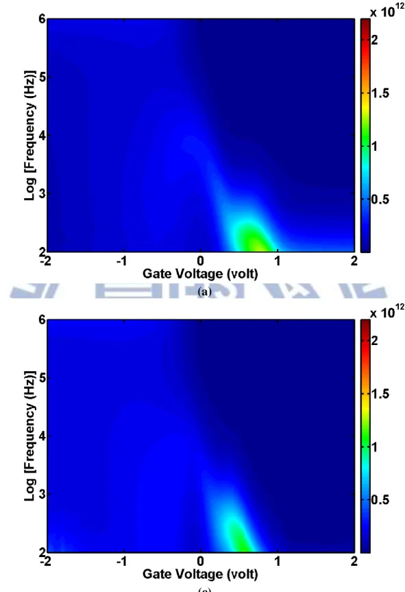
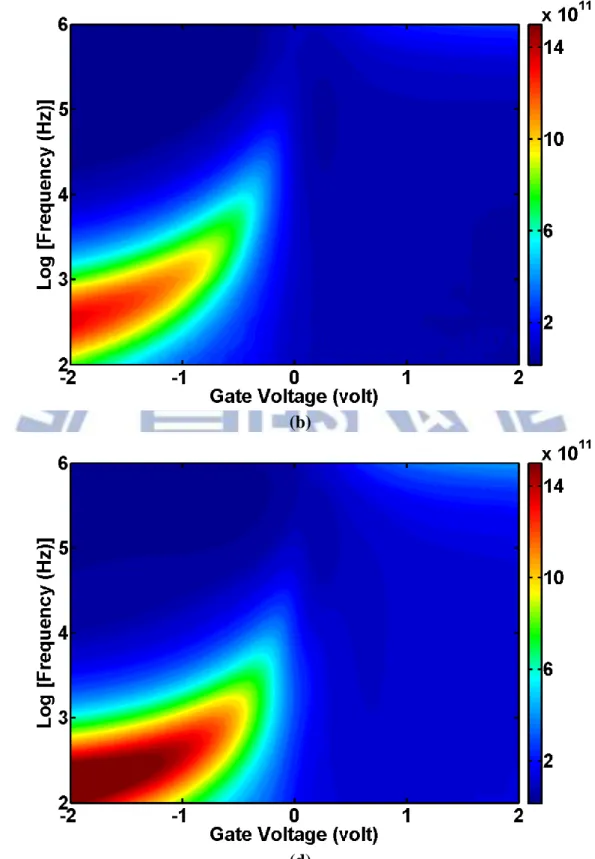
Fig. 2.10 (a) (c) and Fig. 2.11 (b) (d) show conductance maps of
Al2O3/TMA-treated In0.53Ga0.47As MOSCAPs with FGA or with PMA, on both p- and
n-type (100)-oriented In0.53Ga0.47As, respectively, at temperature 300 K. These maps
show the magnitude of normalized conductance (G/ω)/Aq as a function of ac frequency f and the gate voltage VG. For the p-type MOSCAPs, both two plots show
that a distinct signal exists at the gate voltage between 0 and 1 volt and at frequency between 100 Hz and 10 kHz. We speculate that this energy loss is caused by interface states due to its gate-voltage dependent and frequency-dependent conductance. For the n-type MOSCAPs, there is a conspicuous variation in color appearing at the negative gate voltage in both two graphs, which implies the dramatic energy loss.
16
Similarly, the G-V response to this energy loss is made by interface states owing to its gate-voltage dependent and frequency-dependent conductance. Additionally, the color variation at negative gate bias in Fig. 2.11 (b) is less dramatic than in Fig. 2.11 (d).
The frequency dispersion of the accumulation capacitance can be attributed to tunneling of carriers between the substrate and defect states in the ALD-Al2O3
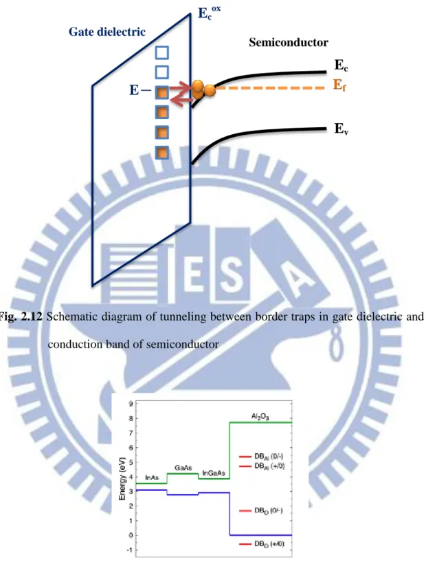
dielectric. The term “border traps” is referred to near-interfacial oxide traps that can exchange charge with substrate or gate, respectively [27]. While filling and emptying of interface states is a thermally activated process, tunneling of charges into border traps depends only on the measurement frequency and the distance of the defect states from the oxide/semiconductor interface. Some related studies have reported that the dispersion in the accumulation capacitance of such MOSCAPs is consistent with a tunneling mechanism for charge trapping, insensitive to temperature [28, 29]. Border traps that are close to conduction band edge of semiconductor contribute most effectively to the dispersion in accumulation, for n-type channel. Fig. 2.12 shows schematically the tunneling process between border traps and conduction band in an n-doped MOSCAP operated in accumulation. Our results are generally consistent with previous reports of hydrogen passivation of Al2O3/In0.53Ga0.47As, mainly passivating
border traps in the Al2O3 layer [30]. Since interface states nearly respond immediately
in deep accumulation, the decreased dispersion in accumulation observed in Fig. 2.8
(a) and Fig. 2.9 (c) may result exclusively from passivation of border traps.
Nonetheless, the response of interface states observed at VG=0~ -2 volts still exists
but less dramatic after FGA, shown in Fig. 2.11 (b), and also the evidence of interface states observed at VG=0~ 1 volt for p-type MOSCAPs, shown in Fig. 2.10 (a), does
not disappear after FGA. Therefore, we suppose that hydrogen is unable to completely reduce all interface states. Their binding energies are 2.52 eV for In-H, < 2.84 eV for Ga-H, and 2.84 eV for As-H [31]. Other researches consider that annealing in
17
hydrogen can remove most of the fixed oxide charge and interface states [32-34]. The presence of positive bulk fixed charge and negative interfacial fixed charge is identified as oxygen and aluminum dangling bonds (DBs), respectively. Fig. 2.13 shows the band alignment between Al2O3 and relevant semiconductors, and position
of charge-state transition levels for dangling bonds in the oxide from the reference [32]. After FGA, O DBs and Al DBs are neutralized by hydrogen, which the resulting binding energies are 1.3 eV for O-H and 1.4 eV for Al-H, respectively. However, some groups consider that the previously reports of FGA cannot be solely attributed to hydrogen passivation [35]. Hydrogen passivation of dangling bonds and border traps is responsible for improving the interfacial properties, while the thermal budget is responsible for minimizing the fixed charge. According to their opinions on the thermal effects of annealing, the presence of sufficient thermal energy can reconstruct the bonds to fill vacancies and to passivate dangling bond throughout the oxide. Another possibility is that PMA may provide enough thermal energy to break the O-H hydroxyl groups existing as a byproduct during the deposition of Al2O3. Hence, free
hydrogen dissociated from these O-H groups can also passivate dangling bonds, but the amount of hydrogen available would be limited by the presence of O-H bonds in the film.
In summary, FGA was found to suppress frequency dispersion in accumulation, which suggests that hydrogen could be a promising candidate as the method for passivation of border traps. In addition, it can also reduce some, but not all, interface states. Hydrogen annealing of these devices at 300 oC for 30 min has demonstrated better C-V and G-V characteristics, and we’ll further discuss the impact of PDA on the electrical characteristics of these MOSCAPs in the next section.
18
2.3.3 Electrical and Chemical Characteristics of MOSCAPs
w/ FGA under Various PDA Conditions
Fig. 2.8 (a), Fig. 2.14 (a) (b) (c) and Fig. 2.9 (b), Fig. 2.15 (a) (b) (c) show
multifrequency C-V curves of MOSCAPs with a Al2O3 film on p- and n-type TMA
treated (100)-oriented In0.53Ga0.47As after post-metallization FGA under different PDA
conditions, respectively, measured at 300K. For p-type, the MOSCAPs with PDA at 500 oC for 120 s exhibit the worst electrical characteristics. Although the capacitance value at VG= -2 volts of MOSCAPs with PDA 500 oC for 120 s is the largest, the
frequency dispersion of the samples with PDA 500 oC for 120 s severely degrades not only near accumulation (ΔC (@VG = -2 V) =16.91%) but also in depletion. It is noted
that the response of interface traps at VG= 0 to VG= 1 volt is severely getting large as
the temperature of PDA increases; therefore, for our In0.53Ga0.47As substrate, the
limited temperature of post deposition annealing is 300 oC. The minority carrier response of MOSCAPs with PDA 500 oC for 120 s is obviously seen at VG= 1 to
VG=2 volts. For the n-type MOSCAPs, the frequency dispersion of MOSCAPs with
PDA 500 oC for 120s is 8.99% larger than MOSCAPs with other PDA conditions. All the samples under various PDA conditions demonstrated the response of interface states at negative gate voltages due to bias-dependent and frequency-dependent capacitance. All of the frequency dispersion values under various PDA conditions are summarized in Table 2.1.
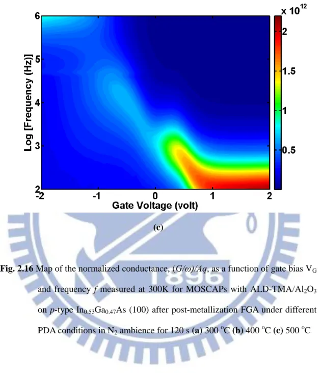
Fig. 2.10 (a), Fig. 2.16 (a) (b) (c) and Fig. 2.11 (b), Fig. 2.17 (a) (b) (c) show
conductance maps of Al2O3/TMA-treated In0.53Ga0.47As MOSCAPs with FGA under
different PDA conditions, on both p- and n-type (100)-oriented In0.53Ga0.47As,
19
conductance (G/ω)/Aq as a function of ac frequency f and the gate voltage VG. For the
p-type MOSCAPs, all plots show that a distinct signal exists at the positive gate voltage and lower frequency. The color variation in this region is getting dramatic as the temperature of PDA is above 400 oC. We speculate that the amount of interface states considerably increases as the temperature of PDA is getting higher. For the plot of PDA 500 oC for 120 s, there is an additional signal existing at gate voltage between -2 and -1 volt and higher frequency; furthermore, we also observe that the conductance is constant at gate voltage between 1 and 2 volts, indicating minority carrier response. For the n-type MOSCAPs, there is a conspicuous variation in color appearing at the negative gate voltage in all graphs, which implies that energy loss is dramatically rising. Similarly, the G-V response to this energy loss is made by interface states owing to its gate-voltage dependent and frequency-dependent conductance. Additionally, the signal existing between VG= 1 and VG= 2 volts and
higher frequency becomes distinct as the temperature of PDA increases.
Fig. 2.18 (a) (b), and (c) show X-ray photoelectron spectroscopy of ALD-TMA
(10 cycles)/Al2O3 (10 cycles) on (100)-oriented In0.53Ga0.47As with post-metallization
FGA under various PDA conditions. XPS scans of Ga 2p3/2, In 3d5/2, and As 2p3/2 core
levels are taken. From Fig. 2.18 (a) and (b), we observe that there is no significant change in Ga 2p3/2 and In 3d5/2 spectra. The As 2p3/2 spectra, shown in Fig. 2.18 (c),
demonstrates that As-As bonds are present in these PDA conditions. It is noted that the concentration of As-As states dramatically increases under PDA 500 oC. We also find that a lower binding energy peak, which is labeled As- in the spectra, is detected on the samples with PDA 500 oC for 120s. This may be an indication of breaking of As-As states at the surface, creating an arsenic dangling bond. In addition, the ratio of As2O3 to As2O5 at PDA 500 oC is the lowest. Table 2.3 shows the ratio of the fitted
20 for the In0.53Ga0.47As (100).
The results suggest that the considerable existence of As-As states or As- states and As2O5 at the interface should be avoided, causing the degradation of electrical
characteristics. The reason for the degradation of C-V characteristics with PDA 500
o
C for 120 s may be the precipitation of arsenide and lower ratio of As2O3 to As2O5
(As2O3 to As2O5). High temperature annealing results in the excess arsenic atoms
produced either the decomposition of In0.53Ga0.47As itself or the chemical
transformation of the oxide species through reactions with the In0.53Ga0.47As channel
layer. The elemental arsenide overlayer acted as a metallic contamination source nearby the interface between oxide and substrate increases the surface recombination velocity, deteriorating insulator properties [36]. In addition, the possibility that a little amount of arsenic oxides diffused into the Al2O3 during post deposition annealing at
temperature above 300 oC cannot be excluded.
2.4 Electrical Characteristics of ALD-TMA/In
0.53Ga
0.47As
(111)A and Interfacial Chemistry
There have been few studies regarding the MIS properties on the (111) surface of III-V semiconductors. Some previous research showed that the electrical characteristics of (111)A-oriented In0.53Ga0.47As and (111)A-oriented GaAs MIS
capacitors with Al2O3 dielectrics deposited by ALD were comparable to or even better
than those on the (100)-oriented In0.53Ga0.47As and (100)-oriented GaAs MIS
capacitors [37-39]. Besides, since the former approach has succeeded in forming uniform and dislocation-free InGaAs layers on Si (111), the characteristics of
21
MISFET on the (111)-oriented InGaAs are of great interest [40].
Fig. 2.19 (a) (b) (c) (d) show multifrequency C-V curves of MOSCAPs with a
Al2O3 film on p-type TMA treated (111)A-oriented In0.53Ga0.47As after
post-metallization FGA under different PDA conditions, measured at 300K. The frequency dispersion at VG= -2 slightly improves at PDA of 300 oC and 400 oC but
degrades at PDA of 500 oC, shown in Table 2.2. At positive gate bias, the capacitance remarkably increases at lower frequency compared to our previous C-V curves of
p-type In0.53Ga0.47As MOSCAPs with (100) orientation, shown in Fig. 2.8 (a) and Fig.
2.14 (a) (b) (c). We suppose that the inversion response appears at more positive gate
voltages and lower frequency due to the constant capacitance.
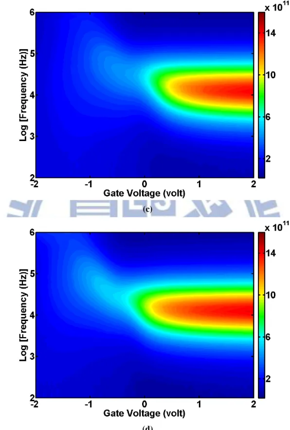
Fig. 2.20 (a) (b) (c) (d) show conductance maps of Al2O3/TMA-treated
In0.53Ga0.47As MOSCAPs with FGA under different PDA conditions, on p-type
(111)A-oriented In0.53Ga0.47As at temperature 300K. These maps show the magnitude
of normalized conductance (G/ω)/Aq as a function of ac frequency f and the gate voltage VG. Under various PDA conditions with FGA, we could easily observe the
minority carrier response at more positive gate bias in all graphs, and the as-deposited one with FGA demonstrates the strongest minority carrier response. The response of interface states also exists at gate voltage between -1 and 0 volt.
Fig. 2.21 (a) (b), and (c) show X-ray photoelectron spectroscopy of ALD-TMA
(10 cycles)/Al2O3 (10 cycles) on (111)A-oriented In0.53Ga0.47As with
post-metallization FGA under various PDA conditions. XPS scans of Ga 2p3/2, In
3d5/2, and As 2p3/2 core levels are taken. From Fig. 2.21 (a) and (b), we observe that
there is no significant change in Ga 2p3/2 and In 3d5/2 spectra. The As 2p3/2 spectra,
shown in Fig. 2.21 (c), demonstrates that the As- component dramatically increases under PDA 500 oC for 120 s. Furthermore, the ratio of As2O3 to As2O5 slightly
22
shows the ratio of the fitted area of the As-As and As- components and As2O3 to
As2O5 from the As 2p3/2 spectra for the In0.53Ga0.47As (111)A.
2.5 Conductance Method
Methods of quantifying Dit, the trap level energy position and the degree of
Fermi level (un)pinning are important in the development of high quality interface between high-κ dielectric and III-V materials [41-43]. It is often impractical to fabricate MOSFET for III-V devices because the transistor fabrication process may introduce other issues. Therefore, MOSCAP structures are commonly used to study the dielectric/substrate interface, dating back to 1960s. The conductance method including the effects of the energy distribution of interface states in the bandgap and surface potential fluctuation (SPF), which has been established by Nicollian and Geotzberger, is a powerful and sensitive tool to determine Dit. Fig 2.22 (a) shows that
a n-type MOSCAP applies to a small amplitude (~25 mV) ac signal with frequency f (typically between 1 MHz and 100Hz) superimposing on a dc gate bias, Vg. Also
shown are the conduction and valence band DOS, Ddos, an arbitrary interface states
density distribution, the Fermi level EF and the intrinsic level EI. Fig. 2.22 (a)
assumes that the band diagram of this MOSCAP is in depletion region. The gate voltage, inducing a space charge and band bending,ψs ,determines the Fermi level
position at the interface. A periodic change in ψs is caused by the ac small signal and
the Fermi level at the interface oscillates around the energy level position determined by the dc gate bias. Only traps with energy levels that are near the Fermi level are able to change their occupancy. An equivalent circuit model for a MOSCAP with interface states in depletion region, including the gate oxide capacitance, Cox, the
23
semiconductor capacitance, Cdos(ω,ψs), interface trap capacitance, Cit(ω,ψs),
equivalent parallel conductance, Gp(ω,ψs) and a series resistance, Rs, is shown in Fig.
2.22 (b). The circuit model shown in Fig. 2.22 (b) assumes that the minority carrier
response is negligible. Fig. 2.22 (c) shows the equivalent circuit of impedance analyzer with the measured capacitance, Cm, and conductance, Gm. The frequency
dependence is related to the characteristic trap response time,
2 ,
where ω is the angular frequency, f
2 (f=measurement frequency)
The interface trap capacitance is related to the interface states density by
it it q D
C 2 ,
where q is the elemental charge
The trap response time for electron or hole is given by Shockley-Read-Hall statistics of capture and emission rate:
T k E E N T k E E N B v t v h th h B t C c e th e exp exp 1 , 1 , , (2.3)where Et is the trap energy in the band gap, σ is the capture cross section, νth is the
average thermal velocity of majority carriers, N is the effective density of states of the majority carrier band, kB is the Boltzmann constant, and T is the temperature.
The conductance method is based on analyzing the loss that is caused by the change in the trap level charge state. Gp/ω is given in terms of the measured
capacitance, Cm, the oxide capacitance, Cox, and the measured conductance, Gm, by
24 2 2 2 2 ) ( ox m m ox m p C C G C G G (2.4)
For continuum trap level, the time constant dispersion must be taken into
account and the normalized conductance is shown as follows:
2
1 ln 2 it it it p qD G (2.5)Maximum loss occurs when interface traps are in resonance with the applied ac signal. For Eq. (2.3) we find
max 5 . 2 p it G Aq D as it 2 (2.6)
where A is the device area. Et can be determined from the frequency at (Gp/ω)max and
applying Eq. (2.5). Fig. 2.23 (a) (b) show trap level position calculated from Eq. (2.3) using the values for the average thermal velocity and the band DOS for In0.53Ga0.47As
and a capture cross section σ = 1×10-17 cm2. The characteristics trap frequency as a function of temperature determines the part of interface traps in the band gap observable in the MOS admittance characteristic. Fig. 2.23 (a) shows the characteristics trap frequency as the function of trap energy in the band gap under different temperature (300K, 250K, 200K, 150K, 100K, and 77K). Due to typical measurement frequency between 100 Hz and 1M Hz, it’s impossible to extract the interface state density over the whole band gap at room temperature. However, by varying the temperature, the complete Dit profiles can be done. For the band gap
around 0.74 eV of In0.53Ga0.47As, traps near midgap could be observed at room
temperatures. The traps closer to the band edges could be probed by measuring the impedance at lower temperature because of increase of the trap response time. Fig.
2.23 (b) shows the traps energy as a function of temperature at frequency 100 Hz
25
windows at given temperature and the limited range of typical measurement frequency.
2.5.1 Comparison between FGA and PMA
Fig. 2.24 (a) (b) and Fig. 2.25 (a) (b) show conductance maps of
Al2O3/TMA-treated In0.53Ga0.47As MOSCAPs with FGA or with PMA, on both p- and
n-type (100)-oriented In0.53Ga0.47As, respectively, at temperature 300K. These maps
show the magnitude of normalized parallel conductance (Gp/ω)/Aq as a function of ac
frequency f and the gate voltage VG. The Dit is estimated by multiplying the peak value,
[(Gp/ω)/Aq]max, with a factor of 2.5[see Eq. 2.6]. In Fig. 2.24 (b), there is a
remarkable response appearing at VG= -2 volts and frequency between 1 kHz and 100
Hz. We speculate that this response might be slow traps or border traps [section 2.3.2]. The samples with FGA, shown in Fig. 2.24 (a), don’t show the response at the same region, which indicates H2 annealing is able to passivate these slow traps and reduces
the frequency dispersion in accumulation. For n-type MOSCAPs, we also observe that the slow traps are effectively passivated by hydrogen annealing and lower interface states exist in the samples with FGA [Fig. 2.25(a)].
Fig. 2.26 (a) (b) and Fig. 2.27 (a) (b) show the parallel conductance curves of
Al2O3/TMA-treated In0.53Ga0.47As MOSCAPs with FGA or with PMA, on both p- and
n-type (100)-oriented In0.53Ga0.47As, respectively, at temperature 300K by using Eq.
2.4. The Gp/ω-f curves from VG= -1 to 1 volt for p-type and VG= 0.5 to -1.5 volts for
n-type are demonstrated here, and Dit can be obtained by multiplying peak value with
a factor of 2.5. It is clearly known that MOSCAPs with FGA have lower interface states than MOSCAPs with PMA. According to Eq. 2.3, the frequency corresponding


![HPSH [ 氧化數平衡反應式係數 ]](data:image/gif;base64,R0lGODlhAQABAIAAAP///wAAACH5BAEAAAAALAAAAAABAAEAAAICRAEAOw==)